


Recently, Hangzhou Garen Semiconductor Co., Ltd. (hereinafter referred to as “Garen Semiconductor”) has followed a China-characteristic development path. Based on its self-developed casting-based single crystal growth technology and MOCVD epitaxial process, the company has delivered the world’s first 6-inch (100)-oriented gallium oxide homoepitaxial wafer to leading customers and has achieved stable mass production and shipment.
Technical Strength Leading the Field
In the crystal growth stage, Garen Semiconductor relies on its globally unique casting growth method to stably produce ultra-thick gallium oxide single crystals. By combining its proprietary ultra-thin substrate processing technology, the company has increased substrate output by 3–4 times compared with conventional approaches. In addition, the casting growth method significantly reduces the consumption of the precious metal iridium, lowering per-wafer substrate cost by more than 80%, and substantially reducing material costs for downstream device manufacturers.
In the epitaxy stage, the technical team optimized key process parameters specifically for the (100) orientation and developed a proprietary MOCVD epitaxial process. As a result, the company has become the world’s first and only commercial supplier of 6-inch gallium oxide homoepitaxial wafers. The epitaxial layers of its 6-inch Ga₂O₃ homoepitaxial wafers exceed 10 μm in thickness, with film thickness variation below 1%, demonstrating excellent uniformity. These characteristics make the wafers highly suitable for high-performance device fabrication and significantly improve yield assurance for device manufacturers.
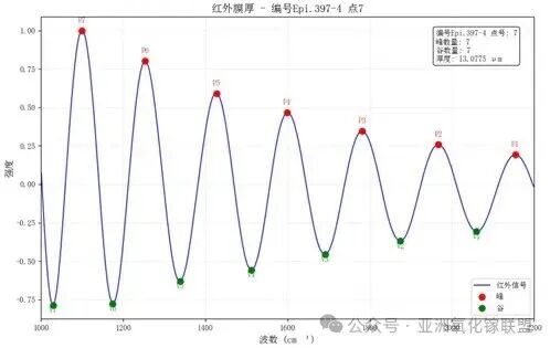
Figure 1. 6-inch Ga₂O₃ homoepitaxial wafer: Fourier transform infrared (FTIR) reflectance spectrum.
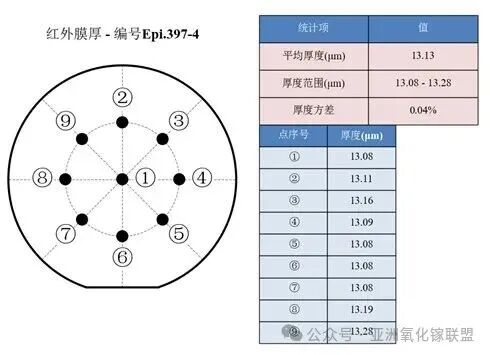
Figure 2. 6-inch Ga₂O₃ homoepitaxial wafer: Mapping of film thickness measurement points and corresponding results.
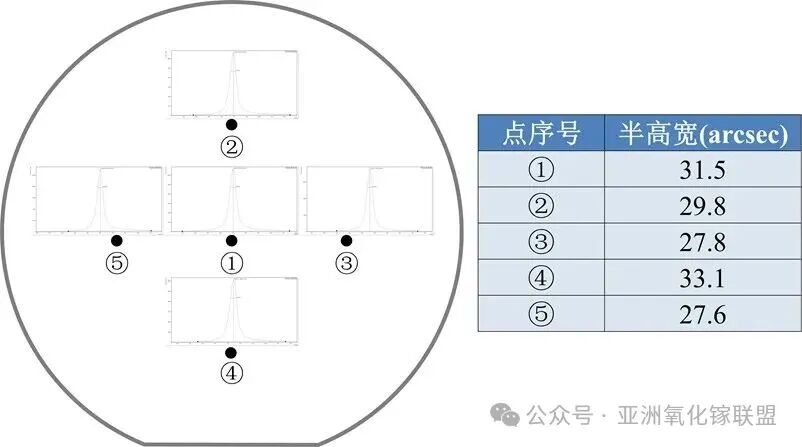
Figure 3. 6-inch Ga₂O₃ homoepitaxial wafer: High-resolution X-ray diffraction (HRXRD) rocking curve and corresponding measurement results at different locations.
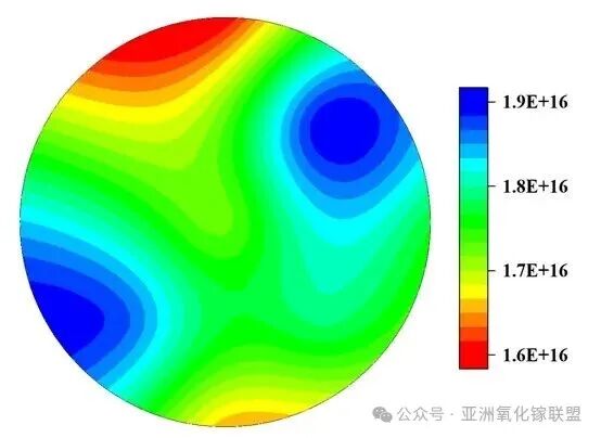
Figure 4. 6-inch Ga₂O₃ homoepitaxial wafer: Contour map of carrier concentration distribution.
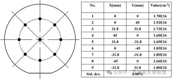
Figure 5. 6-inch Ga₂O₃ homoepitaxial wafer: C–V measurement point distribution and corresponding results.
Stable Capacity Supply
Previously, homoepitaxial gallium oxide wafers faced global bottlenecks such as small wafer size, limited production capacity, and poor uniformity, making it difficult to meet industrial-scale demands. In this latest development, Garen Semiconductor has not only achieved the world’s first delivery of a 6-inch Ga₂O₃ homoepitaxial wafer, but has also established a fully integrated and stable mass-production capability covering the entire “single crystal growth–substrate–epitaxy” workflow.
The company has built the world’s first 6-inch/8-inch Ga₂O₃ homoepitaxial production line, with consistent and controllable batch-to-batch quality. Multiple overseas companies and research institutions have already placed orders, and several partners are engaging in long-term stable procurement.
From equipment design and crystal growth to epitaxial processing, Garen Semiconductor adheres to full-chain independent controllability. Through an innovation-driven and distinctive development pathway, the company highlights the “China speed” in Ga₂O₃ industrialization and continuously provides strong momentum for building a complete domestic gallium oxide supply chain.
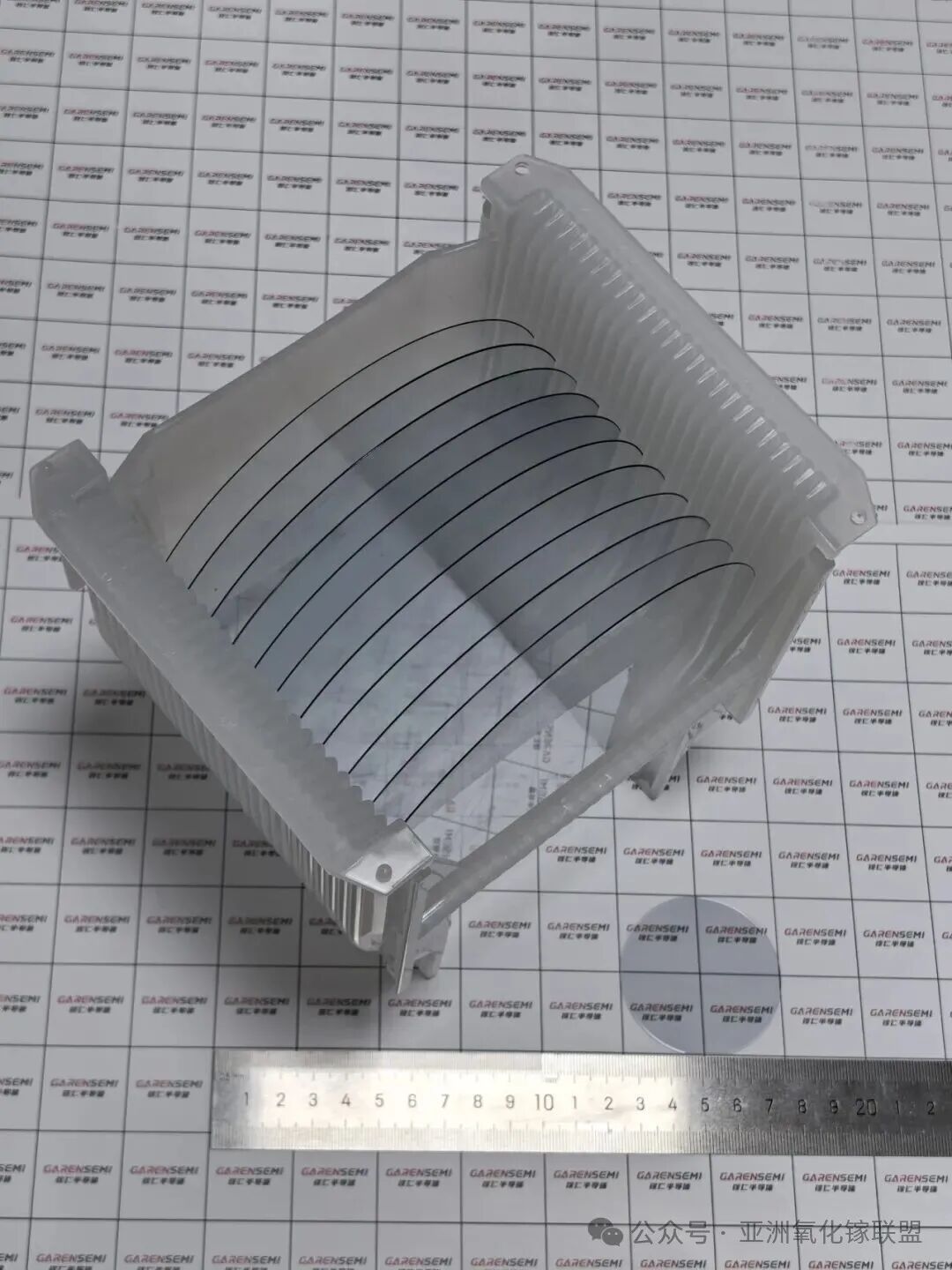
Figure 6. Mass Production and Shipment of 6-inch Ga₂O₃ Homoepitaxial Wafers Achieved
(The 2-inch Ga₂O₃ homoepitaxial wafer from Garen Semiconductor shown in the lower-right corner is provided for size comparison.)
About GAREN SEMI
Hangzhou Garen Semiconductor Co., Ltd. is a world-leading provider of Gallium Oxide materials and equipment solutions, focusing on R&D and industrialization in the ultra-wide bandgap semiconductor field. The company’s core products include 2–8-inch Gallium Oxide single crystals and substrates (with 8-inch being the world’s first), Gallium Oxide Vertical Bridgman (VB) crystal growth equipment, Gallium Oxide epitaxial wafers, etc. It is committed to building a full-chain product system of “equipment–crystal–substrate–epitaxy” to provide systematic solutions for global customers. The company’s achievements in Gallium Oxide have been specially reported by well-known media including People’s Daily, Xinhua News Agency, Science and Technology Daily, Sina Finance, China Blue News, and The Paper.
For more information about Garen Semiconductor and its products, please visit our official website: http://garen.cc/
Or contact us via the following ways:
Mr. Jiang: 15918719807
E-mail: jiangjiwei@garen.cc
Mr. Xia: 19011278792
E-mail: xianing@garen.cc
Instruction
Official Account

Cooperation
Top
