


In the previous installment, we introduced the fundamental principles of several mainstream melt-growth technologies for gallium oxide. Among them, the Czochralski (CZ) method, Edge-Defined Film-Fed Growth (EFG) method, and Vertical Bridgman (VB) method have all been successfully employed for the fabrication of large-size β-Ga₂O₃ single-crystal substrates.
From a technological perspective, each approach has its own strengths. The CZ method is a mature and well-established representative of conventional melt-growth crystal technologies. As an emerging route, the VB method has demonstrated considerable potential in large-size crystal growth and crystallographic orientation flexibility. The EFG method, meanwhile, has become one of the fastest-advancing routes toward the commercialization of gallium oxide substrates, owing to its advantages in shape controllability, relatively high production efficiency, and extensive device-validation experience.
This article focuses on “the leading pathway toward gallium oxide substrate commercialization.” By reviewing the current development status of the CZ, EFG, and VB melt-growth routes, we aim to analyze the practical advantages and industrial foundation that have enabled EFG technology to play a leading role in the commercialization of gallium oxide substrates.
Gallium oxide has attracted significant attention in the power semiconductor community, largely because bulk single crystals can be produced using melt-growth techniques. This characteristic provides potential advantages over materials such as GaN and SiC in terms of substrate cost and scalability.
However, transitioning from material research to industrial applications requires far more than simply demonstrating the ability to grow crystals.
Commercial-grade gallium oxide substrates must satisfy multiple requirements simultaneously. Crystal dimensions must be sufficiently large, while wafer-level uniformity must remain stable. Defects, twins, and cracking must be well controlled. Electrical properties of conductive or semi-insulating substrates must be reliably tunable. In addition, downstream processes—including slicing, grinding, polishing, and epitaxial growth—must be seamlessly integrated into the manufacturing flow.
As a result, substrate commercialization is not merely a competition in crystal growth capability. Rather, it is a comprehensive competition involving crystal size, material quality, cost, yield, and compatibility with downstream device manufacturing.
Within this context, the CZ, EFG, and VB methods represent different engineering philosophies. The CZ method emphasizes a mature crystal-ingot growth foundation, the VB method focuses on the potential of large-size directional solidification, while the EFG method is inherently more aligned with substrate manufacturing requirements due to its shape controllability and higher production efficiency. For this reason, EFG has emerged as one of the most prominent and widely recognized routes for gallium oxide substrate commercialization.
The CZ method is one of the most mature and widely adopted technologies for melt-grown single crystals. In this process, a seed crystal is brought into contact with the melt and then slowly pulled upward while rotating, allowing the crystal to grow progressively from the molten material. The development of the silicon single-crystal industry is largely built upon decades of process optimization based on CZ technology.
For β-Ga₂O₃, the CZ method also offers significant advantages. It can produce nearly cylindrical crystal ingots, facilitating subsequent processing into circular wafers. It is also well suited for fundamental research involving substrate orientation engineering, doping control, and high-quality crystal growth.
However, when applied to large-scale commercial production of gallium oxide substrates, the CZ method faces several notable engineering challenges.
One of the primary challenges lies in balancing high-temperature decomposition and crucible degradation. At elevated temperatures, β-Ga₂O₃ tends to thermally decompose, generating volatile species such as Ga and Ga₂O. To maintain melt stability and suppress decomposition, a certain oxygen partial pressure is typically required during growth. However, elevated oxygen partial pressure simultaneously accelerates oxidation and evaporation of the iridium (Ir) crucible, increasing precious-metal consumption and ultimately driving up substrate costs.
As crystal size continues to increase, issues associated with Ir crucible cost, melt stability, and prolonged high-temperature exposure become increasingly severe. Larger crystals generally require larger melt volumes and crucibles, as well as longer growth and thermal holding durations. Consequently, stricter control over oxygen partial pressure, suppression of Ga₂O₃ decomposition, and extension of crucible lifetime become essential. As shown in Figure 1, the amount of liquid Ga present in the Ga₂O₃ melt during crystal scaling from 1 inch to 4 inches is closely related to oxygen concentration.
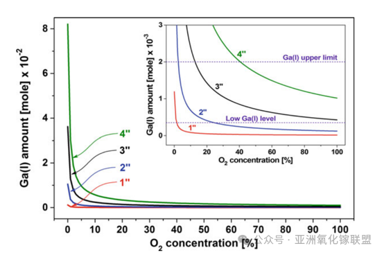
Figure 1. Relationship between the amount of liquid Ga in the Ga₂O₃ melt and O₂ concentration during 1–4 inch crystal growth [1].
In addition, for conductive substrates used in power devices, higher carrier concentrations help reduce substrate resistance. However, excessive doping levels introduce new crystal-growth challenges. As the free-electron concentration increases, free-carrier absorption in the near-infrared region becomes stronger. Consequently, the latent heat of crystallization, which is normally dissipated through radiative heat transfer, can no longer be released efficiently. This may alter the temperature distribution and interface morphology near the solid–liquid interface [2].
When interface stability deteriorates, crystal diameter control and shape control become increasingly difficult. In severe cases, abnormal growth morphologies such as spiral growth may occur, as illustrated in Figure 2.
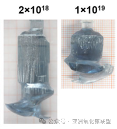
Figure 2. Spiral crystal growth under high carrier concentration conditions [3].
Therefore, despite its mature process foundation and strong crystal-quality control capability, the CZ method still faces challenges related to crucible consumption, atmosphere control, thermal-field stability, and highly doped crystal growth when targeting large-size, low-cost, and stable mass production of gallium oxide substrates.
In recent years, the VB method has attracted growing attention in the field of gallium oxide substrate fabrication.
Compared with the other two growth methods, one notable advantage of the VB approach is its ability to utilize Pt/Rh alloy crucibles and operate under ambient air or elevated oxygen partial pressure environments. Higher oxygen partial pressures help suppress the thermal decomposition of gallium oxide at elevated temperatures, providing advantages in stoichiometry control and stable crystal growth.
Furthermore, the VB method can produce nearly cylindrical crystals, which can subsequently be sliced along different crystallographic orientations. For β-Ga₂O₃, a material with pronounced anisotropic properties, this orientation flexibility is highly attractive.
According to published reports, the VB method has already demonstrated the growth of β-Ga₂O₃ single crystals as large as 12 inches in diameter [4,5], highlighting its considerable potential for large-size crystal fabrication and quality improvement.
Nevertheless, as an emerging technology route, several aspects of the VB method still require further validation.
On one hand, Pt/Rh alloy crucibles may introduce metallic impurities such as Rh into the crystal. Studies have reported Rh concentrations ranging from several ppm to several tens of ppm in VB-grown crystals [6]. For power-device applications, the potential impact of such impurities on epitaxial quality, leakage current, breakdown stability, and long-term reliability remains to be systematically evaluated.
On the other hand, compared with EFG substrates—which have already been widely adopted for homoepitaxial growth and device development—VB substrates have accumulated relatively limited downstream device-validation data. Their batch-to-batch consistency, epitaxial compatibility, and long-term reliability will require further confirmation through additional epitaxial growth and device-performance studies.
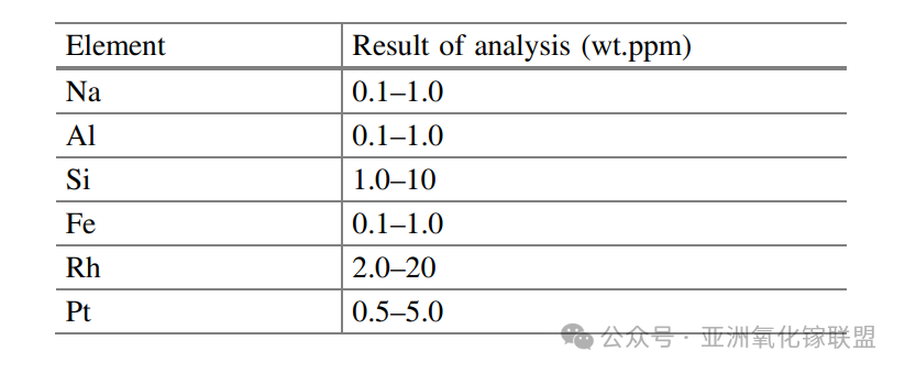
Table 1. Analysis of impurity concentrations in VB-grown crystals [6].
From a commercialization perspective, whether a substrate growth technology can be the first to achieve widespread adoption depends not only on whether a particular performance metric is superior, but also on whether it can continuously provide a stable, verifiable, and scalable material platform.
The EFG method was conceived with substrate manufacturing requirements in mind from the outset, making it naturally aligned with the logic of commercial supply. Compared with large-melt-volume approaches such as the CZ method, EFG can operate under lower oxygen-content growth environments, reducing iridium (Ir) crucible consumption, degradation, and depreciation costs, thereby improving substrate cost efficiency. At the same time, its flexibility in shape and size design facilitates the establishment of standardized wafer manufacturing processes.
For β-Ga₂O₃, which is still in the early stages of industrial adoption, the ability to rapidly provide substrates with stable specifications, consistent quality, and reliable deliverability is often more valuable than simply pursuing larger crystal dimensions. This is one of the key reasons why EFG has become one of the earliest growth technologies to gain recognition in the commercial gallium oxide substrate market.
Precisely because of its close alignment with substrate manufacturing requirements, EFG entered the industrial cycle of “material supply – epitaxial growth – device validation” at an earlier stage. For any emerging semiconductor material, process maturity can only be achieved through continuous downstream use, verification, and feedback. The early commercial availability of EFG substrates enabled epitaxy and device development teams to carry out structural design, process optimization, and reliability evaluation on a relatively stable material platform.
Today, many homoepitaxial growth and device studies based on gallium oxide are conducted using EFG substrates, including research on Schottky barrier diodes, field-effect transistors, and solar-blind ultraviolet photodetectors. As these studies continue to accumulate, EFG substrates have gradually established a relatively complete validation ecosystem spanning the material, epitaxy, and device levels.
This validation foundation itself represents a significant advantage during the early stages of commercialization. It demonstrates not only that the material can be supplied, but also that it can be consistently integrated into downstream manufacturing processes.
At present, EFG-grown gallium oxide substrates have progressed from 2-inch and 4-inch formats toward 6-inch and even 8-inch diameters. However, wafer scaling is not merely a matter of increasing physical dimensions; it is a comprehensive challenge involving crystal quality control, within-wafer uniformity, and epitaxial compatibility. For industrial adoption, the key question is whether high-quality substrates can continue to be produced and delivered with stable, measurable, and reproducible performance at larger wafer sizes. The answer to this question will largely determine whether the EFG route can move toward large-scale commercialization.
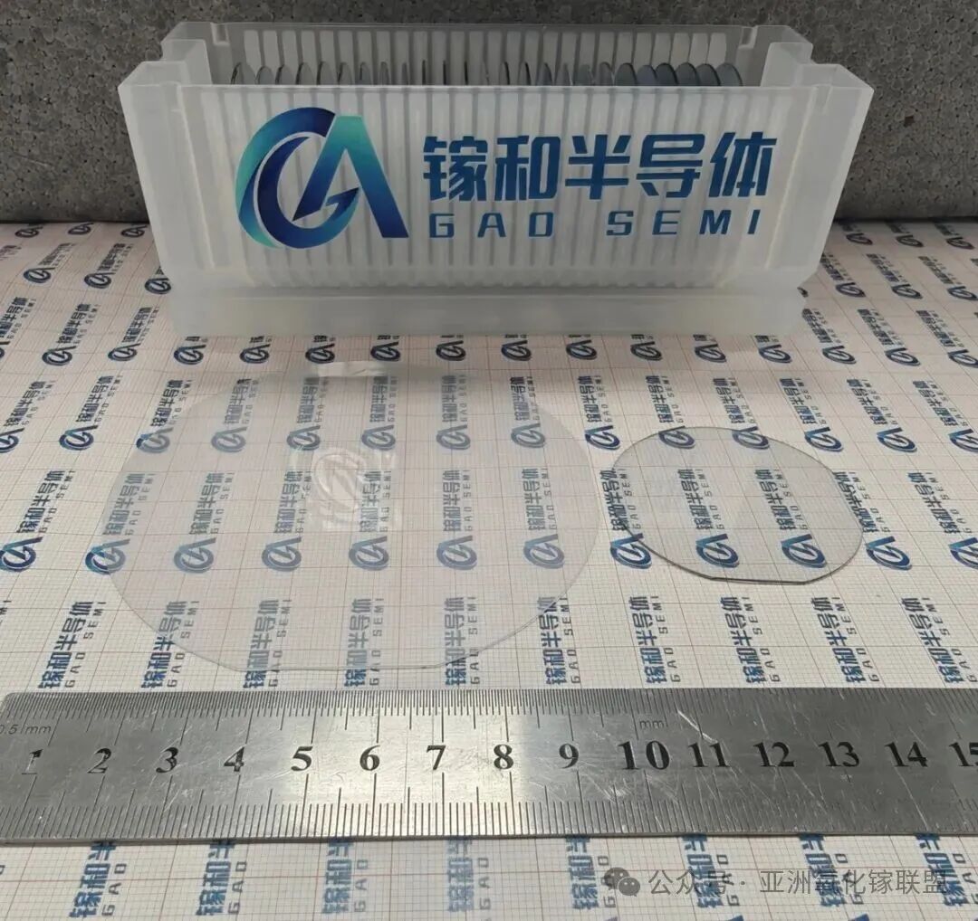
Figure 3. High-quality 2–4 inch Ga₂O₃ single-crystal substrates.
Currently, G&H Semiconductor has achieved stable production of high-quality 2–4 inch Ga₂O₃ single-crystal substrates using the EFG method and has established a continuous and reliable substrate supply capability. As shown in Figure 3, the fabricated substrates exhibit intact surface appearance and consistent dimensions.
Figure 4 presents a cross-sectional polarized optical microscopy image of a 2-inch β-Ga₂O₃ substrate with a (001) principal surface. No obvious twin defects are observed within the main body of the substrate, indicating excellent crystal quality.
Further characterization using a nine-point X-ray diffraction (XRD) rocking curve measurement shows that the full width at half maximum (FWHM) values are all below 50 arcsec, demonstrating high crystallographic quality and excellent within-wafer uniformity.
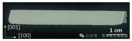
Figure 4. Cross-sectional polarized optical microscopy image of a 2-inch β-Ga₂O₃ substrate with a (001) principal surface.
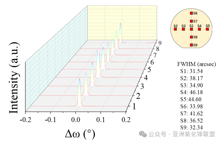
Figure 5. Results of the nine-point XRD rocking curve measurements.
In addition, atomic force microscopy (AFM) characterization reveals that the root-mean-square (RMS) surface roughness at all nine measurement locations is below 0.2 nm, as shown in Figure 6, indicating an atomically smooth surface morphology.
The combination of high crystal quality and excellent surface condition provides a reliable foundation for subsequent high-quality homoepitaxial growth and offers important support for the continued development of Ga₂O₃-based power electronic devices and ultraviolet optoelectronic devices.
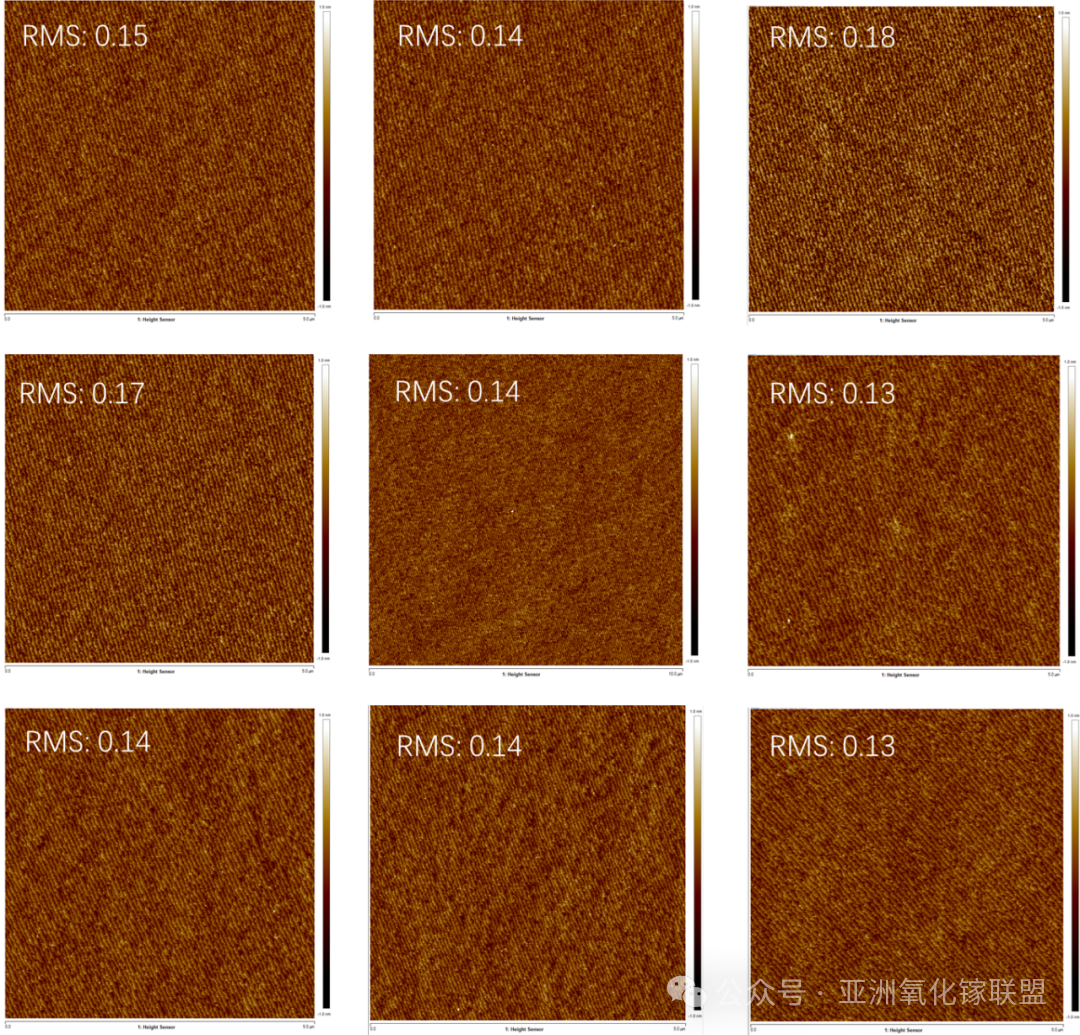
Figure 6. Results of the nine-point AFM measurements.
Overall, the CZ method remains highly valuable for high-quality crystal growth and fundamental research due to its mature technological foundation. However, challenges associated with iridium crucible consumption and growth stability under high doping conditions continue to limit its potential for low-cost, large-scale production of gallium oxide substrates.
The VB method, as a rapidly developing emerging technology, has demonstrated considerable promise for large-size crystal growth. Nevertheless, further validation is still required regarding impurity control, epitaxial compatibility, and long-term device reliability.
In contrast, the EFG method has achieved an earlier alignment with the practical requirements of commercial substrate manufacturing while simultaneously accumulating a substantial foundation in material supply, epitaxial growth, and device validation. As a result, it has become one of the leading pathways driving the commercialization of gallium oxide substrates today.
More importantly, EFG was the first route to bring gallium oxide into a complete industrial cycle encompassing substrate supply, epitaxial growth, and device validation. As this ecosystem continues to mature, it will provide an increasingly stable material platform for future process optimization, performance enhancement, and application expansion.
As large-diameter substrate manufacturing capabilities continue to improve, competition within the gallium oxide industry will gradually shift from the question of whether single crystals can be grown to whether high-quality substrates suitable for device fabrication can be supplied consistently, economically, and at scale.
In this transition, the EFG method is expected to remain one of the key technologies driving the commercialization of gallium oxide substrates.
References:
[1] Galazka Z, Uecker R, Klimm D, Irmscher K, Naumann M, Pietsch M, Kwasniewski A, Bertram R, Ganschow S, Bickermann M, ECS J. Solid State Sci. Technol. 6, Q3007 (2017)
[2] Galazka Z. Growth of bulk β-Ga₂O₃ single crystals by the Czochralski method. Journal of Applied Physics, 2022, 131: 031103.
[3] Galazka Z, Irmscher K, Uecker R, Bertram R, Pietsch M, Kwasniewski A, Naumann M, Schulz T, Schewski R, Klimm D, Bickermann M, J. Cryst. Growth 404, 184 (2014)
[4]https://www.novelcrystal.co.jp/eng/ga2o3-substrate/
[5]https://fujia-hiom.com/fjdt/info/2026/95861.html
[6] Higashiwaki M, Fujita S, eds. Gallium Oxide: Materials Properties, Crystal Growth, and Devices. Vol. 293. Springer Nature, 2020.
Instruction
Official Account

Cooperation
Top
