


The new materials industry is the foundational pillar of high-tech development. Recently released development orientations for the “15th Five-Year Plan” new materials industry across Jiangsu’s 13 prefecture-level cities outline a clear evolutionary blueprint: advanced electronic information materials, represented by cutting-edge semiconductors, have become a frequently mentioned theme and a core growth engine across the province.
North–South Synergy: Cluster Effects in Semiconductor Materials
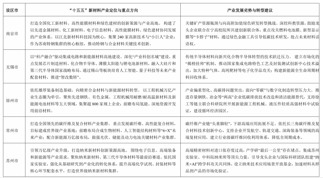
Jiangsu’s semiconductor materials landscape demonstrates a tightly integrated upstream–downstream industrial chain:
Core region of Suzhou–Wuxi–Changzhou (technological leap and frontier breakthroughs):
Wuxi is addressing the technological transition from traditional silicon-based materials to emerging compound semiconductors, with a focus on chip manufacturing materials and compound semiconductors. Suzhou, leveraging national-level laboratories and top-tier research capabilities, is focusing on third-generation semiconductors and packaging materials, building an interdisciplinary innovation ecosystem integrating “nano + AI”.
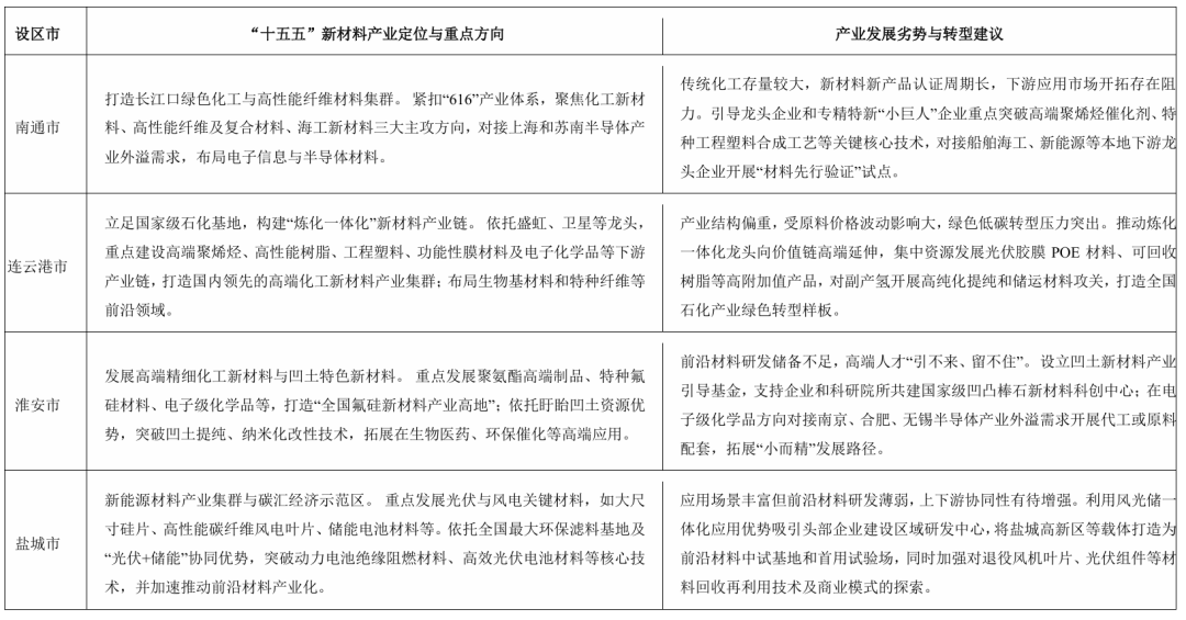
Yangtze River corridor and northern Jiangsu (spillover absorption and supporting capacity):
Nantong is actively aligning with industrial spillover from Shanghai and southern Jiangsu, proactively developing semiconductor materials. Cities such as Huai’an, Yancheng, and Zhenjiang are strengthening their presence in electronic-grade chemicals, large-diameter silicon wafers, specialty gases, and high-purity targets, providing critical raw material supply and pilot-scale support for the province.
Transition Challenges: From “Bottleneck Constraints” to Structural Shift
Despite a strong industrial foundation, structural challenges remain. High-end precision materials still partially rely on imports, and the transition from traditional materials to emerging compound semiconductors faces phased pressure in technological system upgrades and pathway transformation.
To address these issues, the planning framework generally emphasizes two key directions:
Strengthening industry–academia–research integration:
Mechanisms such as “unveiling the leader (guerbanging) challenges” are encouraged to enhance breakthroughs in key technologies and improve the efficiency of technology transfer and commercialization.
Multi-path technology exploration:
While strengthening mature third-generation semiconductor materials such as silicon carbide (SiC) and gallium nitride (GaN), the plan also calls for forward-looking exploration into ultra-wide bandgap materials. In recent years, gallium oxide (Ga₂O₃), which has attracted significant academic and industrial attention, remains at an early engineering stage but is already considered a promising candidate for future high-voltage and high-power applications.
Outlook: Potential Synergy and Validation of Advanced Materials
With the continued expansion of applications in new energy vehicles, energy storage, and high-end equipment manufacturing, demand for ultra-high-voltage and high-power devices is increasing rapidly.
Industrial foundations in cities such as Wuxi and Suzhou—covering high-purity materials, electronic gases, and advanced packaging—provide a natural ecosystem for the development and validation of next-generation semiconductor materials. In the future, supported by well-established pilot platforms and strong regional collaboration mechanisms, these emerging materials may achieve phased validation in specific application scenarios, gradually transitioning from fundamental research to engineering implementation.
Conclusion
Overall, Jiangsu’s “15th Five-Year Plan” for new materials reflects a clear shift from a “silicon-dominated structure” toward a more diversified “compound-semiconductor-enhanced structure.” Compound semiconductor pathways are being continuously expanded, while ultra-wide bandgap materials are naturally entering the frontier exploration stage.
Although industrialization of these advanced materials still requires long-term effort, this tiered and structured planning approach is laying a more resilient foundational support system for both Jiangsu and China’s broader semiconductor industry.
Instruction
Official Account

Cooperation
Top
