


According to a report by China Economic Times, at the 2023 China Optical Valley Jiufengshan Forum and Compound Semiconductor Industry Conference, Academician Hao Yue of the Chinese Academy of Sciences stated that although oxide semiconductors still have some distance to go before large-scale industrial application, their broad application prospects are already clearly visible. Compared with gallium nitride (GaN) and silicon carbide (SiC), oxide semiconductors possess a wider bandgap, theoretically enabling lower conduction losses. However, heat dissipation remains a core bottleneck constraining their industrialization.
Device-level electro-thermal characteristics and reliable physical data constitute an important prerequisite for constructing self-consistent electro-thermal coupling models of ultrawide bandgap (UWBG) semiconductor power devices, conducting steady and transient-state electro-thermal numerical simulations, and performing electro-thermal co-design optimization. Associate Professor Li Yuan from the Faculty of Integrated Circuits at Xidian University has long focused on this critical scientific challenge. Targeting the core issue of device overheating that hinders the maturation of β-Ga₂O₃ power device technology, she has systematically overcome several key characterization and modeling technologies: time-domain thermo-reflectance (TDTR) optical characterization for precise extraction of unknown thermal properties of β-Ga₂O₃ devices, transient thermal imaging (TTI) thermo-reflectance imaging for complex transient electro-thermal characterization of β-Ga₂O₃ devices, and forward physical modeling of β-Ga₂O₃ device electro-thermal coupling integrating material,device and package analysis. On this basis, she has conducted a series of studies on electro-thermal co-design and thermal management system technologies for β-Ga₂O₃ MOS-type trench diodes, MOSFETs, and other devices, establishing a high-precision research framework for electro-thermal coupling modeling and co-optimization design of ultrawide bandgap semiconductor power devices.
Her representative research include:
An Electro-Thermal Co-Designed Ga₂O₃ [100] Trench Power Diode Featuring Ferroelectric Dielectric
Electro-Thermal Co-Design β-Ga₂O₃ MOS-Type Trench Diode Based on Optimized Trench-Sidewall Interface Quality Strategy and Mechanism Study
Implications for FD-OSIQ-Based Electrothermal Co-Design: Degradation of Reverse Performance in β-Ga₂O₃ Ferroelectric Trench Diodes Under Forward-Voltage Stress
Electro-Thermal Improvement in a β-Ga₂O₃ Cage-Integrated Slanted-Fin MOSFET
The Diamond-Plate Double-Side-Cooled β-Ga₂O₃ SBD Prototype with an Ultra-Low RθJC of 0.24 K/W
This series of work breaks through the limitations of traditional single-physics-field design by deeply integrating the coupling mechanisms of electrical and thermal domains. It systematically reveals the physical mechanisms of electro-thermal-field interactions in β-Ga₂O₃ devices under steady- and transient- conditions, providing important theoretical support for device structure optimization, electro-thermal co-design, and improved operational robustness. The established research framework holds significant theoretical value and guiding importance for advancing the engineering application and industrialization of ultrawide bandgap semiconductor power devices.
The following is a report on the third work of this series.
Researchers from the Xidian University and Shandong University and Beijing Microelectronic Technology Institute have published a dissertation titled " Implications for FD-OSIQ-Based Electrothermal Co-Design: Degradation of Reverse Performance in β-Ga2O3 Ferroelectric Trench Diodes Under Forward-Voltage Stress " in IEEE TRANSACTIONS ON ELECTRON DEVICES.
Background
As an ultra-wide bandgap semiconductor, β-Ga₂O₃ possesses an extremely high critical electric field of 8 MV/cm, making it an ideal candidate for high-voltage power devices. The MOS-type trench structure remodels the internal electric field distribution of devices, alleviates leakage current induced by concentrated surface electric field in planar devices, achieves breakdown voltage over 3 kV, and fully unlocks the theoretical performance limit predicted by Baliga’s figure of merit. Nevertheless, two critical bottlenecks restrict the performance improvement of such devices. First, anisotropic dry etching introduces severe damage on trench sidewalls, drastically elevates interface state density and degrades forward conduction current, and devices with [100]-oriented trench sidewalls suffer far more severe performance loss than [010] counterparts. Second, β-Ga₂O₃ exhibits intrinsically low and anisotropic thermal conductivity, with thermal conductivities of 0.27 W/cm·K for [100] trench sidewalls and 0.11 W/cm·K for [010] trench sidewalls, which are much lower than GaN and SiC, leading to severe thermal management challenges.
The optimized sidewall interface quality (OSIQ) strategy incorporating ferroelectric dielectric (FD) utilizes polarized electric field triggered by forward-voltage stress (FVS) to suppress interface states on trench sidewalls. This strategy enables full utilization of superior thermal conductivity along [100]-oriented sidewalls and establishes an electrothermal co-design route to mitigate the intrinsic low thermal conductivity limitation of β-Ga₂O₃. However, previous studies only verified the forward performance enhancement of FD-OSIQ strategy, ignoring the degradation of ferroelectric dielectric, reverse breakdown voltage and leakage current induced by FVS. Besides, leakage degradation under electrical stress has been reported in metal-ferroelectric-metal (MFM) capacitors, yet the long-term reliability and reverse performance degradation mechanisms of FD-OSIQ electrothermal co-design remain unclear. Accordingly, this work fabricates β-Ga₂O₃ MOS-type trench diodes with HfO₂ and ferroelectric HfCeO₂ gate dielectrics, systematically elucidates the complete physical mechanisms of reverse I-V degradation triggered by forward-voltage stress, and provides theoretical guidance for reliable FD-OSIQ electrothermal co-design.
Abstract
The optimized sidewall interface quality (OSIQ) strategy leverages the polarized electric field induced by forward-voltage stress (FVS) in a ferroelectric dielectric (FD) to dramatically relieve the interface state density at trench sidewalls. This enables efficient exploitation of the higher thermal conductivity along the [100]-oriented trench sidewall for β-Ga₂O₃ trench devices, thereby establishing a practical electrothermal co-design pathway that effectively mitigates the intrinsic low thermal conductivity limitation of β-Ga₂O₃. This work further systematically investigates the reverse I-V characteristics of β-Ga₂O₃ MOS-Type trench diodes with ferroelectric HfCeO₂ dielectric, revealing that FVS concurrently degrades the dielectric properties of HfCeO₂ and increases the border trap density. These synergistic degradation mechanisms substantially impair the device’s reverse I-V performance. The findings offer critical theoretical insights and guidance for advancing robust electrothermal co-design in β-Ga₂O₃ trench devices via the FD-OSIQ methodology.
Highlights
This work first reveals an inherent performance trade-off of the FD-OSIQ electrothermal co-design strategy: FVS optimizes trench sidewall interface quality and improves forward conduction, yet simultaneously degrades reverse breakdown voltage and reverse leakage current performance.
Multi-dimensional quantitative characterization of FVS-induced damage on HfCeO₂ ferroelectric dielectric is realized. UV/IR ellipsometry verifies that electrical stress generates oxygen vacancies and lattice distortion, which degrade high/low-frequency dielectric constants and phonon vibration frequencies, clarifying intrinsic dielectric degradation mechanisms from the lattice perspective.
Distinct evolution rules of two types of defects, interface states (Dᵢₜ, Cambria) and border traps (Nᵦₜ, Cambria), are distinguished. It is confirmed that FVS only slightly reduces interface state density but significantly elevates border trap concentration inside dielectrics, identifying border traps as the core defect source responsible for aggravated reverse leakage.
Dominant leakage mechanisms are differentiated between HfO₂ and HfCeO₂ devices: Fowler–Nordheim (FN) tunneling dominates leakage in HSTD devices, while trap-assisted tunneling (TAT) dominates in FSTD devices. FVS intensifies TAT effect in HfCeO₂ devices, and TCAD simulations of electric field and current density fully reproduce the whole degradation process of reverse performance.
A coupled degradation model of reverse performance for ferroelectric trench diodes under forward voltage stress is established, providing comprehensive theoretical support for subsequent reliability improvement and stress degradation suppression of FD-OSIQ strategy.
Conclusion
This work reveals the critical trade-off of the OSIQ strategy in HfCeO₂-based β-Ga₂O₃ MOS-Type trench diodes: improved interface quality is achieved at the cost of degraded reverse capability. It is elucidated that FVS concurrently degrades the dielectric properties of HfCeO₂ and increases the border trap density. Mitigating the impact of such stressinduced degradation will be crucial in the future for realizing robust electrothermal co-designed β-Ga₂O₃ trench devices through the FD-OSIQ approach.
Project Support
This work was supported by NSFC under Grant 62204187.
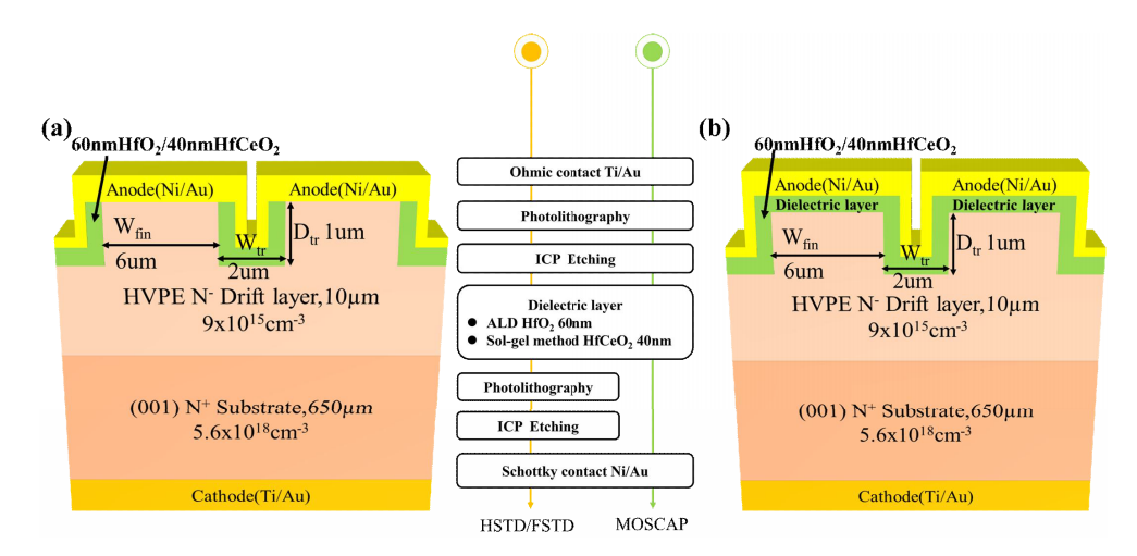
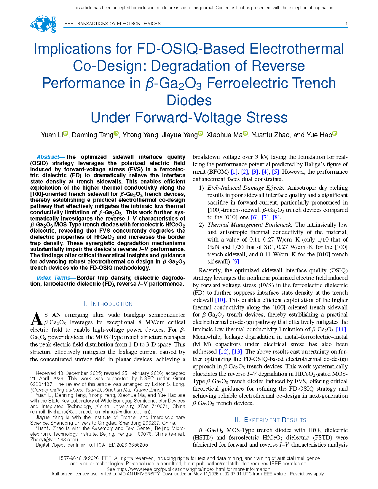
Fig. 1. (a) Cross-sectional schematic of the fabricated β-Ga₂O₃ MOS-Type trench diode with HSTD and FSTD. (b) Cross-sectional schematic of the β-Ga₂O₃ trench MOSCAP with HfO₂ and HfCeO₂ dielectric layer.
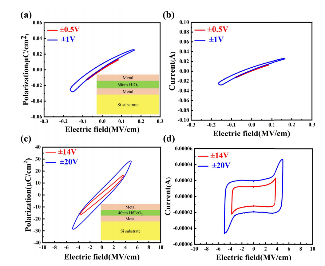
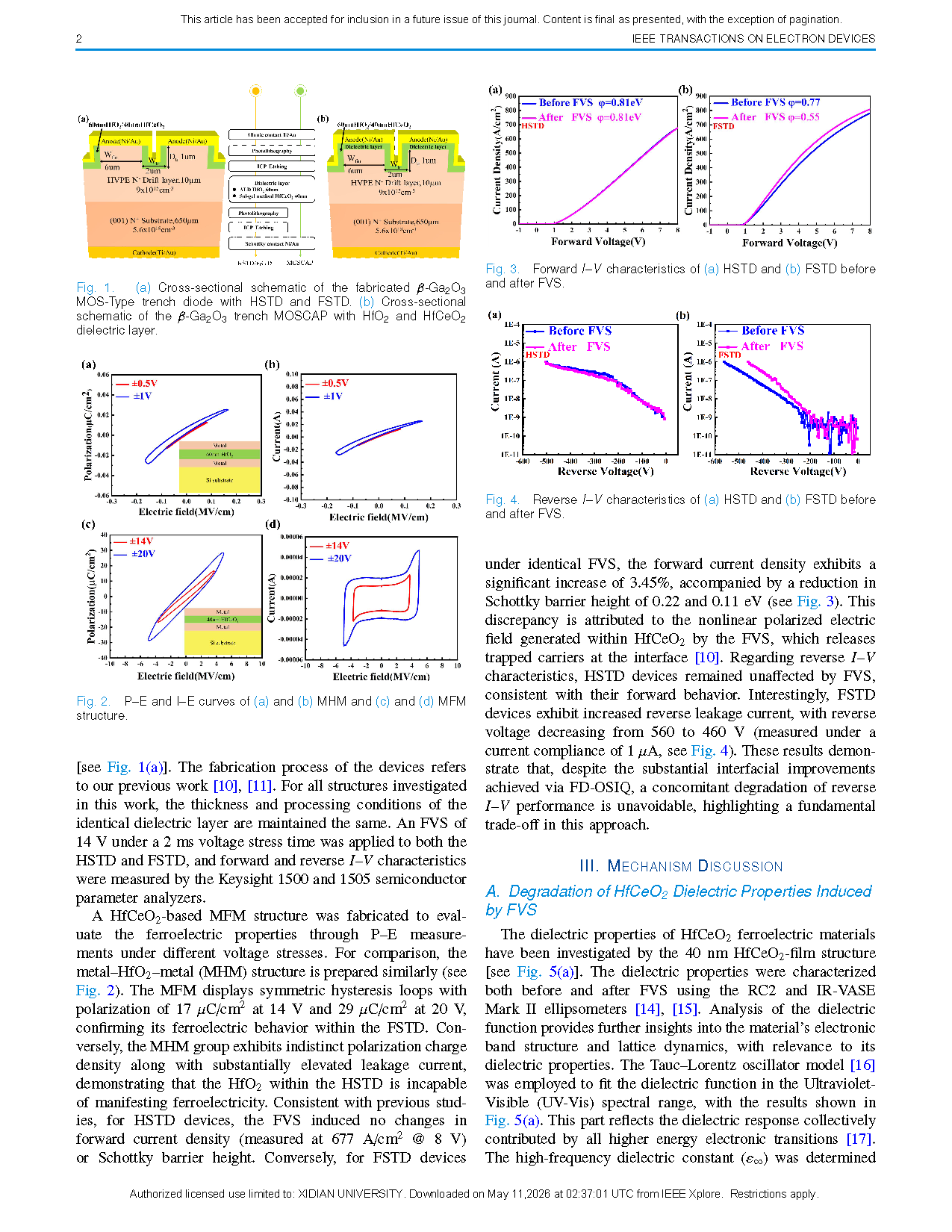
Fig. 2. P–E and I–E curves of (a) and (b) MHM and (c) and (d) MFM structure.
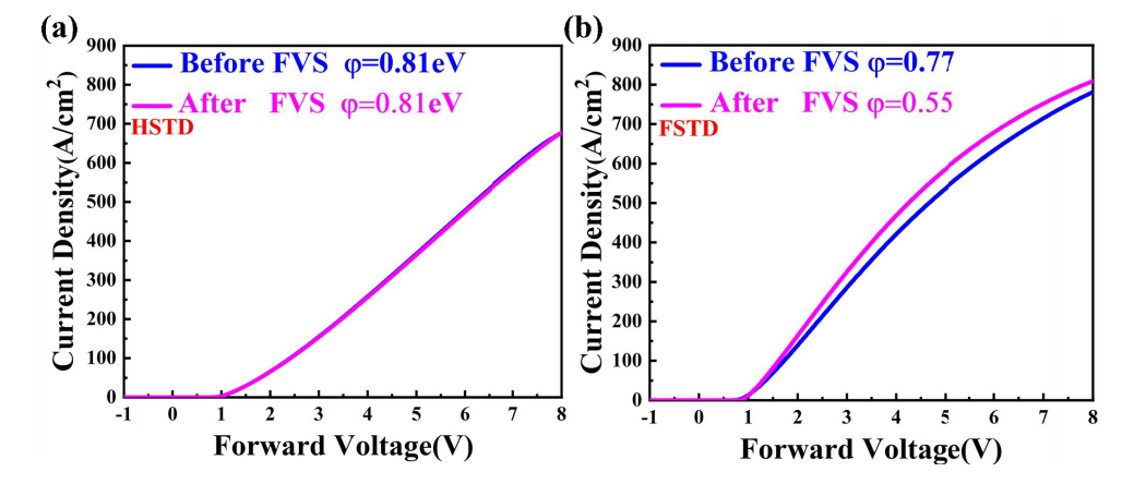
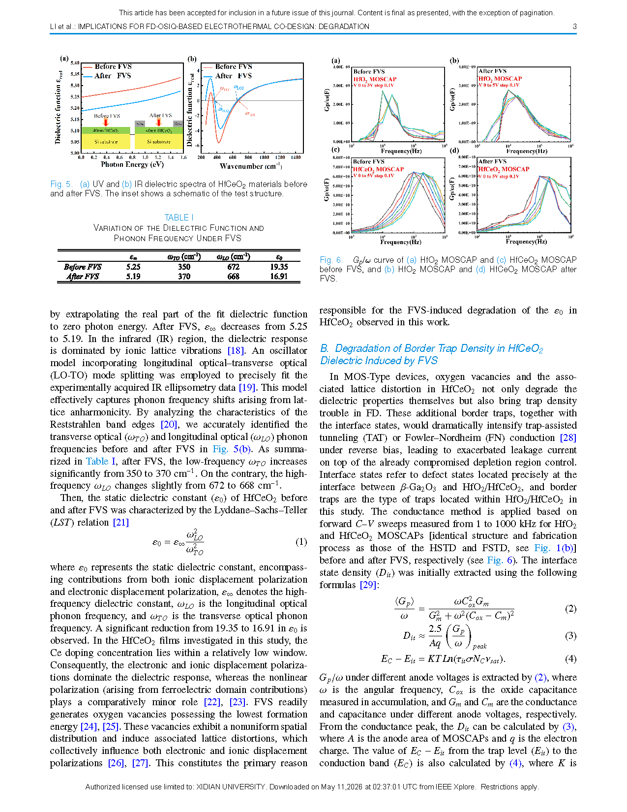
Fig. 3. Forward I–V characteristics of (a) HSTD and (b) FSTD before and after FVS.
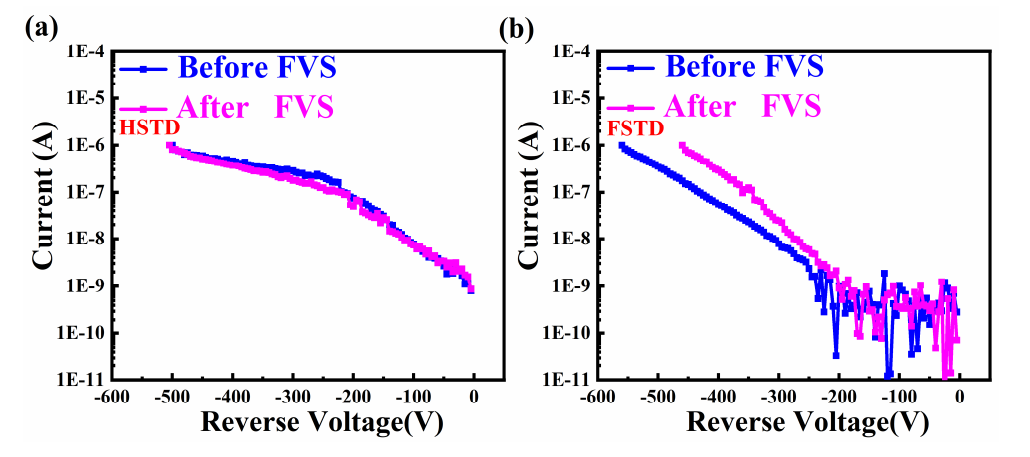
Fig. 4. Reverse I–V characteristics of (a) HSTD and (b) FSTD before and after FVS.
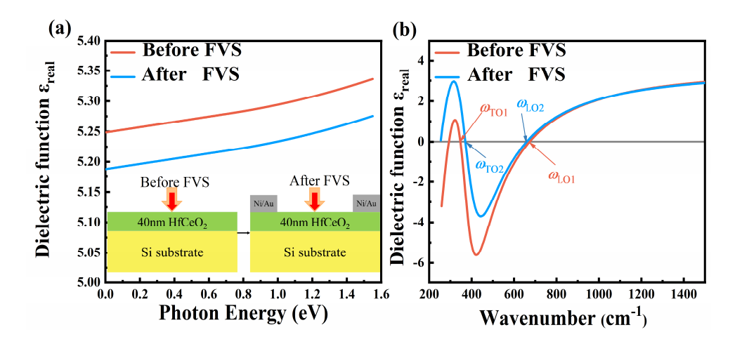
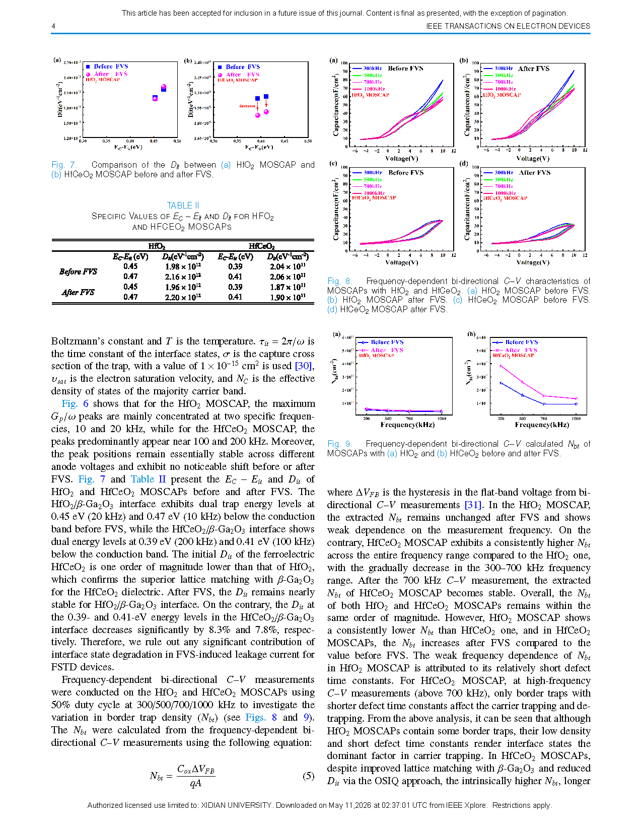
Fig. 5.(a) UV and (b) IR dielectric spectra of HfCeO₂ materials before and after FVS. The inset shows a schematic of the test structure.
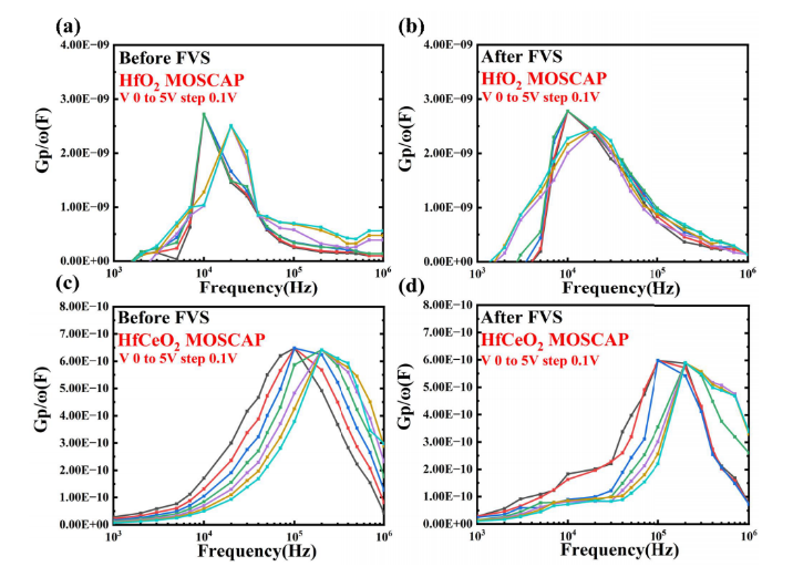
Fig. 6. Gp/w curve of (a) HfO₂ MOSCAP and (c) HfCeO₂ MOSCAP before FVS, and (b) HfO₂ MOSCAP and (d) HfCeO₂ MOSCAP after FVS.
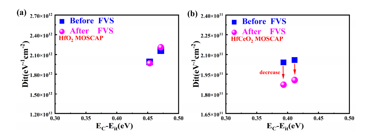
Fig. 7. Comparison of the Dit between (a) HfO₂ MOSCAP and (b) HfCeO₂ MOSCAP before and after FVS.
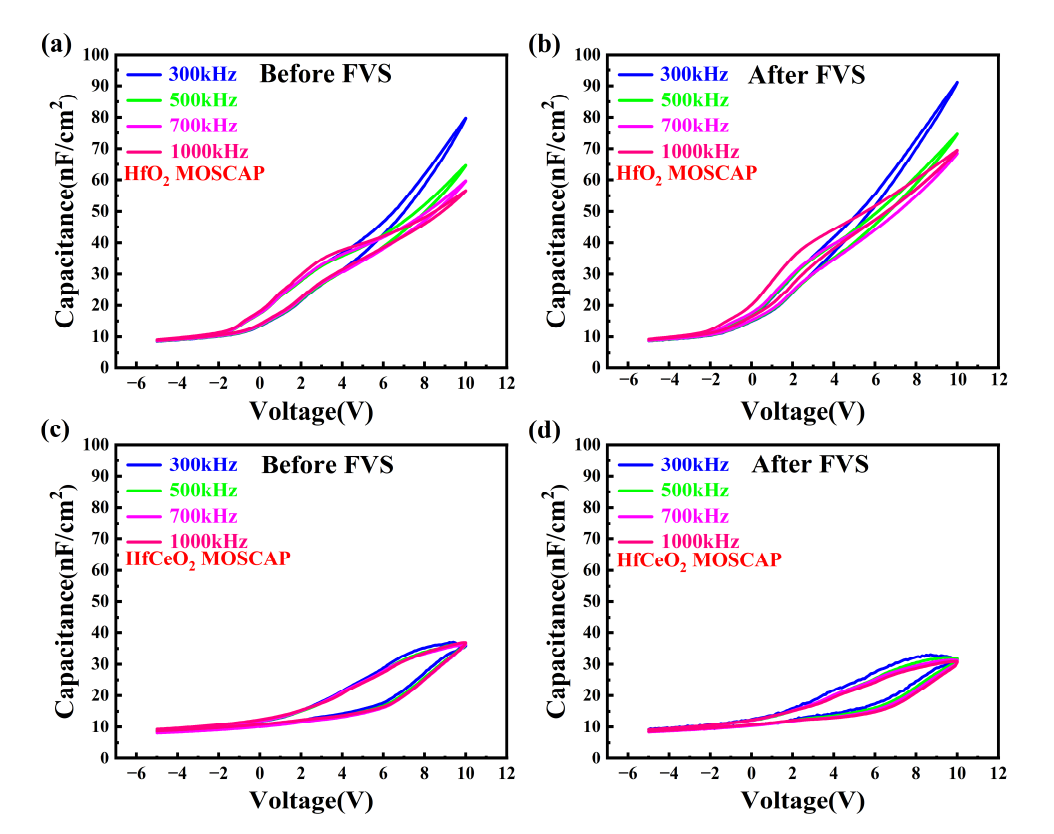
Fig. 8. Frequency-dependent bi-directional C–V characteristics of MOSCAPs with HfO₂ and HfCeO₂ .(a) HfO₂ MOSCAP before FVS. (c) HfCeO₂ MOSCAP before FVS. (b) HfO₂ MOSCAP after FVS. (d) HfCeO₂ MOSCAP after FVS.
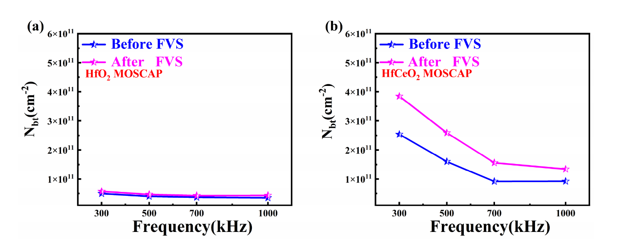
Fig. 9. Frequency-dependent bi-directional C–V calculated Nbt of MOSCAPs with (a) HfO₂ and (b) HfCeO₂ before and after FVS.
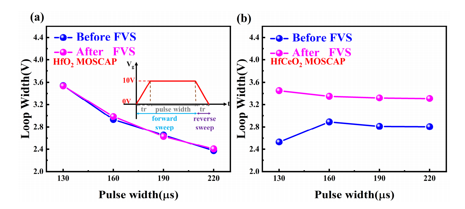
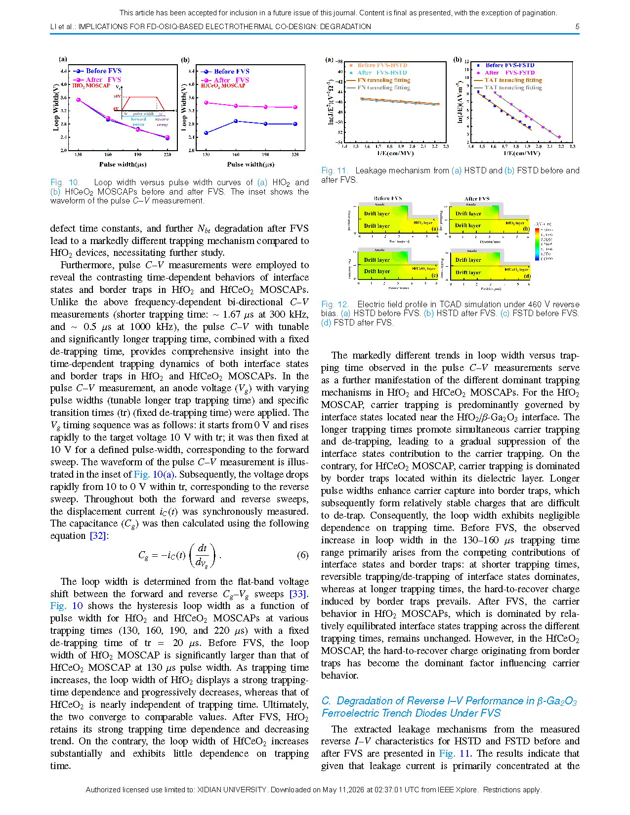
Fig. 10. Loop width versus pulse width curves of (a) HfO₂ and (b) HfCeO₂ MOSCAPs before and after FVS. The inset shows the waveform of the pulse C–V measurement.
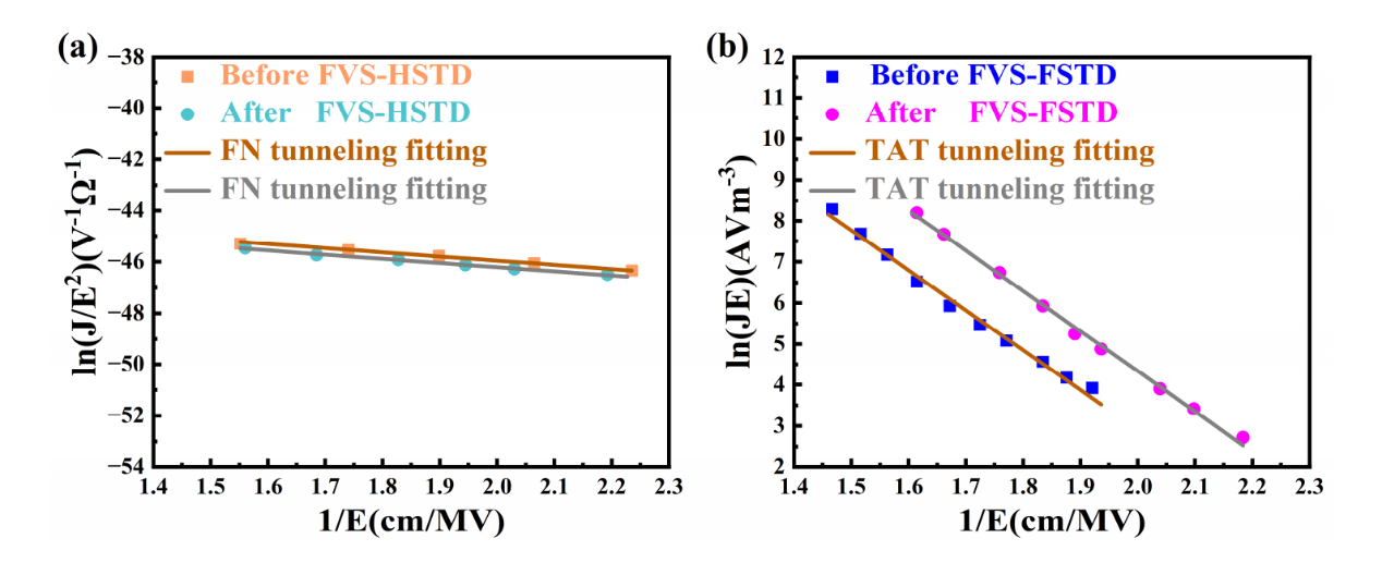
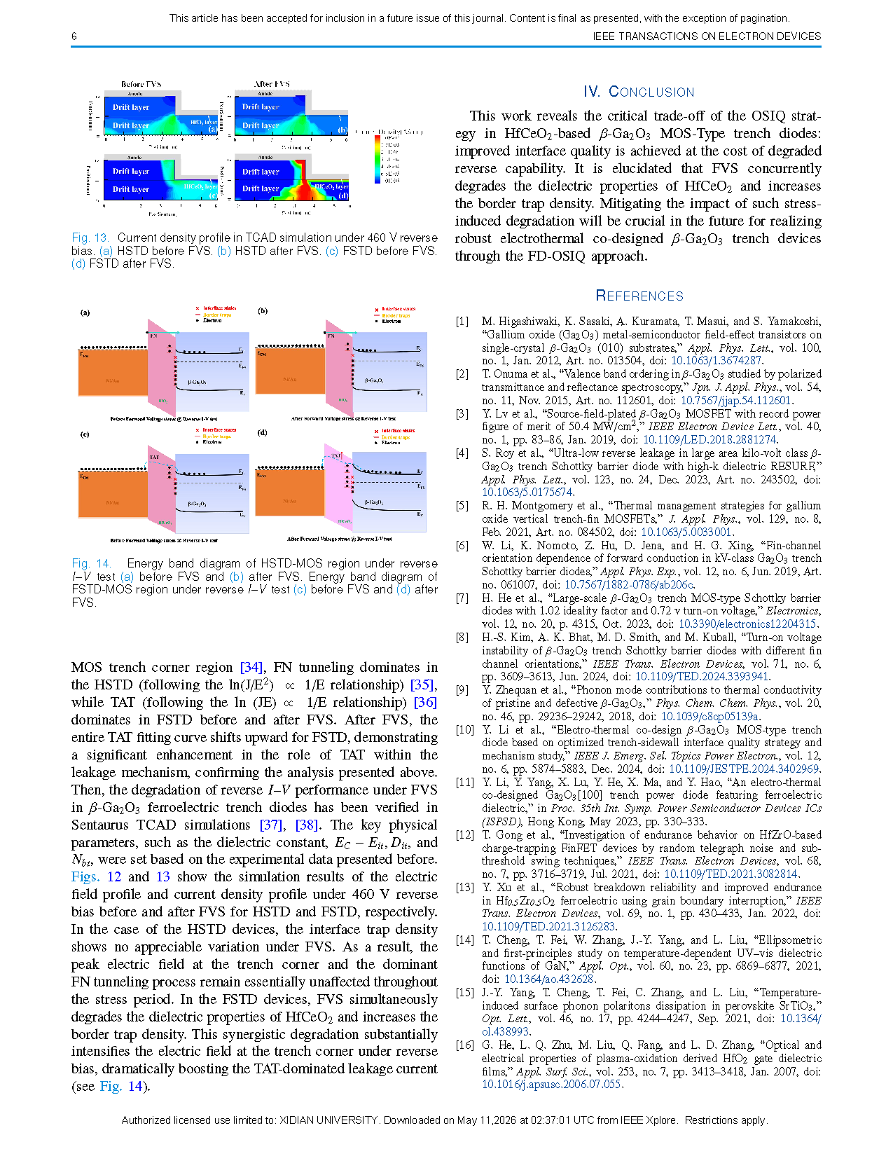
Fig. 11. Leakage mechanism from (a) HSTD and (b) FSTD before and after FVS. FN tunneling fitting TAT tunneling fitting.
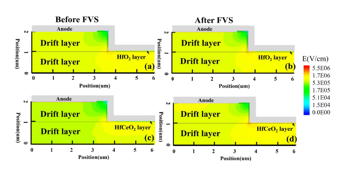
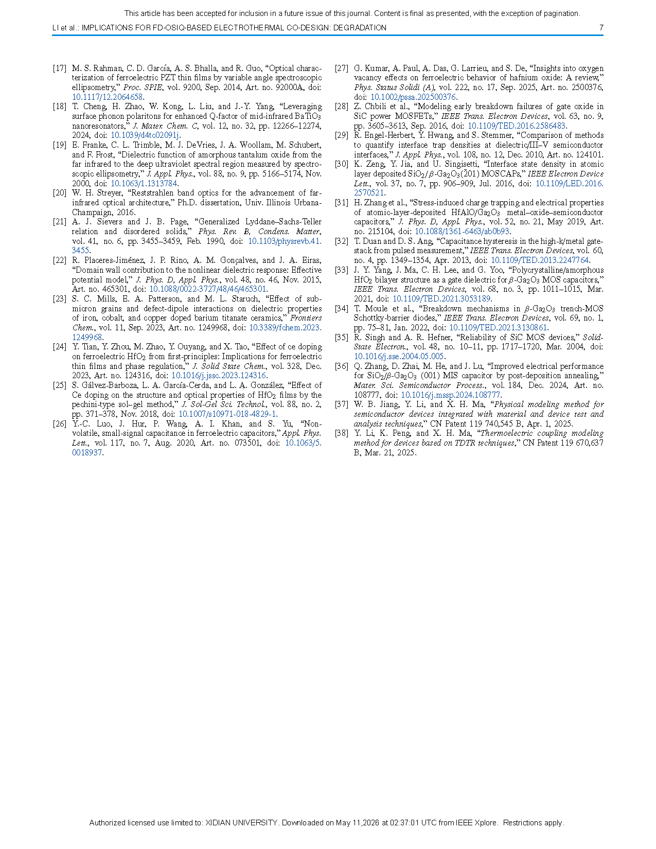
Fig. 12. Electric field profile in TCAD simulation under 460 V reverse bias. (a) HSTD before FVS. (b) HSTD after FVS. (c) FSTD before FVS. (d) FSTD after FVS.
DOI:
10.1109/TED.2026.3688208
Instruction
Official Account

Cooperation
Top
