


What are “defects” in materials?
In an ideal crystal, atoms are arranged in a perfectly periodic pattern, occupying every lattice site in a repeating order. In real materials, however, this periodicity is disrupted. Any deviation from the ideal periodic lattice arrangement is referred to as a defect.
Based on their geometry, defects are commonly classified into four categories: point defects, line defects, planar defects, and volumetric (bulk) defects. Among them, vacancies, interstitial atoms, and substitutional atoms are point defects. Dislocations are typical line defects. Grain boundaries, twin boundaries, and stacking faults belong to planar defects. Voids, second-phase particles, and defect clusters are categorized as bulk defects.
Defects are not exclusive to low-quality materials. Even at temperatures above absolute zero, a certain equilibrium concentration of vacancies exists within crystals, and this concentration increases exponentially with temperature, determined by the vacancy formation energy.
Processes such as quenching, cold working, thin-film deposition, and irradiation can introduce defect concentrations far exceeding the equilibrium level. During doping, foreign atoms may occupy lattice sites or interstitial positions, often accompanied by charge-compensating vacancies. A truly defect-free material does not exist at finite temperatures. The real question is not whether defects exist, but rather their concentration, size, distribution, and location—and how these factors influence specific material properties.
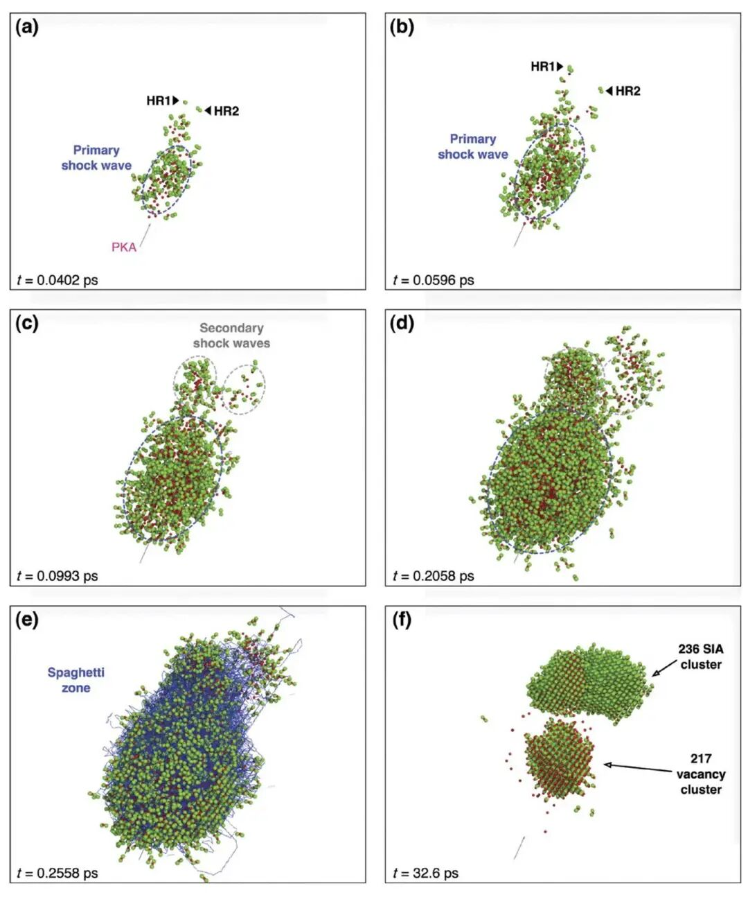 Figure 1. Defect generation process in molecular dynamics displacement cascade simulations, where red atoms represent vacancies and green atoms represent interstitial atoms. DOI: 10.3390/app15169110
Radiation-induced cascades are a typical mechanism for the generation of a large number of point defects. When high-energy particles impinge on a crystal, they displace atoms from their equilibrium lattice positions, producing primary radiation damage in the form of vacancy–interstitial pairs.
Subsequently, these point defects undergo migration, recombination, or further clustering within the material.
In metals, semiconductors, and oxides at room temperature, different types of vacancies and interstitials exhibit different migration energies. Defects with higher mobility are more likely to recombine with each other within a short time or be absorbed by structural sinks such as grain boundaries. In contrast, defects with lower mobility may persist within the crystal and gradually accumulate over time.
Interstitial atoms occupy the spaces between lattice sites, while substitutional atoms replace host lattice atoms. These different defect types also induce varying degrees of local lattice distortion compared to vacancies.
Ultimately, the defect concentration in a material is determined by a dynamic balance between defect production and annihilation rates.
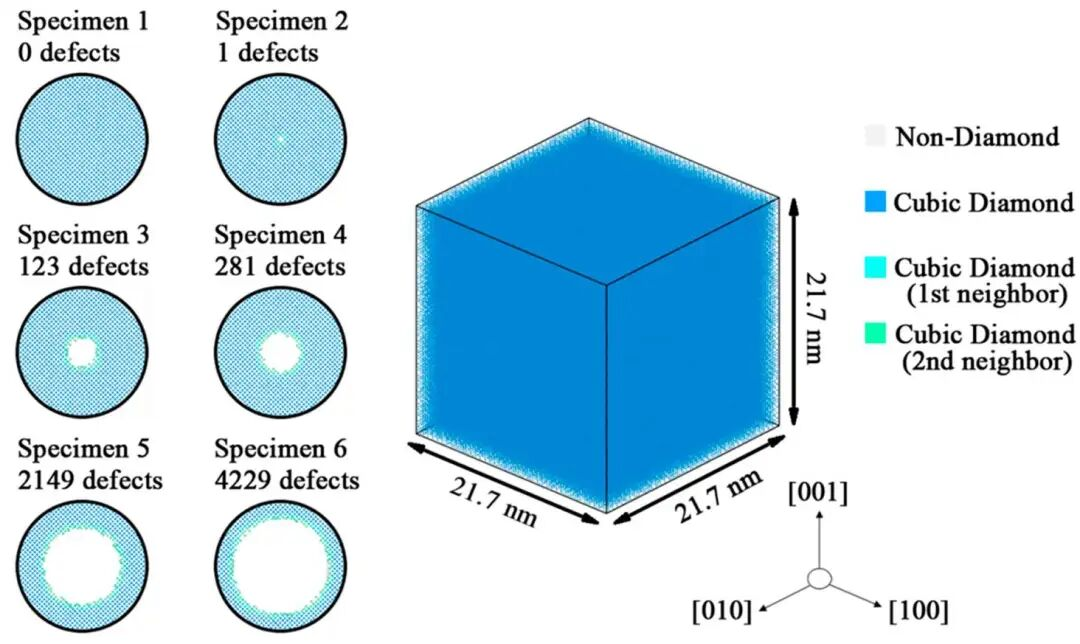
Figure 2. Unit cell model of single-crystal silicon and six simulation cases containing point defects of different sizes. DOI: 10.3390/ma14113011
To place point defects in a specific crystal, one can develop a more intuitive understanding of their spatial scale. Taking covalent crystals such as single-crystal silicon as an example, when a small cluster of atoms is locally missing, a vacancy-type defect region is formed. As the spatial extent of the defect increases, the associated distortions in bond lengths and bond angles around the defect also expand, leading to increasingly significant perturbations in the material’s mechanical behavior and electronic structure.
The influence of defects on material properties is not governed by a single factor. Instead, it results from the combined effects of defect type, size, concentration, and spatial distribution, which together determine whether defects play a beneficial or detrimental role in a given property. Based on this, the discussion can be further extended to mechanical, electrical, optical, ionic transport, and thermal properties in the following sections.
Why can defects improve certain material properties?
One of the most important ways defects enhance material performance is through ionic transport. When ions migrate in a solid, they typically rely on vacancies as “hopping sites” to complete the diffusion process. For example, in yttria-stabilized zirconia, doping with lower-valence cations such as yttrium introduces oxygen vacancies to maintain overall charge neutrality. Oxygen ions then migrate by hopping through these vacancies within the fluorite lattice. The fundamental conduction mechanism in solid oxide fuel cell electrolytes is essentially this vacancy-mediated diffusion process.
The concentration of vacancies can be directly tuned through the doping level, meaning ionic conductivity can be engineered within a controllable range. In lithium- or sodium-ion solid electrolyte systems, migration also depends on cation vacancies or related defect structures that provide diffusion pathways. Without sufficient vacancies, ion transport becomes strongly restricted, and conductivity cannot be effectively improved.
In electrical properties, defects also play a critical regulatory role. Taking silicon as an example, phosphorus doping introduces donor energy levels, while boron doping introduces acceptor levels. These defect-induced states directly modify carrier concentration, thereby tuning electrical conductivity. Modern semiconductor devices are fundamentally based on this controllable doping mechanism, where conductivity can vary over several orders of magnitude with doping concentration. In metallic systems, an appropriate amount of vacancies and dislocations can influence electron scattering and atomic diffusion, thereby affecting resistivity and further impacting processes such as age hardening and diffusion bonding.
In luminescent materials, the role of defects becomes even more “functional.” Oxygen vacancies, color centers, and rare-earth activator centers introduce localized energy levels within the bandgap. Electronic transitions between these defect states can generate emission at specific wavelengths.
In phosphor systems, modifying the host composition can tune the local crystal field environment around defect centers, thereby affecting emission wavelength, intensity, and thermal stability. For example, changes in Ca content within the host lattice lead to shifts in both spectral intensity and spectral shape under different temperatures, clearly demonstrating how defect environments govern luminescence behavior.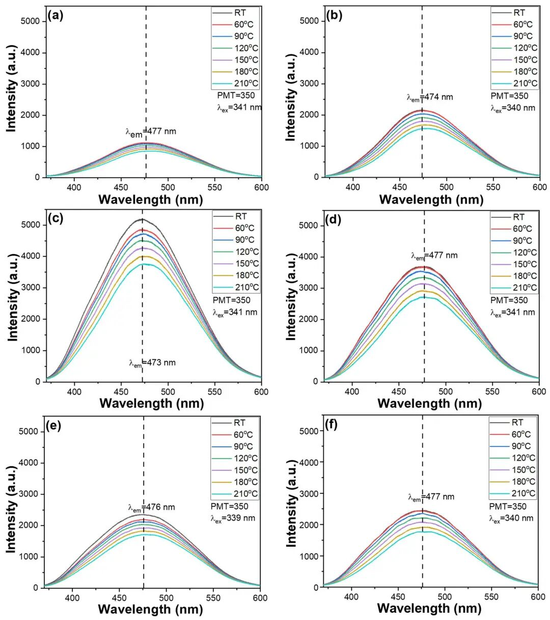
Figure 3. Temperature-dependent emission spectra of Ca–Ga–O-based phosphors with different Ca concentrations. DOI: 10.3390/photonics12070625
From a mechanical perspective, at the nanoscale, vacancies, dislocations, and second-phase particles can all act as pinning centers for dislocation motion, thereby impeding slip processes and increasing the strength and hardness of materials. The essence of work hardening and precipitation strengthening lies in this obstruction of dislocation migration.
In thermoelectric materials, point defects are often intentionally introduced to scatter phonons, thereby reducing lattice thermal conductivity, while minimizing adverse effects on charge transport. This strategy ultimately improves the thermoelectric figure of merit (ZT). In this context, defects are not unwanted “impurities” that need to be eliminated, but rather functional units deliberately engineered and utilized. The key lies in precisely controlling their type, concentration, and spatial distribution.
Why can “more defects” actually degrade performance?
The key reason is that the same type of defect can produce fundamentally different—and even opposite—effects depending on its concentration. When the defect density increases beyond a certain threshold, the original strengthening mechanisms can transition into degradation mechanisms.
For example, molecular dynamics simulations of single-crystal silicon show that as the spatial extent of point defects increases, the yield strength decreases exponentially. This occurs because defect regions significantly enhance stress concentration, making crack nucleation easier and promoting earlier crack propagation, ultimately leading to premature fracture.
In brittle materials, voids and microcracks often serve as initiation sites for fracture. Moreover, the distribution of defect sizes further affects the statistical variability of material strength. Larger defect scales not only lead to more pronounced strength degradation but also increase the uncertainty of failure behavior. This is clearly reflected in silicon wafer processing, where phenomena such as edge chipping and microcrack formation are typical consequences of defect-driven fracture processes.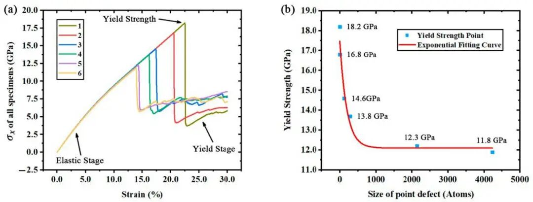
Figure 4. Stress–strain curves for different simulation cases and the exponential fitting relationship between yield strength and point defect size. DOI: 10.3390/ma14113011
Dislocations also exhibit a dual nature. At low densities, dislocations can interact and pin each other, thereby strengthening the material. However, when the dislocation density becomes too high, they begin to entangle, which reduces plasticity and leads to embrittlement.
Similarly, when the concentration of vacancies becomes excessive, they no longer remain isolated point defects; instead, they aggregate into voids or stacking-fault tetrahedra, resulting in volumetric swelling and accumulated damage. The clustering of vacancies is particularly pronounced under irradiation conditions.
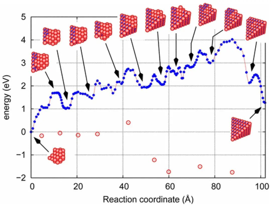
Figure 5. Evolution pathway of vacancy clusters from void-like structures to stacking-fault tetrahedra (SFT). DOI: 10.3390/app15169110
Electrical and optical properties are typically highly sensitive to excessive defect concentrations. As the number of defects increases, carrier scattering becomes stronger, leading to a reduction in carrier mobility. When defect-related energy levels act as non-radiative recombination centers, photogenerated carriers recombine before contributing effectively to transport, resulting in reduced luminescence efficiency or even complete quenching, thereby significantly degrading the performance of solar cells and light-emitting diodes.
The same defect state can exhibit entirely different roles depending on its concentration: at low densities, it may function as an efficient luminescence center, whereas at high densities it can become a dominant recombination center that severely suppresses device efficiency.
Ionic conductivity also exhibits an optimal window. Once the vacancy concentration exceeds a certain threshold, interactions between vacancies lead to correlation effects, ordering, or even clustering, which obstruct migration pathways and reduce ion mobility. Consequently, ionic conductivity decreases after reaching a peak value. In addition, when grain boundary density becomes too high, phonon scattering is enhanced across a broad frequency range, reducing thermal conductivity; however, carrier transport is also strongly hindered by grain boundaries, resulting in simultaneous degradation of electrical transport. Therefore, in thermoelectric materials, achieving both low thermal conductivity and high electrical conductivity is often intrinsically challenging.
What is the “optimal defect window” for different material properties?
In most materials, the relationship between defect concentration and performance is not monotonic, but rather exhibits a peak-shaped dependence, meaning there exists an optimal defect concentration range. For example, in doped zirconia systems, the oxygen ionic conductivity reaches a maximum when the oxygen vacancy concentration is around ~4%. Beyond this level, further doping leads to interactions between vacancies and a gradual tendency toward ordering, which restricts ion migration pathways and causes conductivity to decrease.
This peak position is typically governed by the strength of vacancy–vacancy interactions and whether the system undergoes ordering transitions at a given temperature. Therefore, it is incorrect to assume that “more vacancies always lead to higher conductivity.” Similar concentration-dependent maxima are also observed in fluoride ion conductors and proton conductors, where the optimal doping level varies with crystal structure and operating temperature.
In thermoelectric materials, this “optimal window” is even more constrained, as it requires simultaneous optimization of multiple competing parameters. The ideal carrier concentration is typically in the range of ~10¹⁹–10²⁰ cm⁻³, while the defect concentration must be carefully balanced to reduce lattice thermal conductivity without excessively scattering charge carriers. Deviations from this window lead to a reduction in the thermoelectric figure of merit (ZT). In essence, defect engineering is fundamentally a multi-constraint optimization problem. When the carrier concentration becomes too high, electrical conductivity may improve, but the Seebeck coefficient decreases, ultimately reducing the power factor.
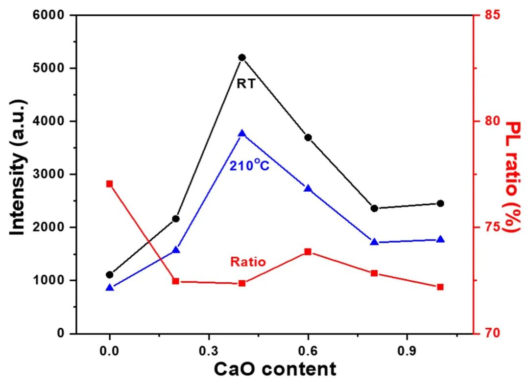
Figure 6. Variation of maximum emission intensity at room temperature and 210 °C, and their ratio as a function of Ca content. DOI: 10.3390/photonics12070625
In luminescent materials, if the concentration of activators or defect-related centers is too low, the number of emission centers becomes insufficient, resulting in weak overall luminescence. However, when the concentration becomes too high, concentration quenching occurs, leading to a decrease in emission intensity. Therefore, such systems typically exhibit an optimal doping range.
Taking phosphors as an example, by tuning the Ca composition, one can identify a condition where the ratio of room-temperature to high-temperature emission intensity is maximized, achieving a balance between brightness and thermal stability. This type of property evolution with composition typically follows a single-peaked curve, reaching an optimum at a specific doping level.
From a mechanical perspective, the optimal state is more strongly governed by the size and spatial distribution of defects. Finely dispersed defects facilitate dislocation pinning, thereby enhancing strength, whereas large voids or defect clusters tend to degrade mechanical performance.
Even at identical overall defect densities, differences in spatial distribution can lead to markedly different mechanical responses: uniformly distributed defects generally result in higher strength than locally aggregated ones. In many cases, therefore, the key determinant is not simply the defect concentration, but also the defect size, distribution, and location.
It should be emphasized that this concept of an “optimal window” is always defined with respect to a specific property and under specific operating conditions. When the performance target or service environment changes, the position and range of the optimal defect window will also shift accordingly.
How to determine the quantity, type, and location of defects?
To accurately determine the type, quantity, and spatial distribution of defects, a combination of complementary characterization techniques is required. Each method provides a different “view” of the defect landscape, from long-range averages to atomic-scale imaging.
X-ray diffraction (XRD) probes the long-range averaged crystal structure. Shifts in peak positions are typically associated with lattice parameter changes induced by point defects or solid-solution effects, while peak broadening reflects increased dislocation density and microstrain. Through Williamson–Hall analysis, it is possible to separate the contributions of crystallite size and strain. However, XRD mainly provides statistical information over a large volume and cannot directly locate individual defects.
Transmission electron microscopy (TEM) and aberration-corrected electron microscopy (AC-TEM) allow direct imaging of dislocations, stacking faults, voids, and defect clusters, with resolution down to the atomic column level. The limitation, however, is their relatively small sampling volume, which reduces statistical representativeness when extrapolating to the bulk material.
Positron annihilation spectroscopy is particularly sensitive to vacancy-type defects. It can provide quantitative information on vacancy concentration and size, making it highly effective for detecting open-volume defects that are difficult to resolve structurally.
In summary, TEM-based techniques are primarily used for morphological and structural visualization, positron-based methods are powerful for vacancy characterization, while XRD provides ensemble-averaged structural and strain information. A complete understanding of defect chemistry and local environment typically requires integrating multiple methods rather than relying on a single technique.
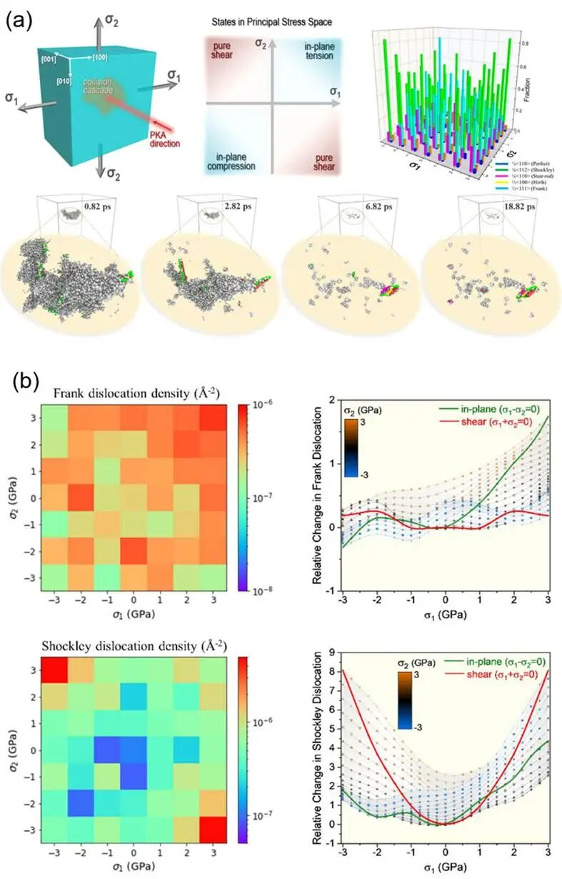
Figure 7. Types and distributions of dislocation loops induced by irradiation under different stress states. DOI: 10.3390/app15169110
Electron paramagnetic resonance (EPR) responds only to defects containing unpaired electrons. Oxygen vacancies, F-centers, and free radicals produce characteristic signals. Photoluminescence and time-resolved spectroscopy reflect trap energy levels and non-radiative recombination rates.
In Raman spectroscopy, defect-activated vibrational modes—such as the D band in carbon materials—have intensities that correlate with defect density. Annealing studies can track the recovery of defect-related signals with temperature, helping distinguish defects with different migration energies.
Electrical measurements provide complementary information from another perspective. Hall effect and conductivity measurements vary with defect concentration, allowing tracking of carrier density and mobility changes.
By correlating structural imaging, spectroscopic signals, and transport properties on the same set of samples, one can distinguish defect types, quantities, and spatial distributions.
Oxygen vacancy concentration, dislocation density, and grain boundary area all vary with synthesis conditions, leading to corresponding changes in electrical conductivity, yield strength, and luminescence intensity. Whether defects are beneficial or detrimental ultimately depends on measurable, quantitative parameters.
Instruction
Official Account

Cooperation
Top
