


Researchers from Suzhou Institute of Nano-Tech and Nano-Bionics, Chinese Academy of Sciences and Henan Normal University have published a dissertation titled “Internal Field Optimization Using a Localized Bottom SiO₂ in Vertical β-Ga₂O₃ FinFETs“ in 2026 IEEE 38th International Symposium on Power Semiconductor Devices and ICs (ISPSD).
Background
The booming development of electric vehicles, renewable energy conversion and data center power supplies puts forward higher requirements for power transistors with high breakdown voltage, low conduction loss and stable operation under high electric field. Ultra-wide bandgap semiconductors have superior performance owing to their large bandgap and high critical breakdown electric field. As a representative material, β-Ga₂O₃ has a bandgap of 4.8–4.9 eV and a theoretical critical electric field of 8 MV/cm, and large-size single crystal substrates can be fabricated, making it highly suitable for high-voltage power switching devices.
Vertical β-Ga₂O₃ Schottky barrier diodes have been well developed, while the lack of feasible p-type doping hinders the application of conventional enhancement-mode MOSFETs based on p-n junctions. Vertical FinFETs can realize normally-off operation without p-type doping. However, severe electric field crowding at the trench corners of fin channels causes premature breakdown, which limits the reverse blocking capability and device reliability. A localized dielectric internal field optimization structure is proposed in this work to regulate the internal electric field distribution.
Abstract
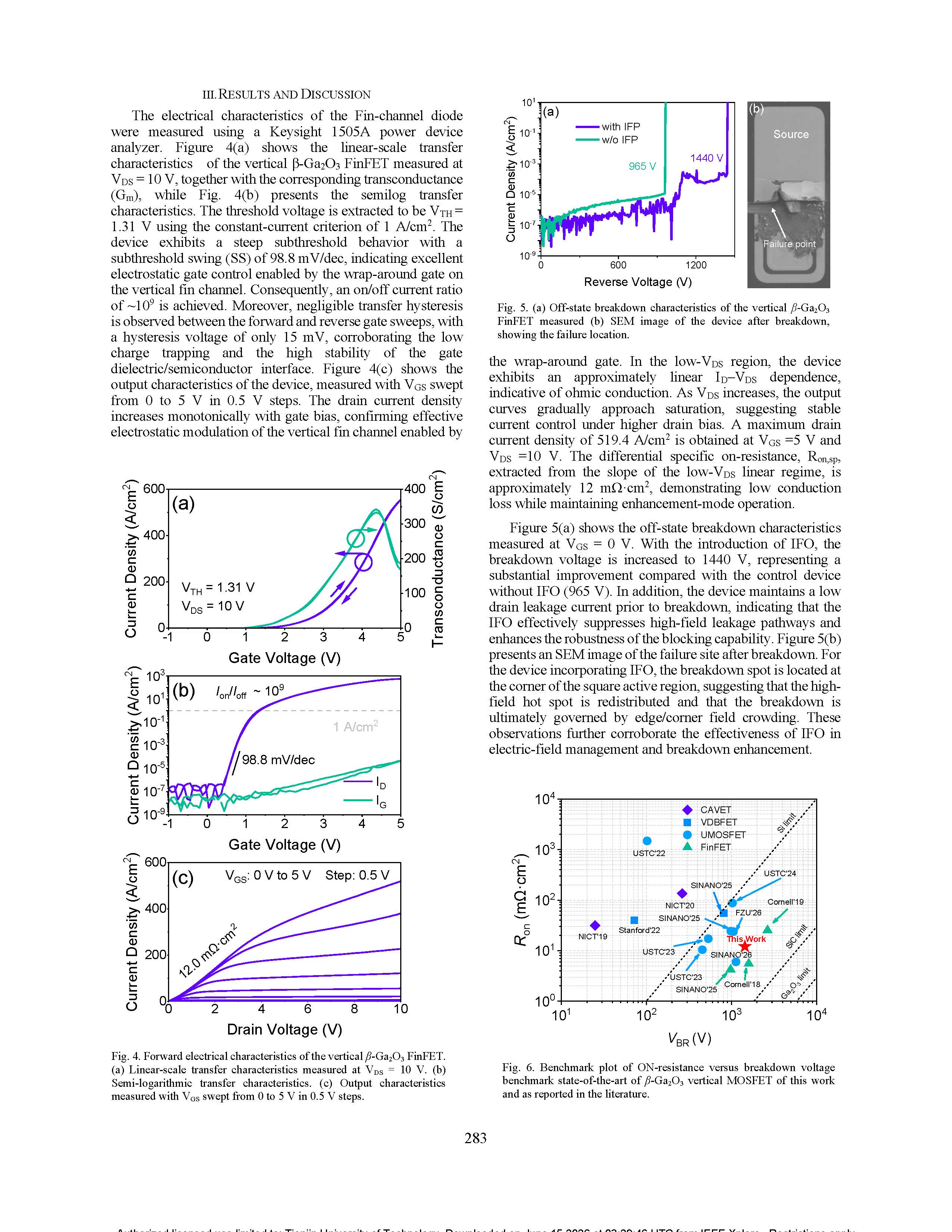
Vertical β-Ga₂O₃ FinFETs are promising candidates for high-voltage power switching because they enable normally-off operation through geometric depletion while leveraging the ultra-wide bandgap for high electric-field blocking. However, premature breakdown can still be triggered by severe electric-field crowding at the trench bottom corners. In this work, we demonstrate a vertical β-Ga₂O₃ FinFET with enhanced reverse blocking enabled by an internal field-optimization (IFO) structure, realized by introducing an 100nm SiO₂ dielectric liner locally at the fin bottom/corner regions. Owing to the dielectric field management, the device achieves a breakdown voltage of 1440 V, representing a substantial improvement over the control device without IFO. The FinFET exhibits enhancement-mode characteristics with VTH=1.31 V, a subthreshold swing of 98.8 mV/dec, an on/off current ratio of 10⁹, and a strongly suppressed transfer hysteresis of 15 mV. A maximum drain current density of 519.4 A/cm², with a differential specific on-resistance (Ron, sp) 12 mΩ·cm². These results highlight dielectric-assisted corner field shaping as a practical route toward simultaneously improving breakdown robustness and maintaining low conduction loss in vertical β-Ga₂O₃ FinFET power transistors.
Highlights
A novel internal field optimization structure with localized 100 nm SiO₂dielectric at fin bottom and corners is proposed to relieve electric field crowding, which is fully compatible with existing fabrication processes.
The breakdown voltage is increased from 965 V to 1440 V with low leakage current before breakdown, and the reverse blocking capability is greatly improved.
The device retains excellent enhancement-mode performance, including proper threshold voltage, low subthreshold swing and tiny transfer hysteresis.
The device achieves low specific on-resistance and high drain current density, with a Baliga figure of merit of 137 MW/cm², showing excellent trade-off between conduction loss and blocking voltage.
The breakdown position transfers to the edge of active region, which verifies the effective electric field regulation of the proposed structure.
Conclusion
In conclusion, we show that localized corner-dielectric field shaping is an effective and process-compatible approach to improve the blocking robustness of vertical β-Ga₂O₃ FinFETs. By introducing an 100nm SiO₂ IFO at the fin bottom/corner regions, the breakdown voltage increases from 965 V to 1440 V while maintaining low pre-breakdown leakage. Post-breakdown SEM indicates that the failure shifts to the perimeter corner of the square active region, consistent with suppressed internal trench-bottom field crowding. The device preserves enhancement-mode operation and strong forward conduction, suggesting that further improvements are achievable by co-optimizing external edge termination with the internal dielectric liner.
Project Support
This work was supported in part by the National Natural Science Foundation of China (Nos. 62074053), in part the Key Scientific Research Project in Colleges and Universities of Henan Province (Grant No. 26B140020), the Natural Science Foundation of Henan (Grant No. 252300423347), in part by the Funded by Basic Research Program of Jiangsu (Grant No. BK20253003), in part by the Suzhou Critical Core Technology Research Project (Grant No. SYG2024003). The authors would like to thank Nano Fabrication Facility and Vacuum Interconnected Nanotech Workstation (NANO-X) of Suzhou Institute of Nano-Tech and Nano-Bionics, Chinese Academy of Sciences for their technical support.
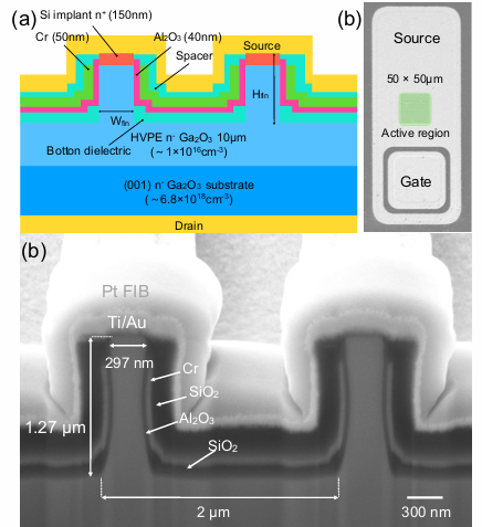
Figure 1 (a) Schematic illustration of the bottom-filled multi-fin vertical β-Ga₂O₃ FinFET. (b) Top-view SEM image of the fabricated device. (c) Cross-sectional SEM image of a representative device with a designed fin width of 300 nm.
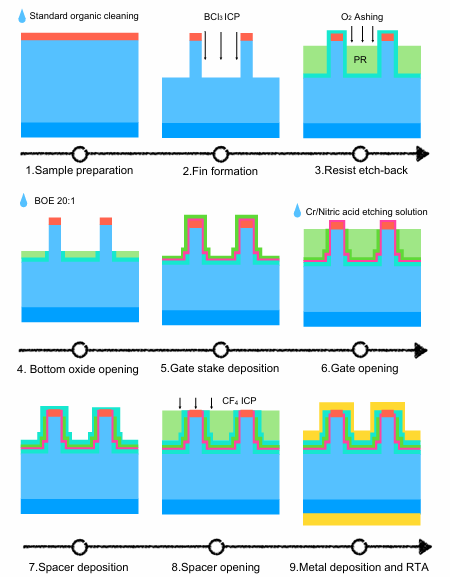
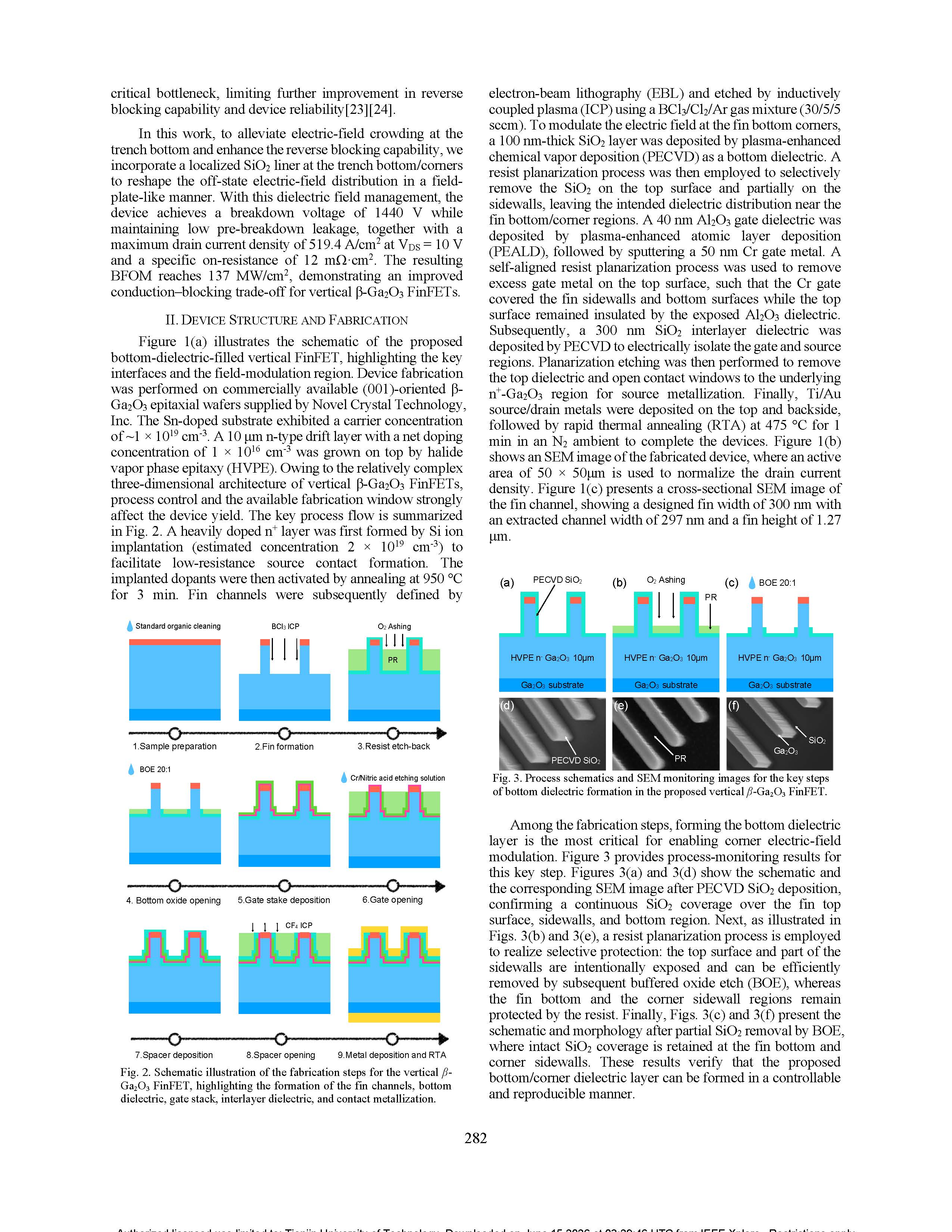
Figure 2 Schematic illustration of the fabrication steps for the vertical β-Ga₂O₃ FinFET, highlighting the formation of the fin channels, bottom dielectric, gate stack, interlayer dielectric, and contact metallization.
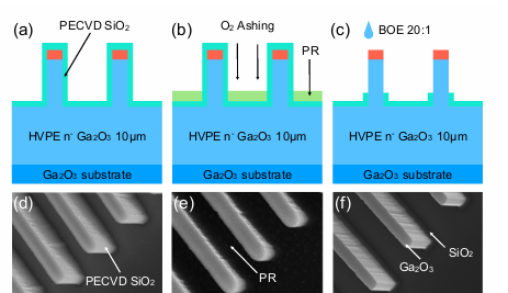
Figure 3 Process schematics and SEM monitoring images for the key steps of bottom dielectric formation in the proposed vertical β-Ga₂O₃ FinFET.
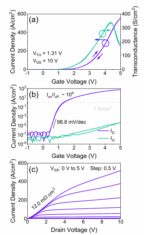
Figure 4 Forward electrical characteristics of the vertical β-Ga₂O₃ FinFET. (a) Linear-scale transfer characteristics measured at VDS=10 V. (b) Semi-logarithmic transfer characteristics. (c) Output characteristics measured with VGS swept from 0 to 5 V in 0.5 V steps.
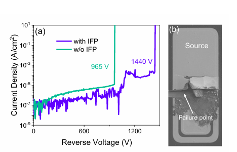
Figure 5 (a) Off-state breakdown characteristics of the vertical β-Ga₂O₃ FinFET measured (b) SEM image of the device after breakdown, showing the failure location.
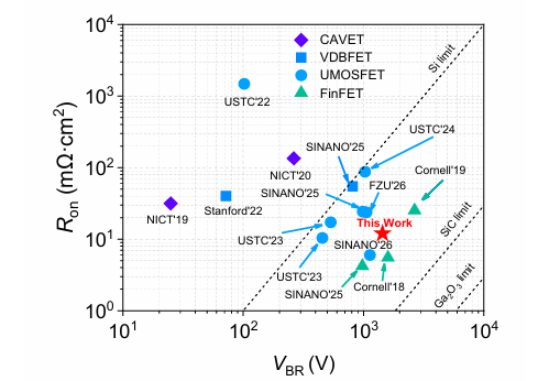
Figure 6 Benchmark plot of ON-resistance versus breakdown voltage benchmark state-of-the-art of β-Ga₂O₃ vertical MOSFET of this work and as reported in the literature.
DOI:
10.1109/ISPSD64561.2026.11553619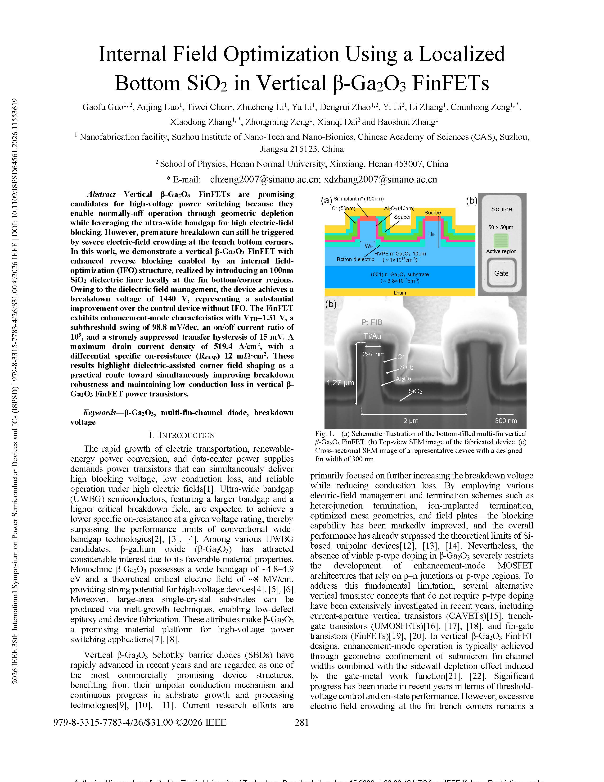
Instruction
Official Account

Cooperation
Top
