


Researchers from The Pennsylvania State University and Luxium Solutions, LLC have published a dissertation titled "Evaluation of surface preparation methods for epitaxial growth on miscut (100) β-Ga₂O₃ substrates" in Applied Surface Science.
Background
Beta-gallium oxide (β-Ga₂O₃) is an ultra-wide bandgap semiconductor with bandgap of 4.85 eV and critical electric field of 8 MV/cm, suitable for high-power electronic devices, sensors and optoelectronics. Large-size single crystals can be mass-produced via melt growth methods such as EFG and vertical Bridgman. Miscut (100) substrates can suppress twin defects and 2D island nucleation during epitaxy, realizing step-flow growth and high carrier mobility, which makes them promising substrates.
Traditional surface processes using phosphoric acid etching plus O₂ annealing only work for Mg-doped insulating substrates, while severe surface roughening occurs on Fe-doped insulating and Sn-doped conductive substrates. The optimal etching and annealing recipes for different dopant types remain unclear. Annealing atmosphere, pressure, temperature and duration modulate gallium vacancy concentration, altering surface step ordering and substrate conductivity; Si contamination also destroys terrace-step structures.
This work systematically compares three etchants (HF, TMAH, phosphoric acid) and diverse Ar/O₂ annealing conditions on surface morphology and electrical properties of two substrate types. Universal pretreatment processes for both insulating and conductive miscut (100) β-Ga₂O₃ are established, providing manufacturable in-situ treatment recipes before MOCVD/HVPE epitaxy.
Abstract
Miscut (100) gallium oxide (β-Ga₂O₃) substrates have emerged as an attractive orientation for growth of homoepitaxial layers with a low defect density, smooth surface morphology, and comparatively high mobility. While previous studies used phosphoric acid (H₃PO₄) etching and O₂ annealing to prepare Mg-doped, miscut (100) substrates for epitaxial growth, significant surface roughening was observed when implementing these conditions for substrates with other dopant types in this work. The surface preparation steps were systematically evaluated for both insulating, Fe-doped and conductive, Sn-doped β-Ga₂O₃ substrates. A smooth surface topography (Sq / rms<0.2 nm) with uniform step edges was obtained after annealing each type of substrate at 850-900°C in a pressure range achievable with typical vapor-phase epitaxy systems. By keeping the O₂ partial pressure (PO₂) sufficiently low during the annealing step, surface conductivity was also maintained for the Sn-doped substrates. Comparing the annealing results with previous density functional theory (DFT) and experimental defect studies, this work suggests that the surface step formation and overall ordering mechanism is influenced by the concentration of Ga vacancies (VGa) and impurities that can occupy, form defect complexes, and/or diffuse via these sites. Further reduction in the average surface roughness (Sq / rms<0.15 nm) was also demonstrated using a dilute tetramethylammonium hydroxide (TMAH) etching step prior to annealing. Following surface preparation, epitaxial growth was demonstrated on the miscut (100) substrates with a growth rate of >2 μm / hour and an average surface roughness of ~0.6 nm Sq/rms. Overall, this study establishes processes for preparing both insulating and conductive, miscut (100) β-Ga₂O₃ substrates with vicinal surfaces suitable for epitaxial growth.
Highlights
This work systematically compares H₃PO₄, HF, TMAH etchants and multiple annealing recipes on both Fe-doped insulating and Sn-doped conductive miscut (100) β-Ga₂O₃substrates for the first time.
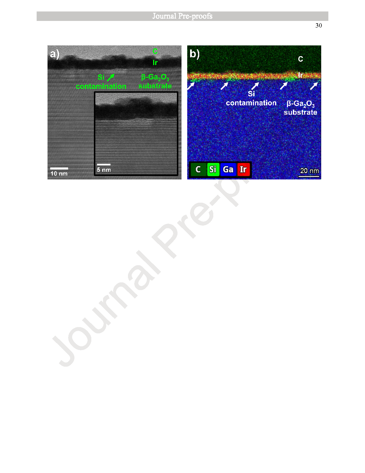
Verifies that traditional H₃PO₄+ O₂ annealing fails for Fe/Sn-doped wafers; high O₂ pressure annealing generates Si impurity particles and destroys terrace-step morphology.
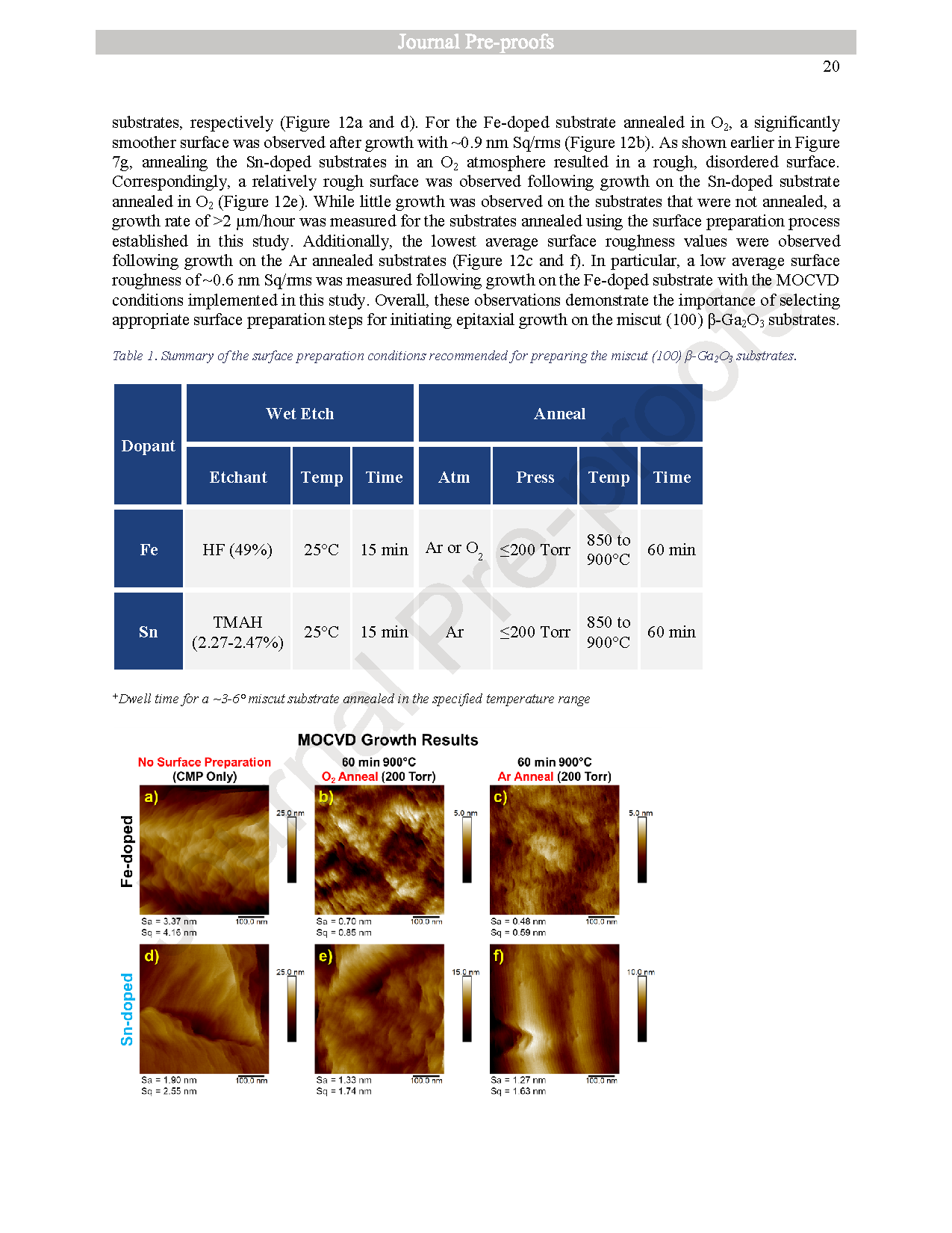
Confirms optimal recipe for Sn conductive substrates: 850–900 °C annealing under 200 Torr low-pressure Ar atmosphere, which suppresses Ga vacancy formation and retains surface conductivity.
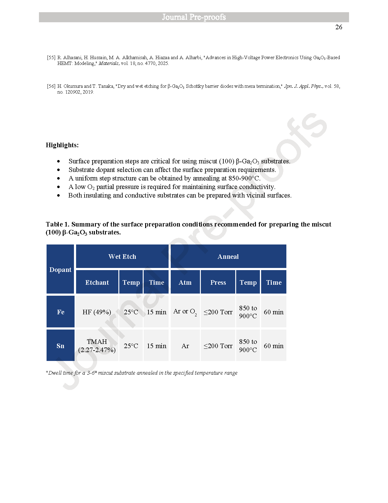
Proposes dilute TMAH pre-etching process, reducing substrate Sq roughness below 0.15 nm after annealing, better than HF etching.
Elaborates the co-regulation mechanism of Ga vacancies and Si impurities on surface step ordering; MOCVD epitaxy verification is realized with growth rate >2 μm/h and epilayer roughness ~0.6 nm.
Conclusion
In this study, etching and annealing conditions were systematically evaluated to identify conditions for preparing a smooth surface with a uniform step/terrace structure for facilitating step-flow epitaxial growth on miscut (100) β-Ga₂O₃ substrates. In particular, annealing conditions that can be feasibly implemented in typical MOCVD/HVPE reactors were selected to enable in-situ processing immediately prior to epitaxial growth. Surface preparation conditions were evaluated for both insulating, Fe-doped and conductive, Sn-doped substrates. It was observed that the dopant selection can significantly affect the surface topography of miscut (100) β-Ga₂O₃ substrates when using the same surface preparation steps. While previous studies implemented a H₃PO₄ etch followed by an O₂ anneal for Mg-doped substrates prior to epitaxial growth, this process resulted in a large increase in the average surface roughness for substrates with other dopant types. Significant surface contamination was also observed when annealing at higher pressures, which was identified to be primarily Si. However, by selecting appropriate surface preparation conditions, a smooth surface with a well-defined step/terrace structure was achieved for the substrates.
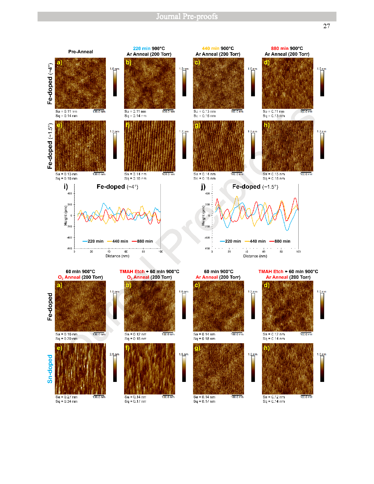
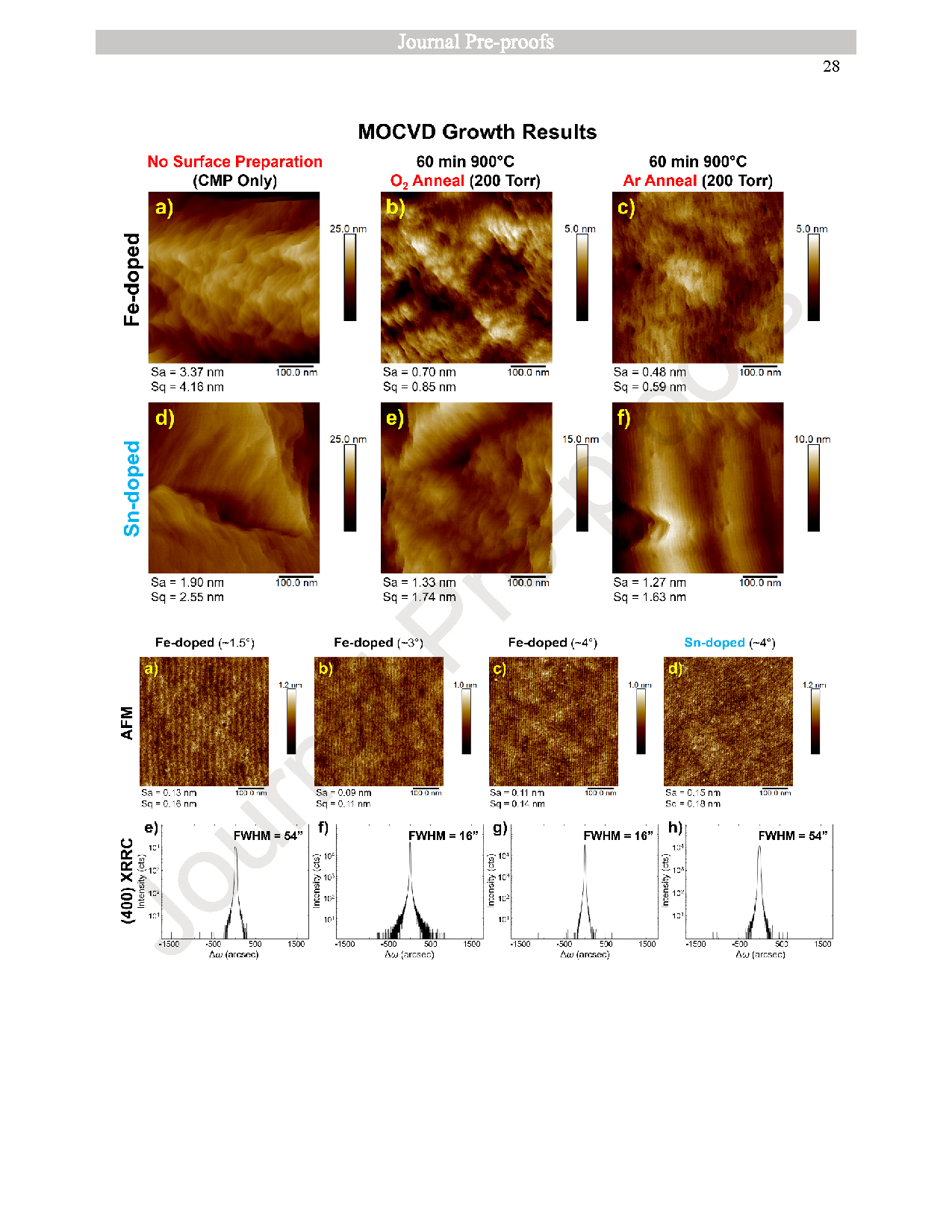
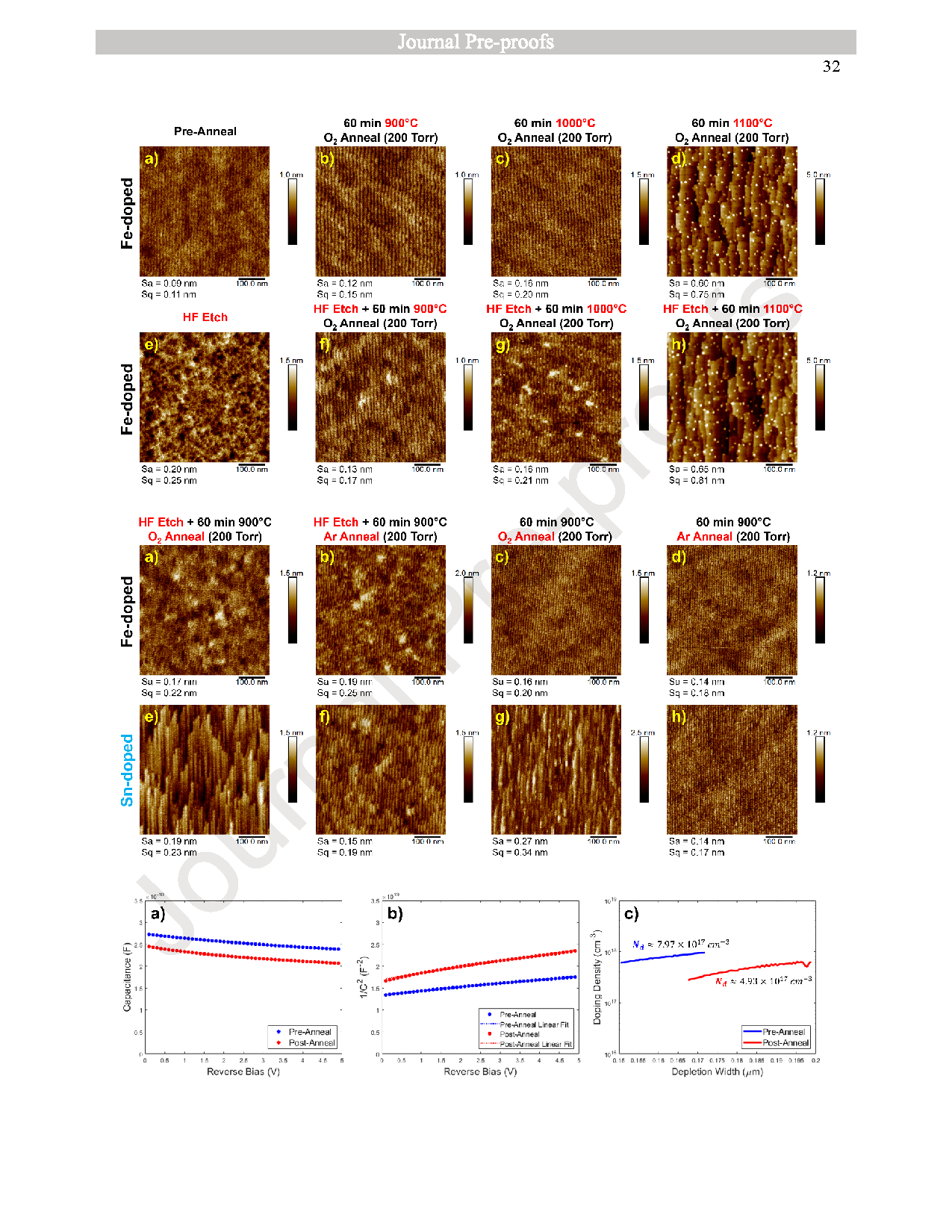
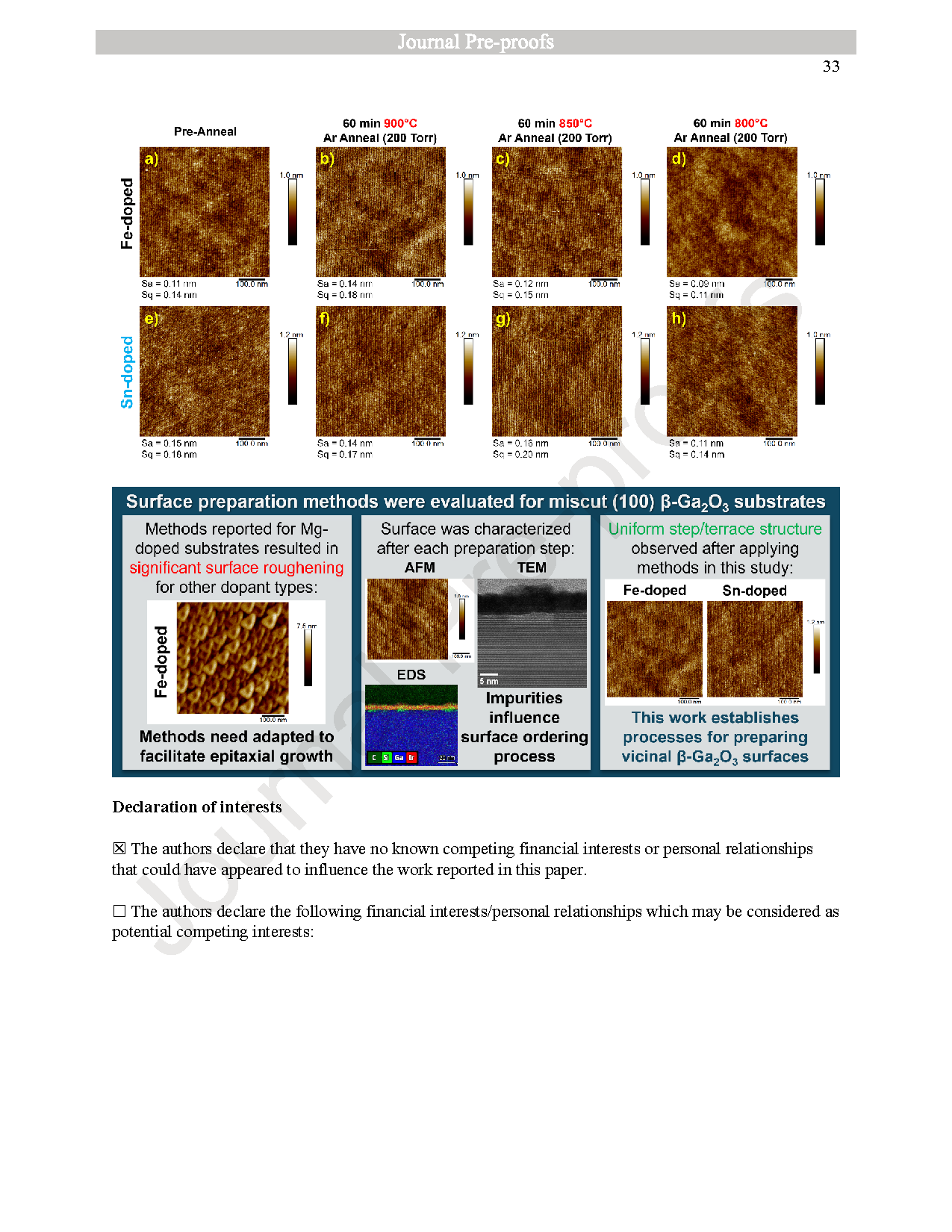
For both Fe-doped and Sn-doped, miscut (100) β-Ga₂O₃ substrates, annealing for 60 min at 850-900°C and 200 Torr resulted in uniform surface steps/terraces and an average surface roughness of <0.2 nm Sq/rms. Similar results were observed when annealing the insulating, Fe-doped substrates in O₂ and Ar atmospheres, providing flexibility to modulate the environment based on the specific epitaxial growth process and/or need to control the concentration of VGa. For the conductive, Sn-doped substrates, a well-defined step/terrace structure was also achieved while maintaining surface conductivity by keeping PO₂ sufficiently low during the annealing step. Further, while roughening of the surface was observed when etching under acidic conditions prior to annealing, a decrease in the average surface roughness (Sq/rms <0.15 nm) was observed when etching both the Fe-doped and Sn-doped substrates in TMAH. Finally, the surface preparation process established in this study used to demonstrate epitaxial growth on miscut (100) β-Ga₂O₃ substrates with a growth rate of >2 µm/hour and a low average surface roughness of ~0.6 nm Sq/rms.
Overall, this study suggests that the surface step formation and ordering mechanism for the miscut β-Ga₂O₃ substrates is influenced by the concentration of VGa and impurities that can occupy, form defect complexes, and/or diffuse via these sites. By controlling the variables that affect the formation/compensation of VGa, both insulating and conductive, miscut (100) β-Ga₂O₃ substrates can be prepared with vicinal surfaces suitable for epitaxial growth.
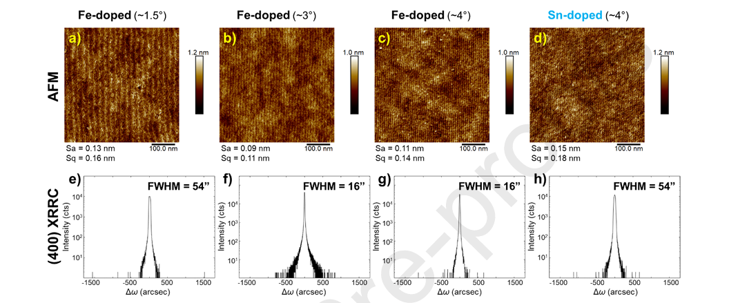
Figure 1 Summary of 500x500 nm AFM scans (a-d) and (400) XRRCs (e-h) collected for ~1.5° miscut, Fe-doped (a and e), ~3° miscut, Fe-doped (b and f), ~4° miscut, Fe-doped (c and g), and ~4° miscut, Sn-doped (d and h) (100) β-Ga₂O₃ substrates following final CMP.
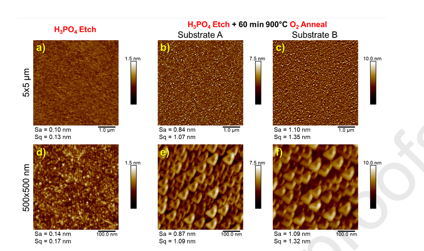
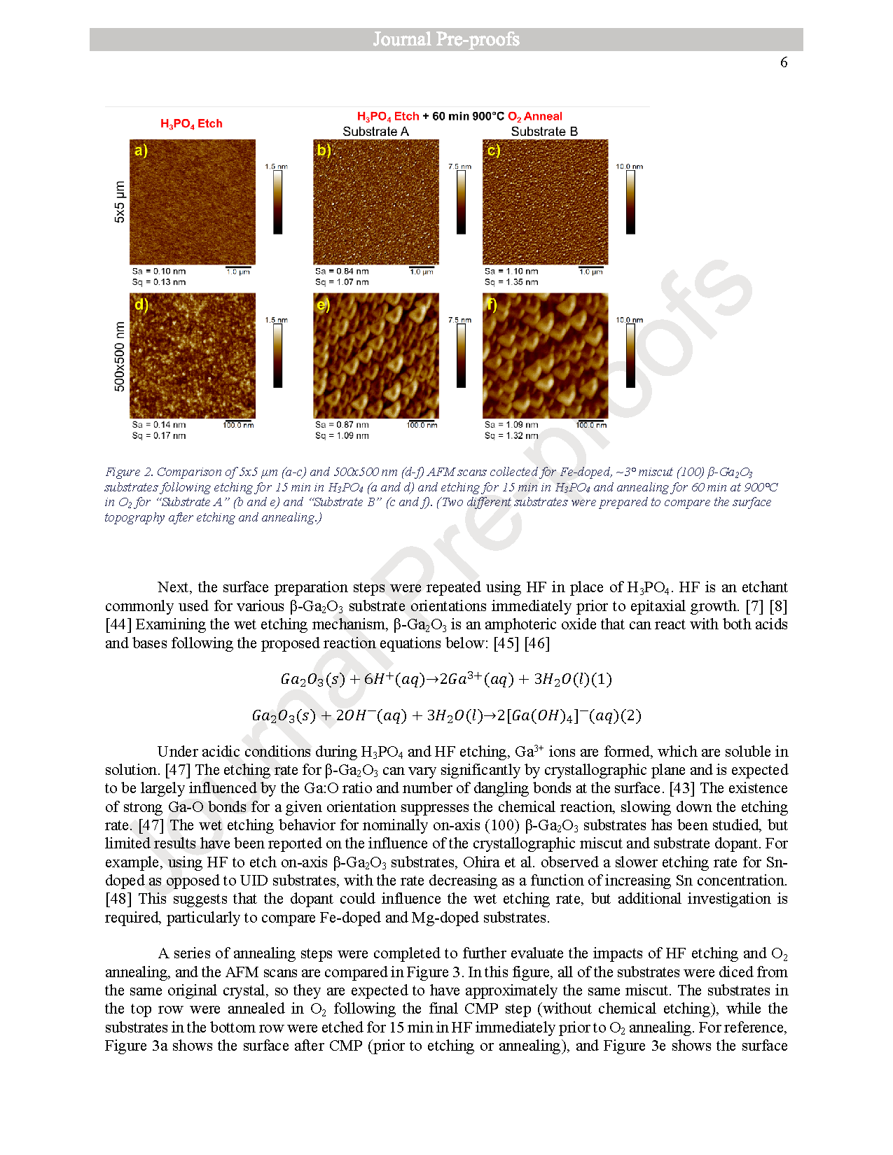
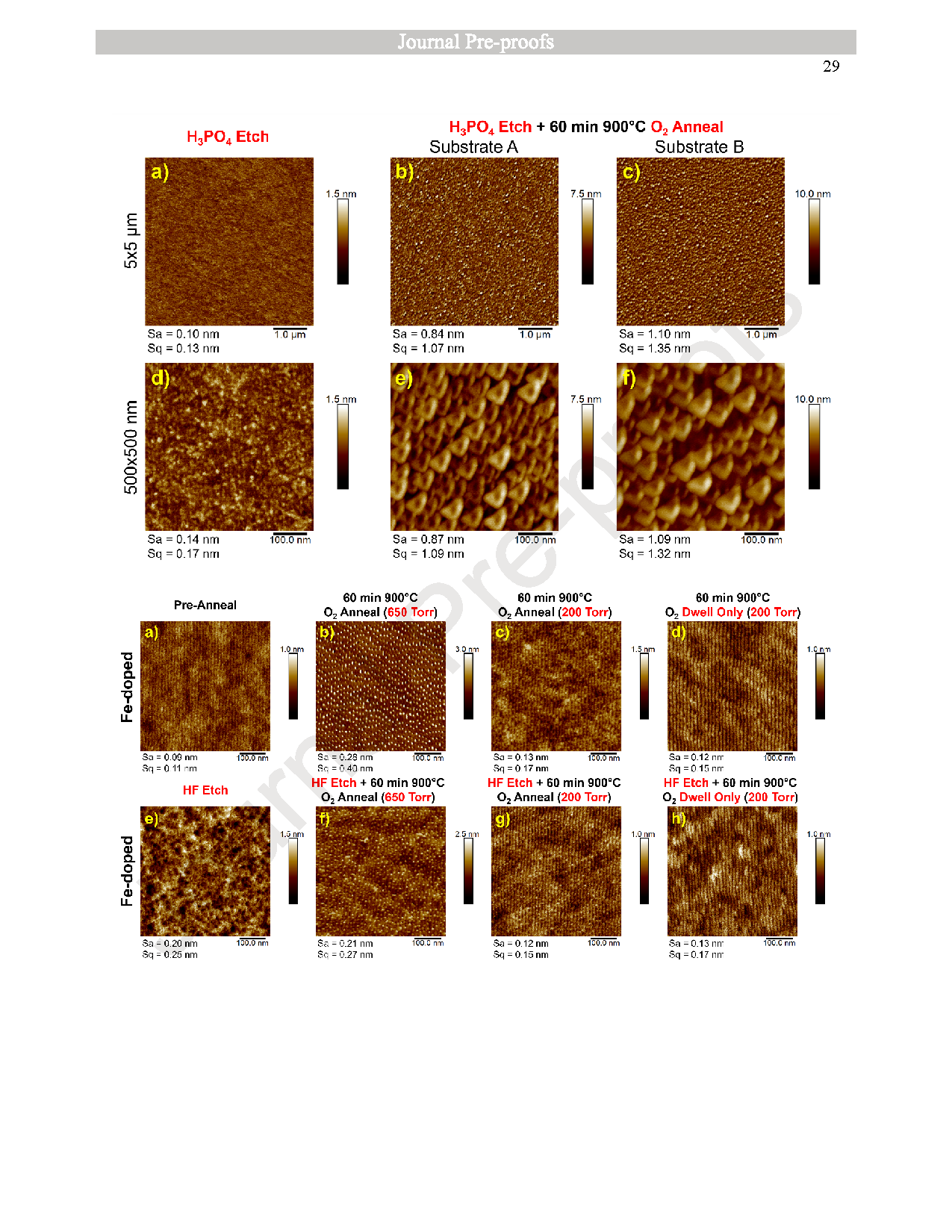
Figure 2 (a-c) 5x5 µm AFM scans and (d-f) 500x500 nm AFM scans for β-Ga₂O₃ substrates following etching for 15 min in H₃PO₄ (a and d) and etching for 15 min in H₃PO₄ and annealing for 60 min at 900°C O₂ (b and c), showing the surface topography of Substrate A and Substrate B.
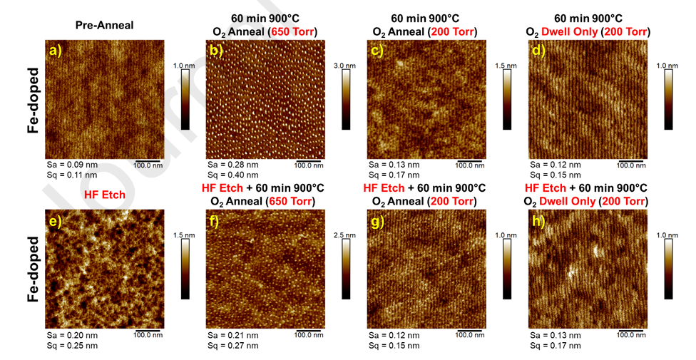
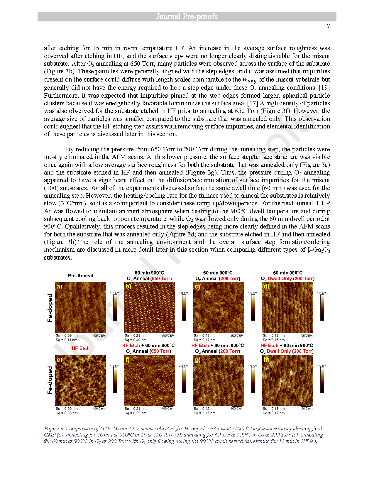
Figure 3 Comparison of 500x500 nm AFM scans collected for Fe-doped, ~3° miscut (100) β-Ga₂O₃ substrates following final CMP (a), annealing for 60 min at 900°C in O₂ at 650 Torr (b), annealing for 60 min at 900°C in O₂ at 200 Torr (c), annealing for 60 min at 900°C in O₂ at 200 Torr with O₂ only flowing during the dwell period (d), etching for 15 min in HF (e), etching for 15 min in HF and annealing for 60 min at 900°C in O₂ at 650 Torr (f), etching for 15 min in HF and annealing for 60 min at 900°C in O₂ at 200 Torr (g), etching for 15 min in HF and annealing for 60 min at 900°C in O₂ at 200 Torr with O₂ only flowing during the dwell period (h).
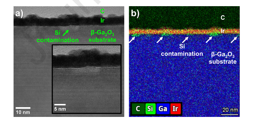
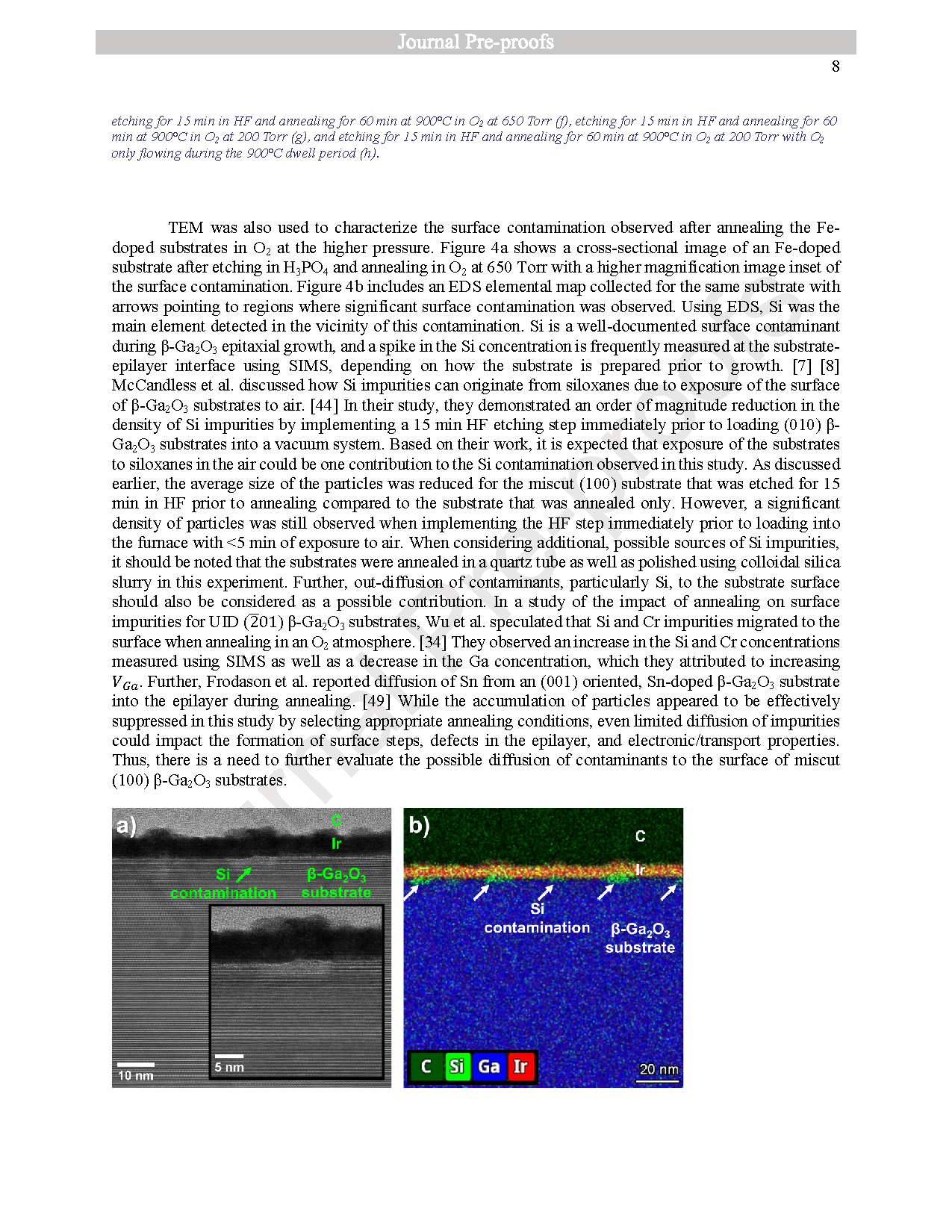
Figure 4 Cross-sectional TEM image with higher magnification image inset (a) and EDS map with arrows indicating regions with high atomic percentage of Si (b) for an Fe-doped (100) β-Ga₂O₃ substrate following etching for 15 min in H₃PO₄ and annealing for 60 min at 900°C in O₂ at 650 Torr.
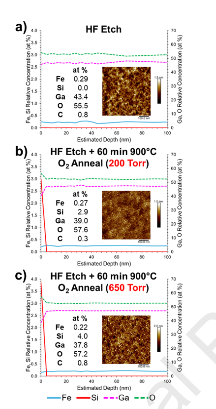
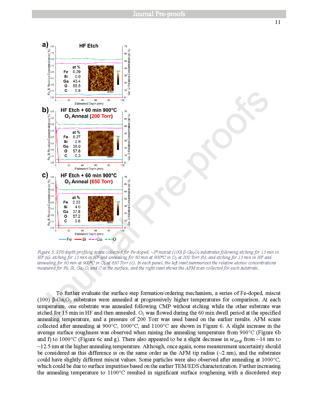
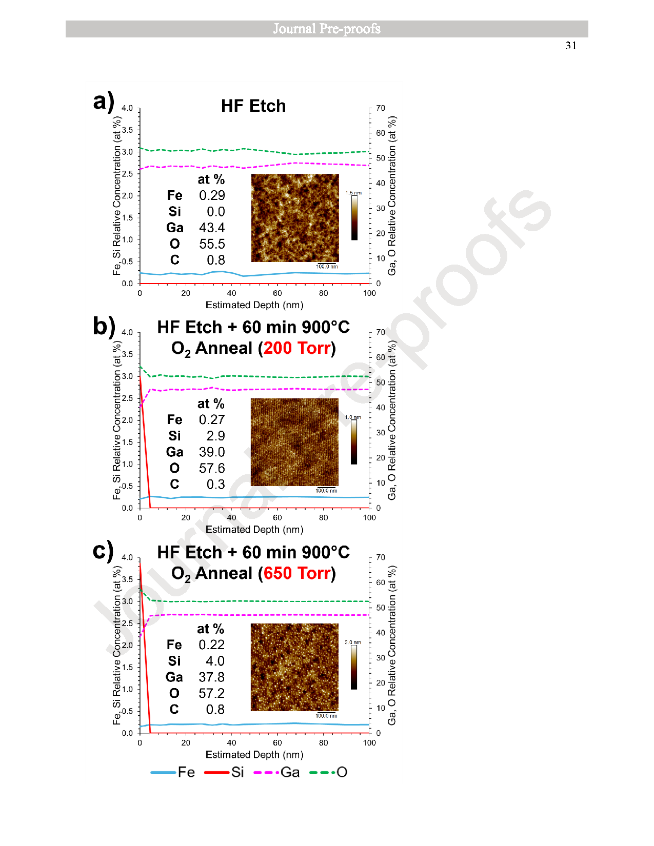
Figure 5 XPS depth profiling scans collected for Fe-doped, ~3° miscut (100) β-Ga₂O₃ substrates following etching for 15 min in HF (a), etching for 15 min and annealing for 60 min at 900°C in O₂ at 200 Torr (b), and etching for 15 min and annealing for 60 min in O₂ at 650 Torr (c). In each panel, the left inset summarizes relative atomic concentrations of Fe, Si, Ga, O, C at surface, and the right inset shows corresponding AFM scan.
DOI:
doi.org/10.1016/j.apsusc.2026.167611
Instruction
Official Account

Cooperation
Top
