


Researchers from the University of Science and Technology of China have published a paper titled "Investigation of Bias Temperature Instability in β-Ga₂O₃ UMOSFET with N-ion Implanted Current Blocking Layers" (Research on Bias Temperature Instability of β-Ga₂O₃ Trench MOSFETs with Nitrogen-Ion Implanted Current Blocking Layers) at the academic conference 2026 IEEE 38th International Symposium on Power Semiconductor Devices and ICs (ISPSD).
Abstract
We report the first comprehensive bias temperature instability characterization of vertical β-Ga₂O₃ UMOSFETs featuring nitrogen-ion-implanted current blocking layers (CBLs). The device exhibits exceptional stability under negative bias stress at - 20 V. This result effectively validates the integrity of the CBL junction, confirming the absence of mobile ions or leakage-inducing defects in the implanted region. Conversely, positive bias stress reveals a threshold voltage (VTH) instability dominated by electron trapping. Kinetic analysis yields a low time exponent (n=0.12) independent of stress voltage and a near-linear dependence on gate overdrive (γ=1.1), characteristic of tunneling into pre-existing traps. Furthermore, the invariant subthreshold swing and an extracted activation energy of EA= 0.42 eV suggests that the instability is primarily attributed to phonon-assisted tunneling into border traps, with negligible generation of slow interface states. Recovery analysis based on a universal relaxation model reveals an incomplete restoration, confirming that the permanent component stems from deep traps with extremely long emission times.
Highlights
For the first time, complete Bias Temperature Instability (BTI) reliability characterization is implemented on vertical β-Ga₂O₃UMOSFET with N-ion implanted current blocking layer, and the device stability difference under negative and positive bias stress is distinguished.
The N-implanted CBL structure shows negligible threshold voltage shift under heavy negative bias stress of -20 V, verifying perfect junction integrity without mobile ions or leakage defects.
The kinetic law of Positive Bias Temperature Instability (PBTI) is quantitatively analyzed: time exponent n=0.12 and voltage acceleration factor γ=1.1. Combined with activation energy of 0.42 eV, the dominant degradation mechanism is confirmed as phonon-assisted electron tunneling into gate dielectric border traps instead of massive generation of interface states.
Multi-dimensional tests including double pulse sweep, temperature-variable stress and relaxation recovery separate recoverable and permanent threshold shift components, proving irreversible degradation originates from deep-level traps.
This work identifies that ALD-Al₂O₃ gate dielectric defects are the primary reliability bottleneck, providing core optimization guidance for gate stack design of Ga₂O₃ power devices.
Conclusion
In this work, we presented the first comprehensive reliability assessment vertical β-Ga₂O₃ UMOSFETs featuring CBL. First, the device demonstrates exceptional robustness under NBS (- 20 V), showing negligible threshold voltage shift. Consistent with the deep depletion nature of the β-Ga₂O₃ interface, this stability confirms that the CBL preserved the junction integrity without introducing mobile ions or leakage channels. Second, the primary reliability bottleneck is identified as Positive Bias Instability caused by electron trapping. Through rigorous kinetic analysis, we observed an invariant subthreshold swing, a low time exponent (n=0.12), and a near-linear dependence on gate overdrive (γ=1.1). These signatures suggest that the degradation is governed by phonon-assisted tunneling into pre-existing border traps, rather than the generation of slow interface states detectable within the measurement window. The incomplete recovery observed even after 10⁴ s verifies the presence of deep border traps and the propagation of the electron tunneling front into the dielectric. The findings clarify that future efforts to enhance the dynamic stability of vertical Ga₂O₃ power devices should prioritize the optimization of the gate dielectric quality.
Project Support
This work is supported by the National Key Research and Development Program of China (No. 2024YFE0205200), the National Natural Science Foundation of China under Grant nos. 62404214, 62522411, U23A20358, 62234007, 62474170 and 61925110, the University of Science and Technology of China (USTC) Research Funds of the Double First-Class Initiative under Grant No. WK2100000055, the Project of 46th Research Institute of CETC under Grant no. WDZC202446007, the open research fund of Suzhou Laboratory under Grant no. SZLAB-1208-2024-ZD012.
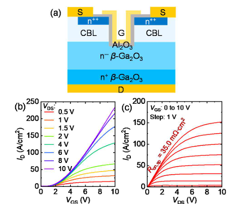
Figure 1 (a) Cross-sectional schematic of the fabricated β-Ga₂O₃ UMOSFET with N-ion implanted CBL. (b) Pulsed transfer characteristics and (c) pulsed output characteristics measured at room temperature.
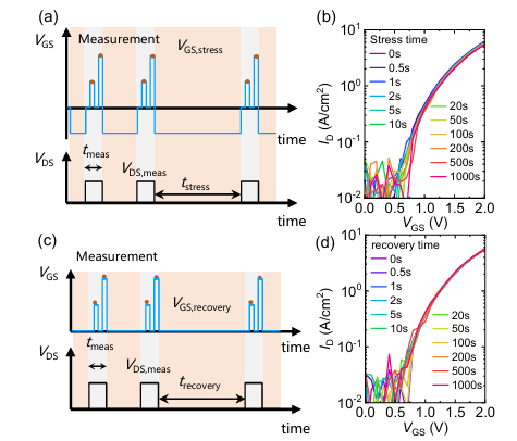
Figure 2 (a) Schematic of the NBS measurement sequence. (b) Evolution of transfer characteristics under a constant gate stress of − 20 V for stress times up to 1000 s. (c) Schematic of the recovery measurement sequence. (d) Transfer characteristics during the recovery phase. The negligible V_TH shift indicates excellent stability of the device under negative bias.
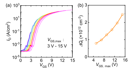
Figure 3 (a) Transfer characteristics measured with varying maximum gate sweep voltages (VGS,max) at V_DS of 10 V. (b) Extracted trapped charge density (ΔQt) versus VGS,max
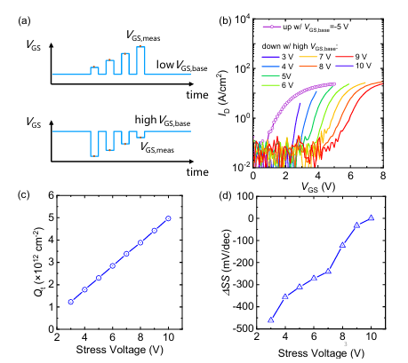
Figure 4 (a)Schematic of the double-sweep pulse-mode VGS waveforms used to characterize hysteresis. (b) Pulse-mode double-sweep transfer characteristics measured with increasing maximum gate voltage (VGS,max) from 3 V to 10 V, exhibiting significant hysteresis loops. (c) Calculated trapped charge density (ΔQt) as a function of stress voltage. (d) ΔSS observed during the hysteresis sweeps as a function of stress voltage.
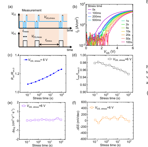
Figure 5 (a) Schematic of the Positive Bias Stress measurement sequence. (b) Evolution of transfer characteristics under a PBS of 6 V for varying stress times. Time evolution of (c) normalized on-resistance (Ron/Ron,0), (d) normalized maximum drain current (Imax/Imax,0), (e) field-effect mobility change (ΔμFE), and (f) subthreshold swing change (ΔSS).
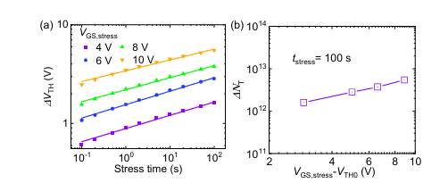
Figure 6 (a) Threshold voltage shift (ΔVTH) as a function of stress time under different gate stress voltages (VGS,stress = 4, 6, 8, 10 V), exhibiting a power-law dependence (ΔVTH ∝ tⁿ). (b) Dependence of the trapped charge density (ΔNt) on the gate overdrive voltage (VGS,stress−VTH0) at a fixed stress time of 100 s.
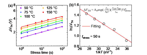
Figure 7 (a) Time evolution of ΔV_TH under PBS measured at different temperatures ranging from 50 °C to 150 °C. (b) Arrhenius plot of ln(ΔVTH) versus 1/kT at a stress time of 50 s. The linear fit indicates a thermally activated trapping process.
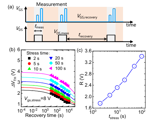
Figure 8 (a) Schematic of the recovery measurement sequence after PBS. (b) Recovery traces of ΔVTH as a function of relaxation time after applying a stress voltage of 8 V for different durations. (c) Recoverable voltage component versus stress time.
DOI:
10.1109/ISPSD64561.2026.11553773
Instruction
Official Account

Cooperation
Top
