


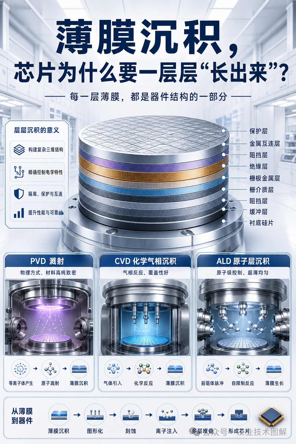
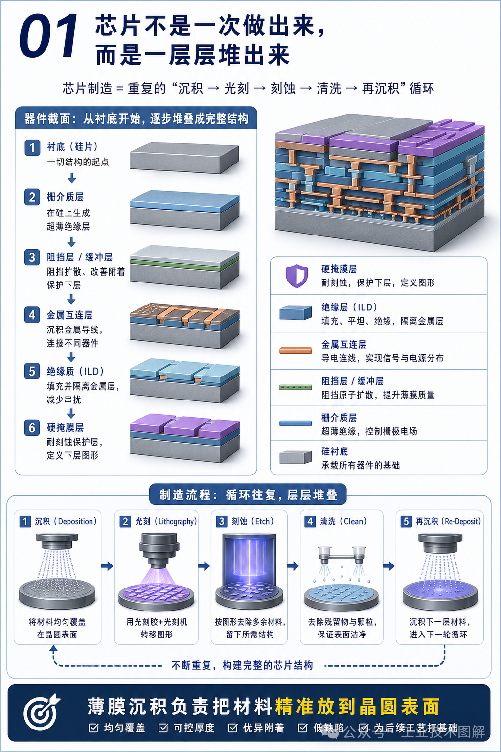
Semiconductor manufacturing is not a single step of patterning structures onto a wafer, but a repetitive process of deposition, lithography, etching, and cleaning, gradually building devices layer by layer.
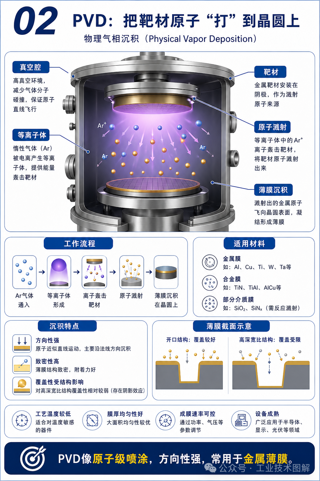
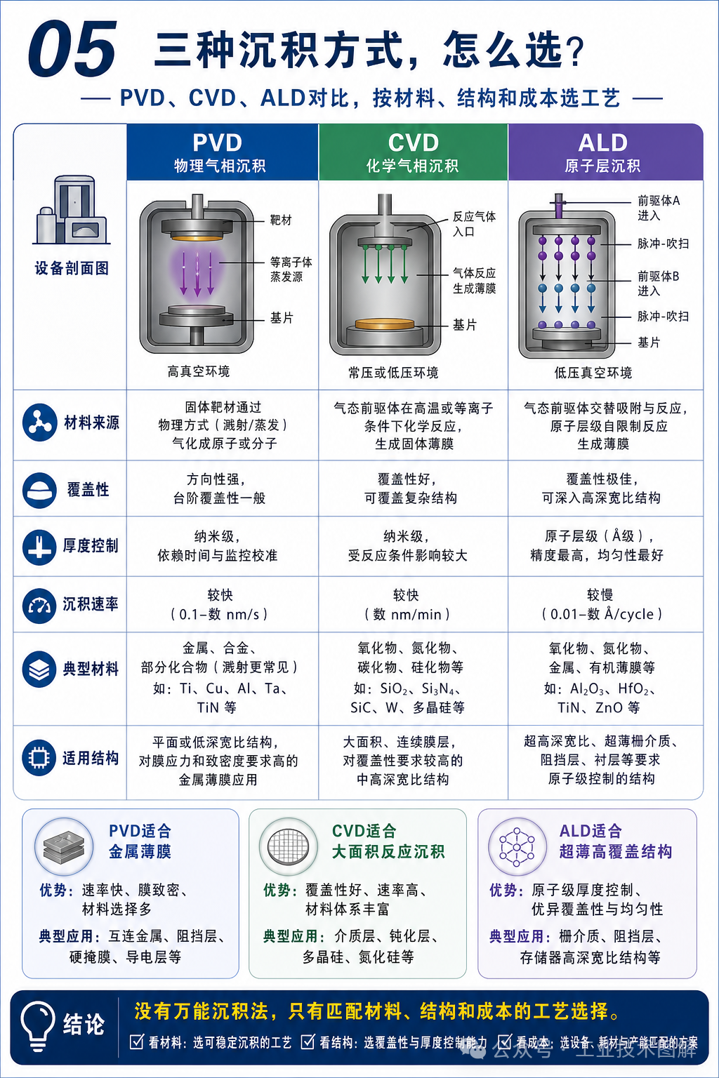
PVD (Physical Vapor Deposition) works like atomic-scale spray coating and is commonly used for metal thin films.
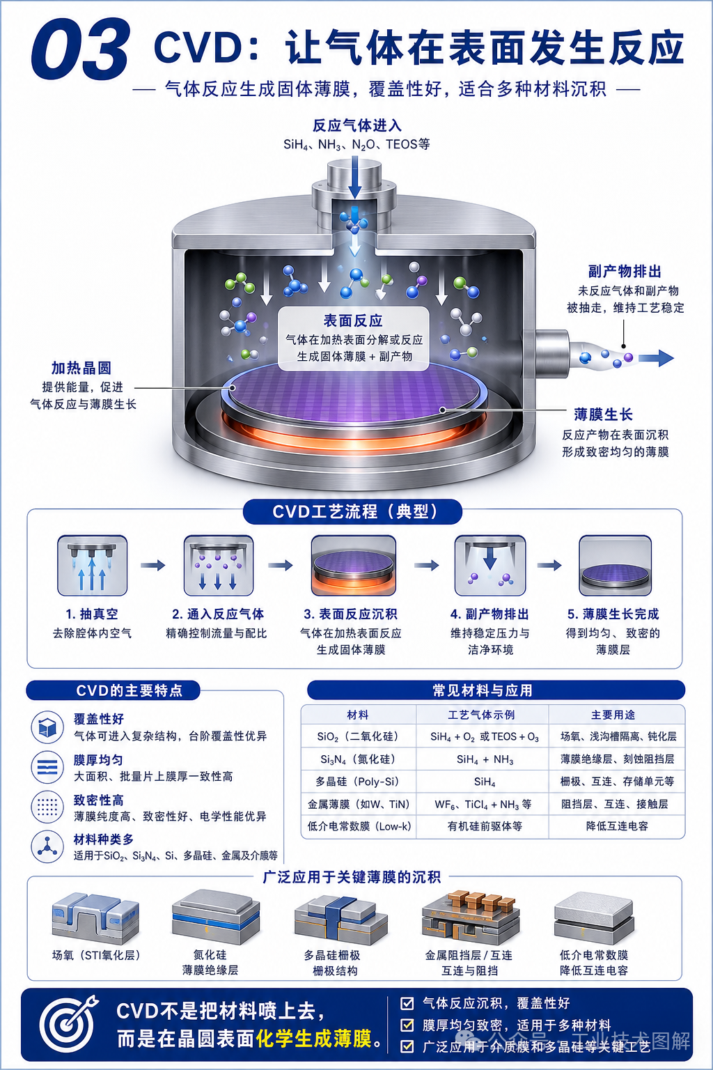
CVD (Chemical Vapor Deposition) enables gas-phase precursors to react and form solid thin films on the wafer surface.
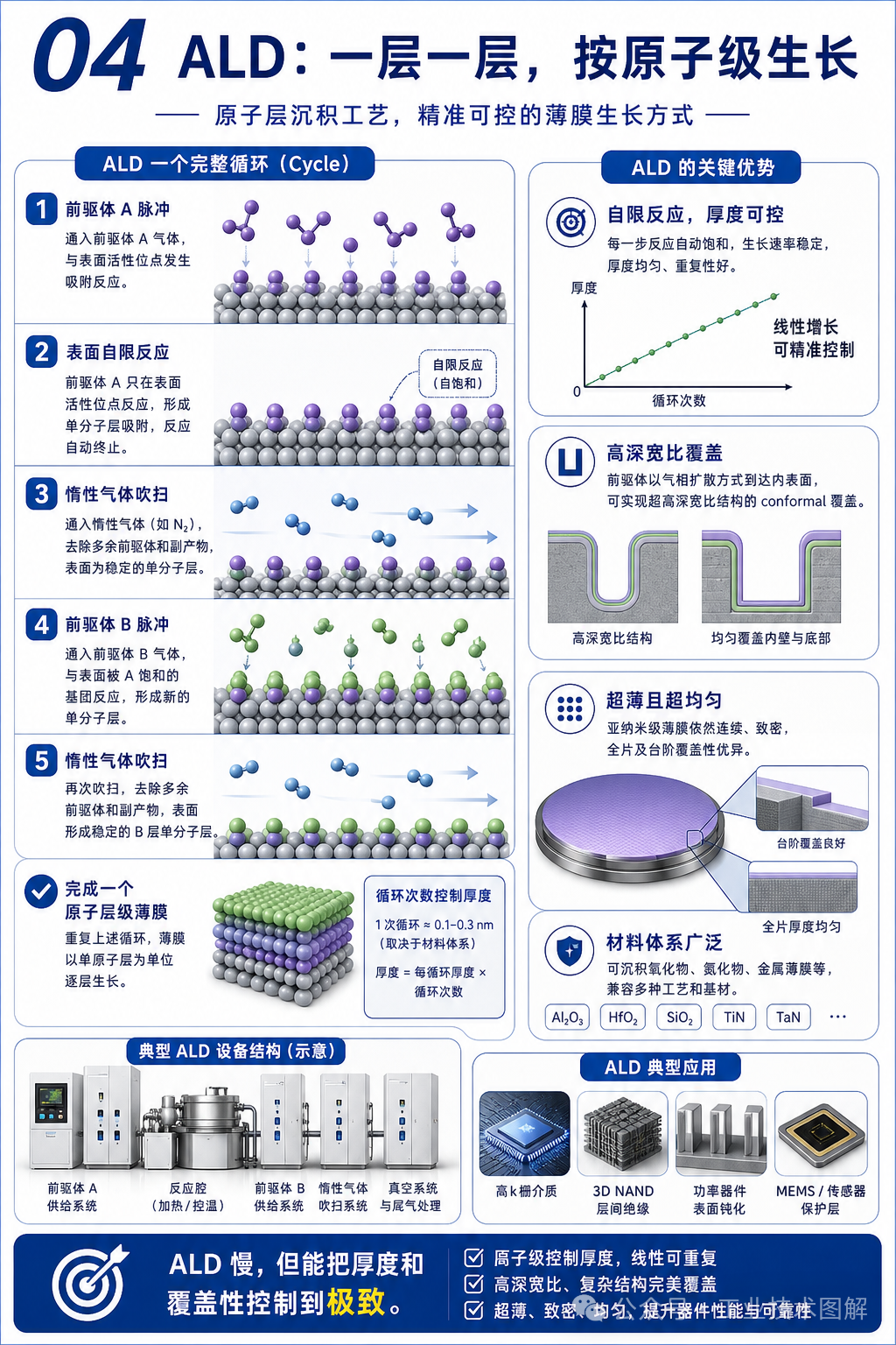
ALD (Atomic Layer Deposition) achieves atomic-scale thickness control through self-limiting surface reactions.
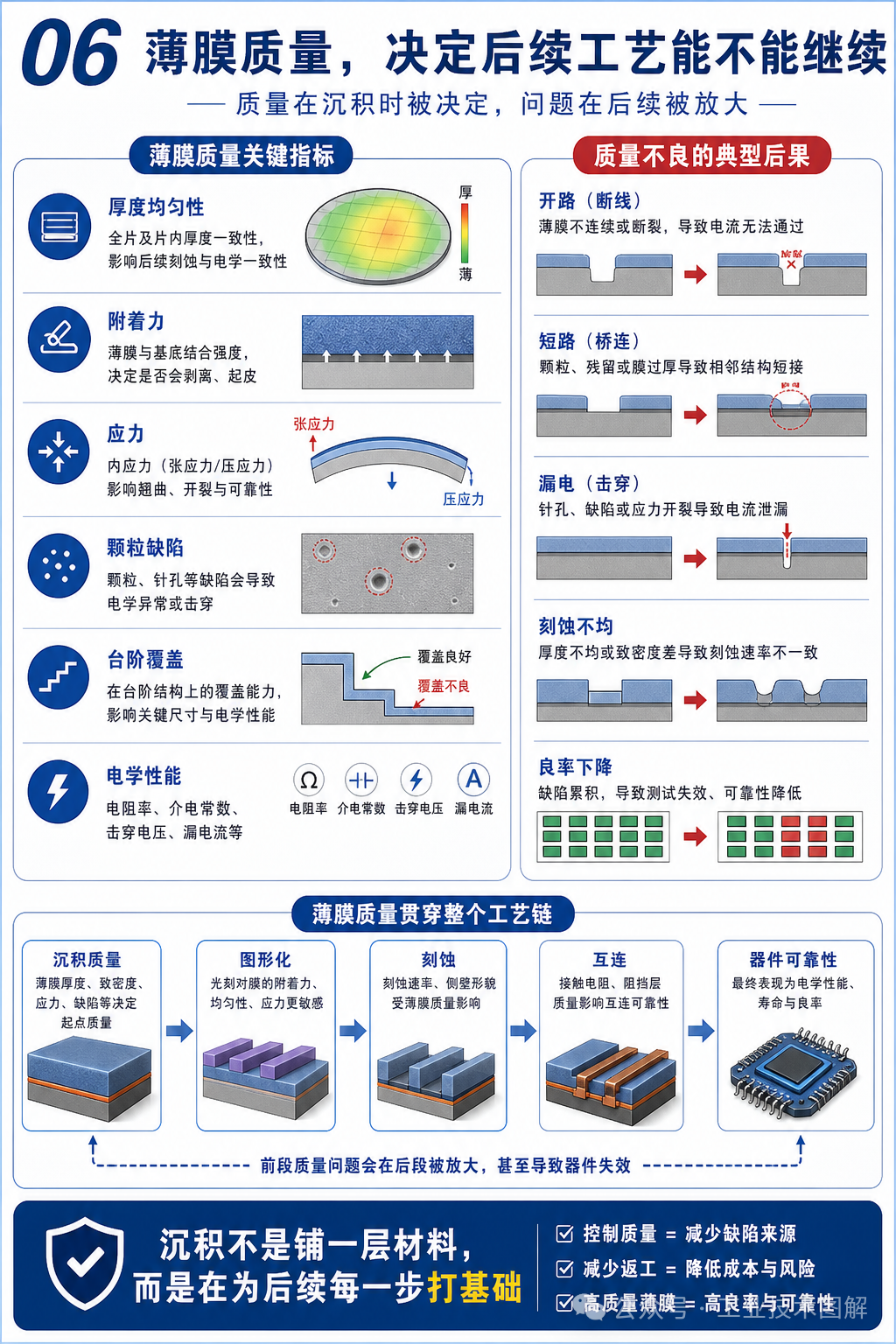
The uniformity, stress, step coverage, and defect density of thin films directly affect downstream process integration and ultimately determine device performance and chip yield.
Instruction
Official Account

Cooperation
Top
