



Comprehensive Strength of the Nano-Fabrication Platform
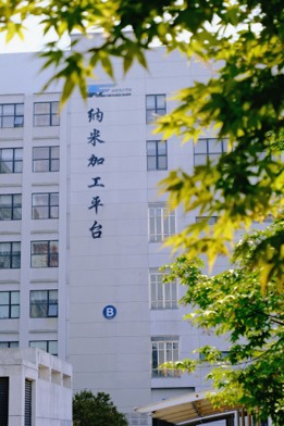
Infrastructure Capabilities
I. The Nano-Fabrication Platform is equipped with a 10,000 m² class-100/1000 cleanroom facility and more than 300 sets of major equipment. It provides strong capabilities for research and development of microelectromechanical systems (MEMS), optoelectronic devices, power devices, microfluidic systems,
II. Collaborative Innovation and R&D Ecosystem
The platform has established an integrated innovation model that brings together industry, academia, research, and testing through close collaboration with enterprises and universities.
1.Its research scope covers a wide range of advanced fields, including (ultra-)wide bandgap semiconductor materials and devices, compound semiconductors, spintronics, two-dimensional materials and devices, power and RF devices, optoelectronic devices, photonic integrated circuits, heterogeneous integration, and micro-system integration processes.
2.The platform operates 6-inch and below R&D lines, as well as 8-inch pilot-scale and small-to-medium-scale production lines, enabling rapid iteration from laboratory prototypes to engineering samples.
3.On this basis, it has established the CAS Nano-Tech Zhangjiagang Compound Semiconductor Research Institute and the Guangdong Institute of Semiconductor Micro/Nano Manufacturing Technology to provide strong support for industrialization.
Soft Strengths of the Nano-Fabrication Platform
The Nano-Fabrication Platform is supported by an internationally competitive and nationally leading high-level talent team of over 150 members, covering R&D, process engineering, equipment maintenance, and facility support. The platform has supported more than 200 major scientific and technological projects and serves over 300 research institutions annually.
Core Business of the Nano-Fabrication Platform
One-Stop Micro/Nano Fabrication and R&D Services
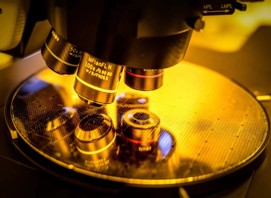
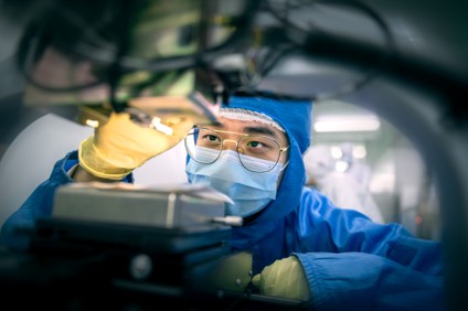
The Nano-Fabrication Platform provides integrated, full-chain services for microelectronics, optoelectronics, MEMS, biochips, and nanodevices, ranging from technical consultation and process development to contract fabrication, in-house processing, and joint technical R&D. The platform also offers professional process guidance, equipment training, and technical support, enabling users to quickly get started, accelerate project execution, and cultivate technical talent efficiently.
Its process services cover key semiconductor fabrication steps, including epitaxy, photolithography, etching, thin-film deposition, ion implantation, annealing, packaging, and metrology. These capabilities support advanced R&D of MEMS devices, optoelectronic devices, power and RF devices, magnetic devices, quantum devices, Micro-LEDs, and heterogeneous integration systems.
Two service modes are available:
Contract Fabrication (Service Mode):
Experienced engineers execute sample fabrication based on process parameters provided by the customer, significantly reducing early-stage R&D time and experimental cost for enterprises and academic research groups, while improving development efficiency.
User-Operated Fabrication (Training Mode):
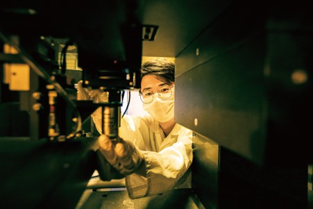
After systematic training, customers are provided with facility access and equipment, allowing authorized personnel to independently perform sample fabrication.
This model significantly reduces R&D and operational costs for startups with limited early-stage funding, while also serving as a highly cost-effective talent training platform for enterprises with technical workforce development needs.
Core Competitive Advantages and Differentiated Positioning
Compared with Pure-Play Foundries (contract manufacturing) companies, the Nano-Fabrication Platform is characterized by an open, flexible, and low-cost entry model, making it particularly suitable for exploratory “from zero to one” R&D and non-standard process validation.

Service model:
Pure-Play Foundries companies: Only accept contract fabrication; customers do not participate in the process
Nano-Fabrication Platform: Supports both contract fabrication and user-operated processing, allowing customers to participate directly in fabrication
Process flexibility:
Pure-Play Foundries companies: Fixed process menus with high customization costs
Nano-Fabrication Platform: Supports exploratory and non-standard processes, suitable for R&D-oriented projects
Sample scale:
Pure-Play Foundries companies: Mainly focused on mass production; less friendly to single-wafer or small-batch needs
Nano-Fabrication Platform: Supports single-wafer, multi-size, and small-batch processing, flexibly meeting R&D requirements
Technical communication:
Pure-Play Foundries companies: Standardized workflow with limited channels for innovation feedback
Nano-Fabrication Platform: Deep involvement of technical experts, enabling co-development of process solutions
Cost barrier:
Pure-Play Foundries companies: Relatively high barrier for startups and university research groups
Nano-Fabrication Platform: Lowered entry cost through innovation vouchers and industrial park subsidies
Typical users:
Pure-Play Foundries companies: Companies with finalized products requiring stable mass production
Nano-Fabrication Platform: Universities, research institutes, startups, and corporate R&D departments
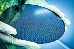
Compared with university-based R&D institutions, the Nano-Fabrication Platform offers more comprehensive equipment, more stable processes, a longer process chain, and stronger industrialization-oriented and engineering capabilities, moving beyond “single-point experiments.”

Equipment resources:
University research institutions: Dispersed equipment, often outdated models, and difficult maintenance
Nano-Fabrication Platform: Over 300 sets of major equipment, professionally managed and uniformly maintained, ensuring stable performance
Process capability:
University research institutions: Mainly single-process capabilities with limited full-flow integration
Nano-Fabrication Platform: Provides full-process coverage from epitaxy → lithography → etching → deposition → packaging → metrology
Yield and stability:
University research institutions: Highly dependent on operators, with large process variation
Nano-Fabrication Platform: Standardized process control, ensuring high stability and repeatability
Pilot-scale / small-batch capability:
University research institutions: Generally lacking pilot-line capabilities
Nano-Fabrication Platform: Equipped with an 8-inch pilot line, enabling seamless transition from R&D to manufacturing
Industrialization support:
University research institutions: Limited support, often lacking packaging, testing, and policy integration capabilities
Nano-Fabrication Platform: Supports joint R&D, industrial incubation, and policy application assistance
Openness:
University research institutions: Mostly internal-use oriented, with limited external service capacity
Nano-Fabrication Platform: Fully open to external users, accepting nationwide fabrication requests and on-site processing collaborations
Special Equipment Configuration for Gallium Oxide Process R&D
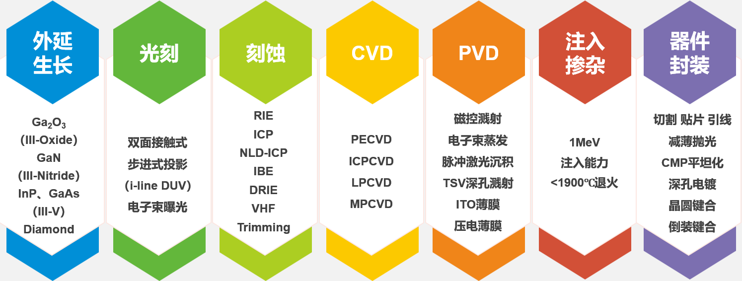
The platform is equipped with a full-process capability for epitaxial growth, device fabrication, and packaging of semiconductor materials such as gallium oxide. It supports the research and development of devices and integrated chips across (ultra-)wide bandgap power and RF electronics, semiconductor optoelectronics (light-emitting and photodetectors), MEMS, heterogeneous integration systems, and biochips.
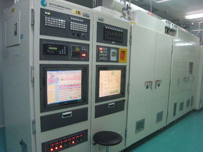
Epitaxy Equipment: TNSC MOCVD #1-Oxide
Equipment Principle
The system uses organometallic compounds of Group III elements and oxygen-based precursors as source materials. Through thermal decomposition reactions, vapor-phase epitaxial growth is carried out on substrates to form single-crystal thin films of III-oxide semiconductors and related multicomponent solid solutions.
Equipment Highlights
The MOCVD heating system has undergone specialized upgrades, significantly extending heater lifetime while enabling stable high-temperature zone control (≤1100°C). It supports high-quality epitaxial growth of Ga₂O₃ and In₂O₃ thin films on 4-inch and smaller substrates.
Main Applications
Primarily used for epitaxial growth of Ga₂O₃ thin films, In₂O₃ thin films, and Ga₂O₃ micro/nanostructures.
Technical Specifications
Temperature: up to 1100°C
Pressure: 10 kPa – 101 kPa
Rotation speed: 30 rpm
MO sources: TMGa, TEGa, TMAl, TMIn
Gases: O₂, N₂O, SiH₄
Reactor type: horizontal configuration
Sample capacity: 3 × 2-inch wafers, or 1 × 4-inch wafer
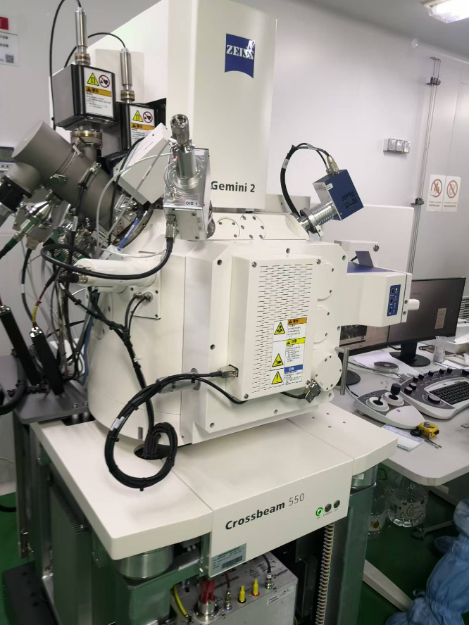
Testing Equipment: FIB ZEISS Crossbeam 550L
Equipment Principle
This system integrates high-resolution field emission scanning electron microscopy (FE-SEM) imaging and analysis with focused ion beam (FIB) machining capabilities. The gallium ion source generates an ion beam that is accelerated and focused onto the sample surface. Combined with an electron beam, it enables micro- and nanoscale defect repair, precision milling/cutting, and TEM sample preparation.
Equipment Highlights
Equipped with a large sample chamber, enabling processing and characterization of up to 8-inch wafers.
High-precision control of milling position, with real-time SEM imaging during processing for in-situ monitoring.
Main Applications
Primarily used for morphological observation, defect inspection, localization, and repair of semiconductor integrated circuits, discrete devices, and MEMS wafers/chips. It also supports cross-sectional preparation, TEM sample preparation, circuit editing/repair, and 3D reconstruction of material structures.
Technical Specifications
Electron beam column: ZEISS high-resolution GeminiSEM column
Ion source: liquid gallium ion source
Gas injection system: Pt, SiO₂
Ion beam resolution: 3 nm @ 30 kV
Maximum ion beam current: 100 nA
Sample size: up to 8-inch wafers, compatible with smaller samples
Talent Recruitment Needs of the Platform
Job Requirements
Background in semiconductors, physics, materials science, microelectronics, or related disciplines, with solid fundamental knowledge, strong English reading and writing skills, and excellent scientific research literacy, innovation ability, and teamwork spirit.
Under 35 years old, holding a PhD degree from a well-known domestic or international university or research institute.
Prior experience in semiconductors or micro/nano fabrication is preferred.
Compensation and Benefits
Base salary:
During the postdoctoral period, the annual base salary starts from RMB 280,000, and up to RMB 580,000 for outstanding candidates, plus performance-based bonuses.
Additional personal subsidies (competitive funding opportunities):
a) Jiangsu Province Outstanding Postdoctoral Program: RMB 500,000 / 300,000 / 200,000 talent allowance
b) National Postdoctoral Innovative Talent Support Program: RMB 200,000 living allowance
c) CAS Special Research Assistant Program or Institute “Excellent Postdoctoral Program”: RMB 120,000 talent allowance
d) China Postdoctoral Science Foundation General/Distinguished Funding (project funding: RMB 80,000–180,000), with additional subsidies of RMB 20,000 and RMB 50,000 respectively
Application Method
Applicants should send their CV (file name formatted as “Position–Name”) and a brief introduction via email to: xdzhang2007@sinano.ac.cn.
Shortlisted candidates will be contacted via email or phone for interview arrangements.
Instruction
Official Account

Cooperation
Top
