


The research team led by Researcher Teng Ma from the China Electronic Product Reliability and Environmental Testing Research Institute recently published an article in Applied Physics Letters entitled “Two-regime degradation associated with carrier compensation and structural instability in NiO/β-Ga2O3 heterojunction diodes under 1864 MeV Ta-ion irradiation”. The Chinese title of the article is “1864 MeV Ta离子辐照NiO/β-Ga2O3异质结二极管的两阶段退化机制研究——从载流子补偿到结构损伤”.
Background
As a representative ultrawide-bandgap semiconductor, β-Ga2O3 has a bandgap of approximately 4.8 eV and a high critical electric field, making it a promising candidate for next-generation high-voltage power devices. NiO/β-Ga2O3 heterojunction diodes, formed by integrating p-type NiO with n-type β-Ga2O3, can achieve low reverse leakage current and high blocking capability, showing potential for high-reliability power electronic systems. However, in space radiation environments, energetic heavy ions can generate defects, defect clusters, and latent tracks inside the device, leading to carrier compensation, leakage increase, forward conduction degradation, and even device failure. Previous studies have mainly focused on β-Ga2O3 Schottky devices or heterojunction devices under a single irradiation fluence, while a systematic understanding of the full degradation process of NiO/β-Ga2O3 heterojunction diodes over a wide fluence range, from electrical degradation to structural-damage-associated failure, remains insufficient.
Abstract
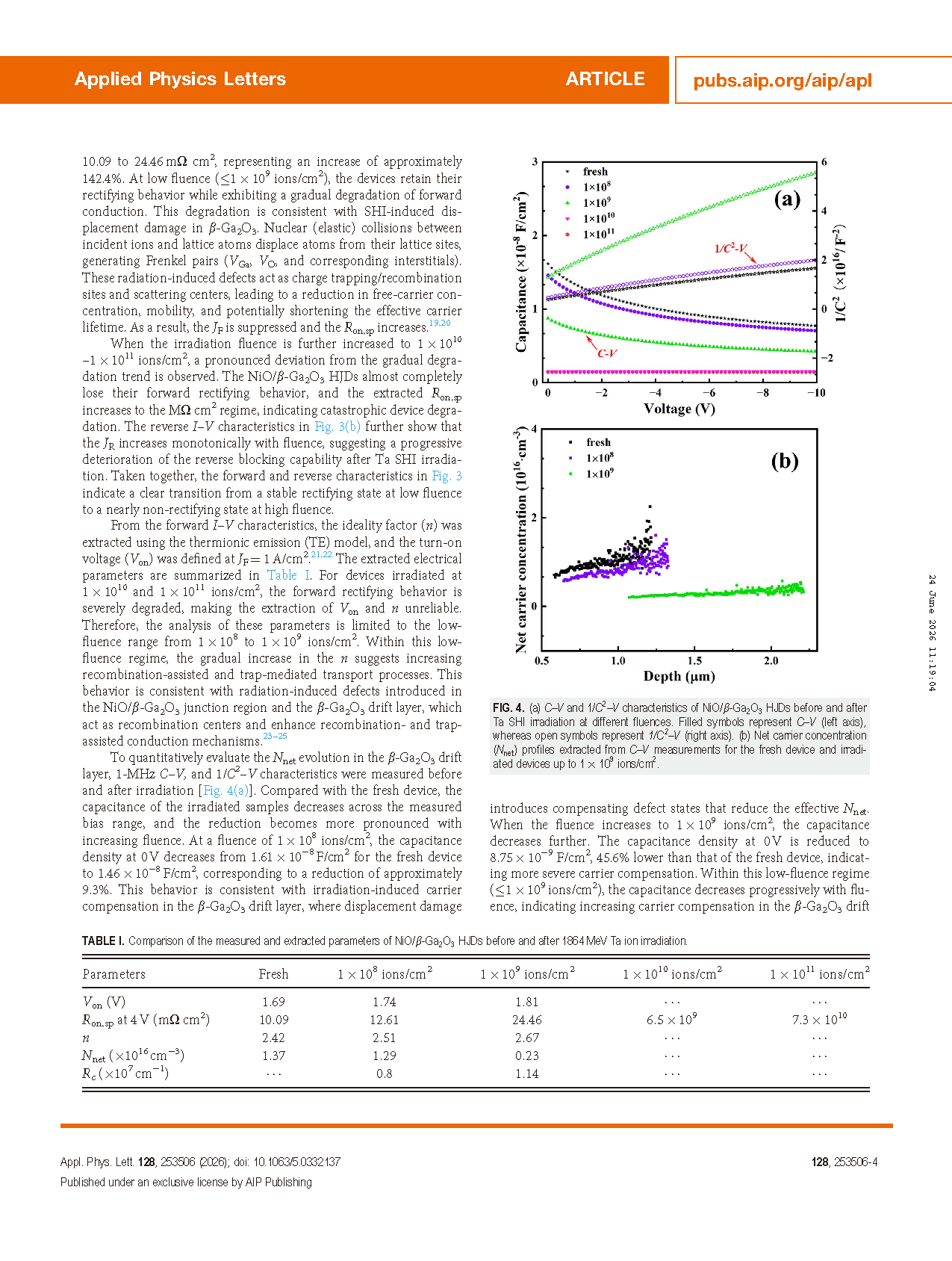
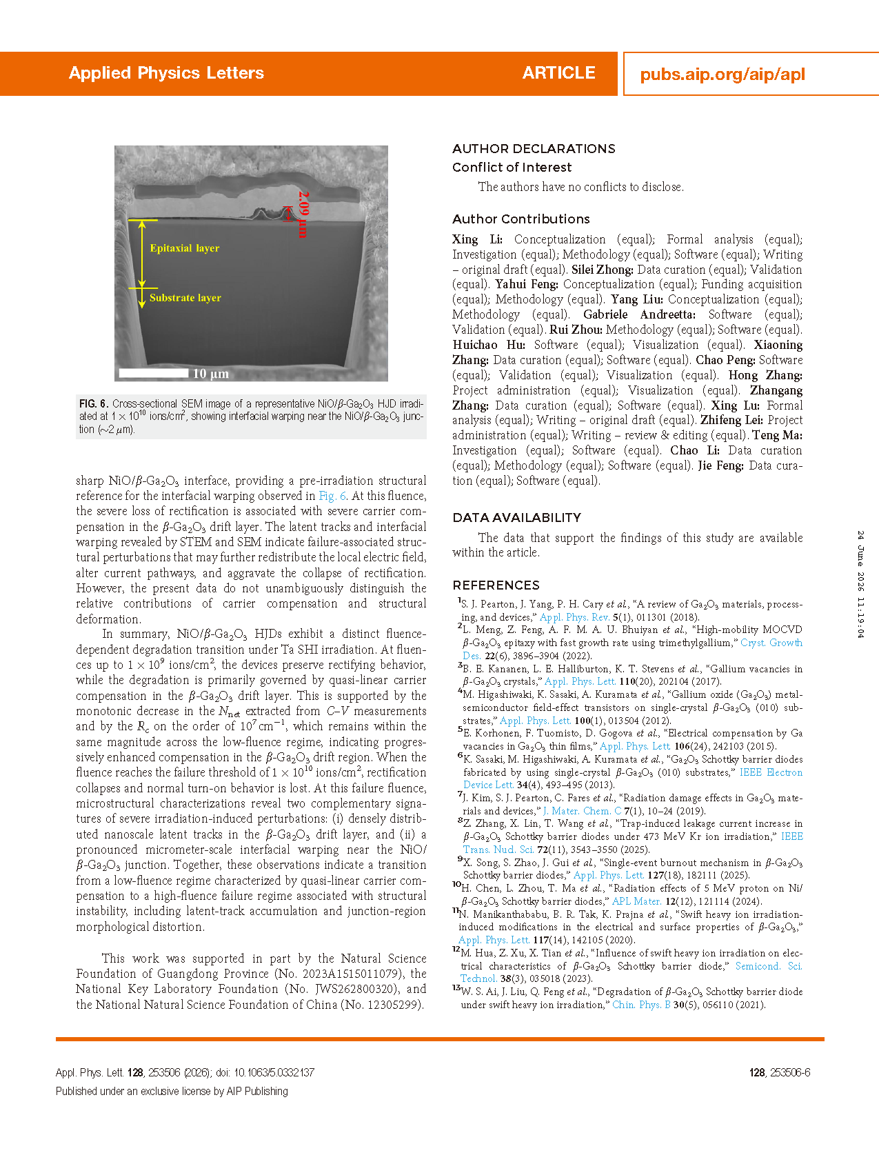
This study systematically investigates the fluence-dependent degradation behavior of NiO/β-Ga2O3 heterojunction diodes under 1864 MeV Ta-ion irradiation. The devices were irradiated over a fluence range from 1 × 10⁸ to 1 × 10¹¹ ions/cm², and their electrical and structural evolution was analyzed using I–V, C–V, STEM, and SEM characterizations. The results show that in the low-fluence regime, the devices retain rectifying behavior, while the forward current density decreases, the specific on-resistance increases, and the reverse leakage current rises. C–V analysis further reveals a reduction in the net carrier concentration of the β-Ga2O3 drift layer with increasing fluence, indicating that degradation is mainly dominated by carrier compensation. When the fluence increases to approximately 1 × 10¹⁰ ions/cm², the rectifying behavior collapses and normal turn-on behavior is lost. Structural characterization further reveals high-density nanoscale latent tracks in the β-Ga2O3 drift layer and an interfacial warping of about 2 μm near the NiO/β-Ga2O3 junction. These results demonstrate a two-regime degradation mechanism in NiO/β-Ga2O3 heterojunction diodes under heavy-ion irradiation, evolving from low-fluence carrier compensation to high-fluence structural-damage-associated failure.
Highlights
The fluence-dependent degradation behavior of NiO/β-Ga2O3heterojunction diodes under 1864 MeV Ta-ion irradiation was systematically revealed.
A two-regime degradation mechanism was proposed, evolving from low-fluence carrier compensation to high-fluence failure associated with structural damage.
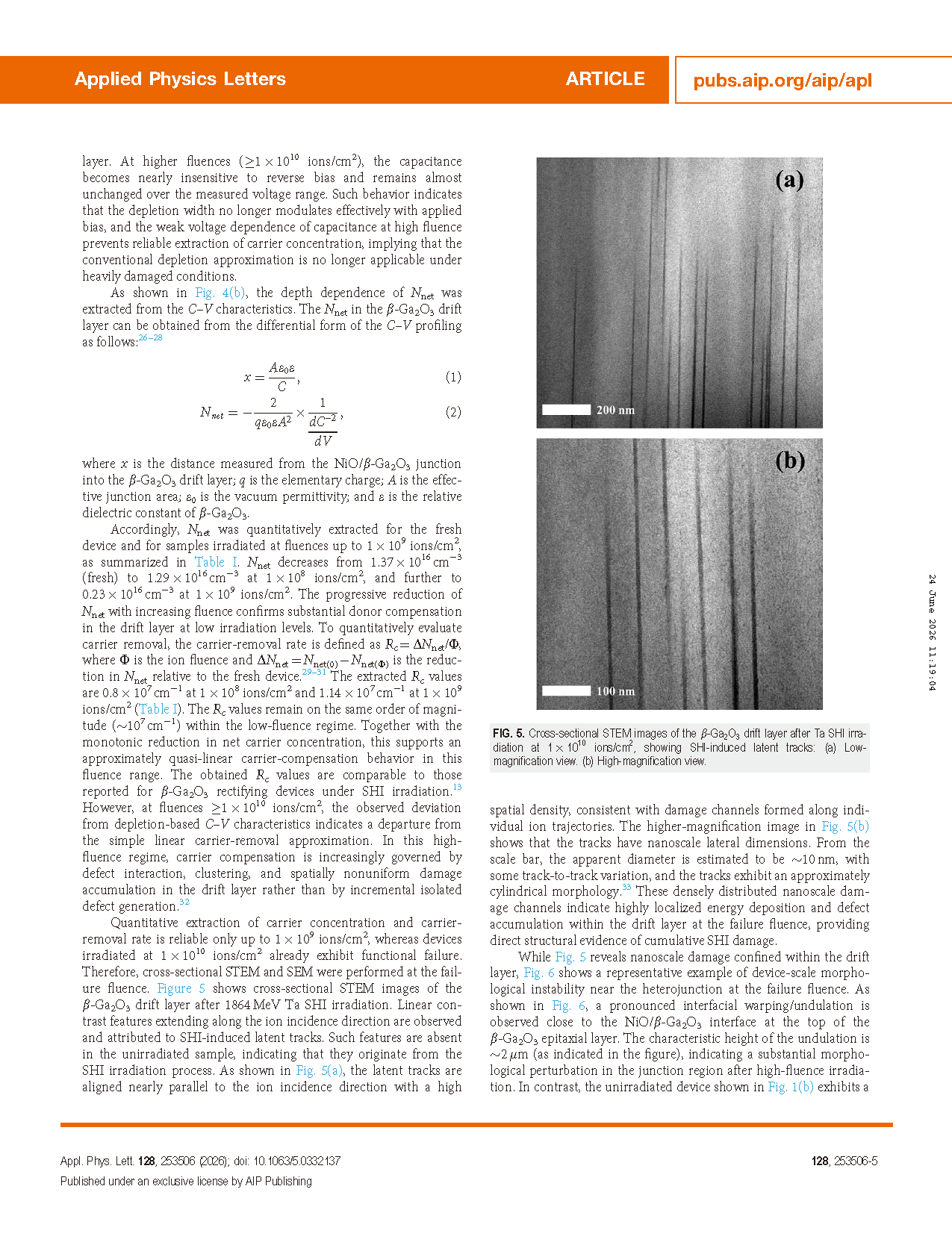
C–Vmeasurements were used to quantitatively extract the variation in net carrier concentration in the β-Ga2O3drift layer, confirming that low-fluence degradation is mainly dominated by carrier compensation.
By combining STEM and SEM characterizations, nanoscale latent tracks in the β-Ga2O3drift layer and interfacial warping near the NiO/β-Ga2O3junction were observed at high fluence.
The correlation among electrical degradation, carrier compensation, latent-track accumulation, and structural damage under heavy-ion irradiation was established, providing a reference for radiation-reliability evaluation of β-Ga2O3 heterojunction power devices.
Conclusion
This work demonstrates that NiO/β-Ga2O3 heterojunction diodes exhibit a clear two-regime degradation behavior under 1864 MeV Ta-ion irradiation. In the low-fluence regime, the devices retain rectifying behavior, and the degradation is mainly governed by carrier compensation in the β-Ga2O3 drift layer, as reflected by the reduction in net carrier concentration, degraded forward conduction, and increased on-resistance. When the fluence increases to approximately 1 × 10¹⁰ ions/cm², the rectification collapses, accompanied by high-density nanoscale latent tracks in the β-Ga2O3 drift layer and an interfacial warping of about 2 μm near the NiO/β-Ga2O3 junction. This study reveals the degradation mechanism of NiO/β-Ga2O3 heterojunction diodes from carrier compensation to structural-damage-associated failure under heavy-ion irradiation, providing an important reference for reliability evaluation and radiation-hardened design of β-Ga2O3 power devices in space radiation environments.
Project Support
This work was supported by the Natural Science Foundation of Guangdong Province (No. 2023A1515011079), the National Key Laboratory Foundation (No. JWS262800320), and the National Natural Science Foundation of China (No. 12305299).
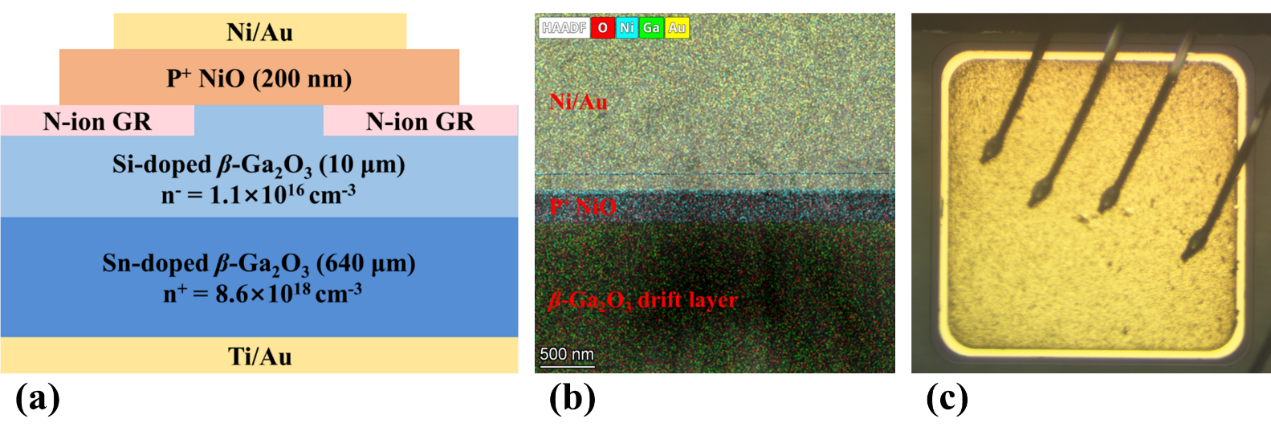
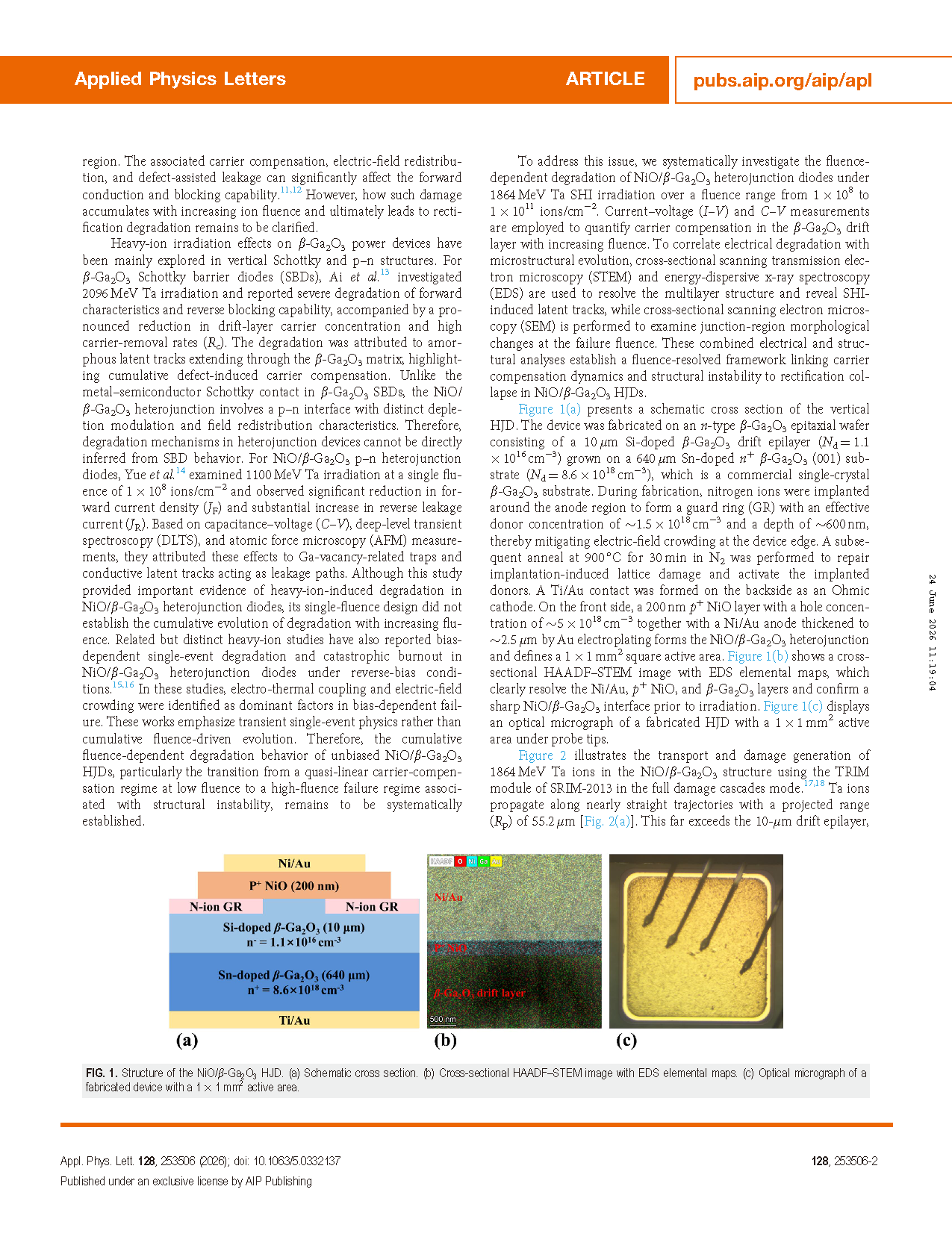
Fig. 1. Structure of the NiO/β-Ga2O3 HJD. (a) Schematic cross-section. (b) Cross-sectional HAADF–STEM image with EDS elemental maps. (c) Optical micrograph of a fabricated device with a 1 × 1 mm2 active area.
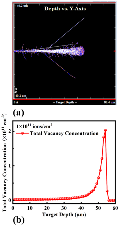
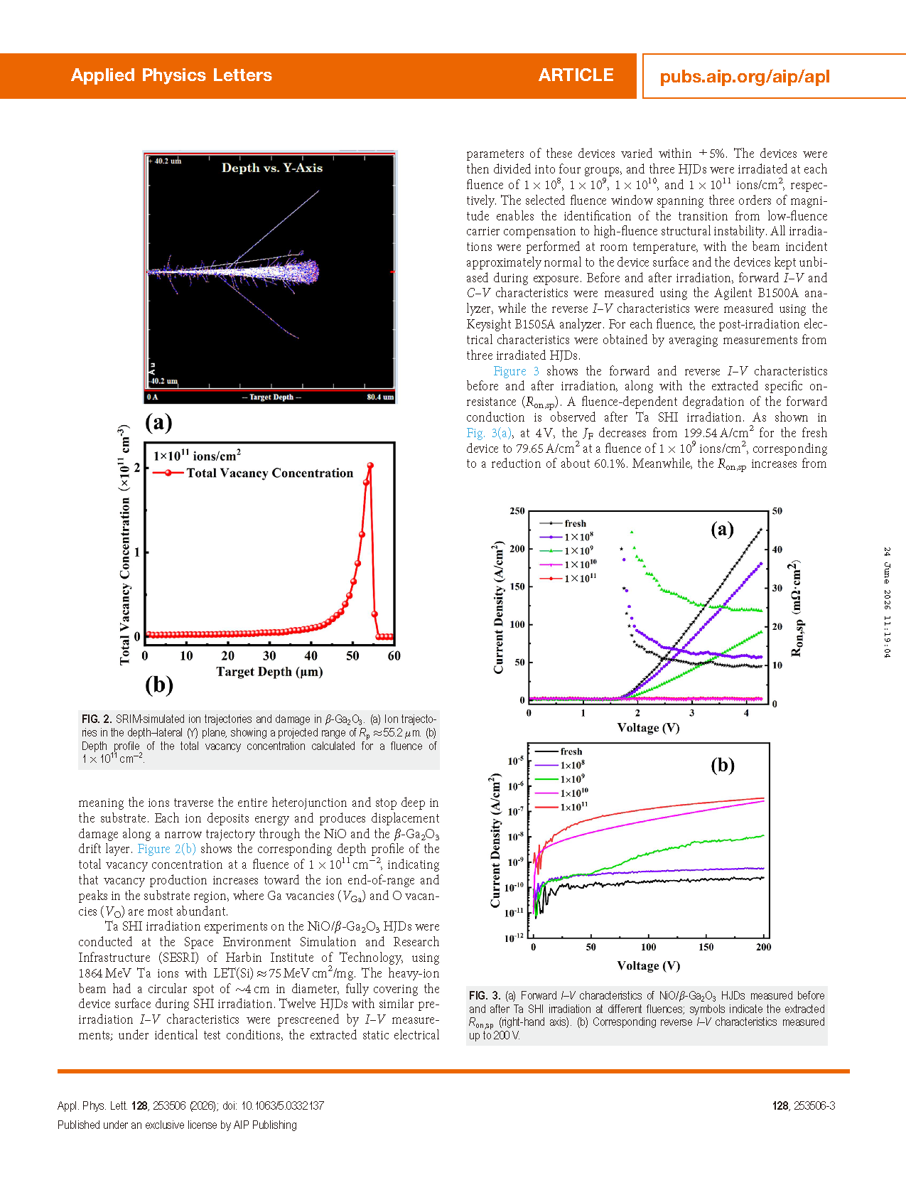
Fig. 2. SRIM-simulated ion trajectories and damage in β-Ga2O3. (a) Ion trajectories in the depth–lateral (Y) plane, showing a projected range of Rp≈55.2 μm. (b) Depth profile of the total vacancy concentration calculated for a fluence of 1×1011 cm−2.
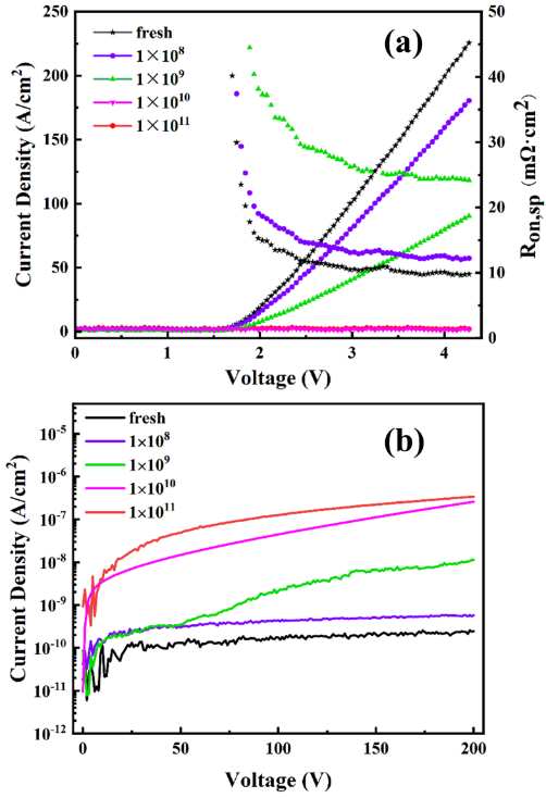
Fig. 3. (a) Forward I-V characteristics of NiO/β-Ga2O3 HJDs measured before and after Ta SHI irradiation at different fluences; symbols indicate the extracted Ron,sp (right-hand axis). (b) Corresponding reverse I-V characteristics measured up to 200 V.
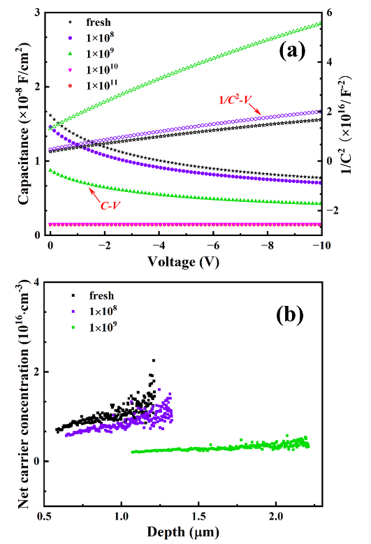
Fig. 4. (a) C–V and 1/C2–V characteristics of NiO/β-Ga2O3 HJDs before and after Ta SHI irradiation at different fluences. Filled symbols represent C–V (left axis), whereas open symbols represent 1/C²–V (right axis). (b) Net carrier concentration (Nnet) profiles extracted from C–V measurements for the fresh device and irradiated devices up to 1×10⁹ ions/cm2.
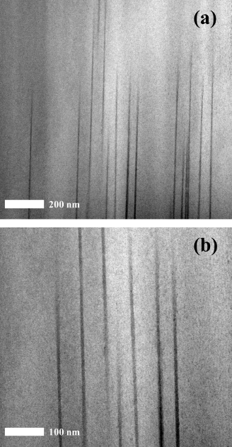
Fig. 5. Cross-sectional STEM images of the β-Ga2O3 drift layer after Ta SHI irradiation at 1×10¹⁰ ions/cm2, showing SHI-induced latent tracks: (a) Low-magnification view. (b) High-magnification view.
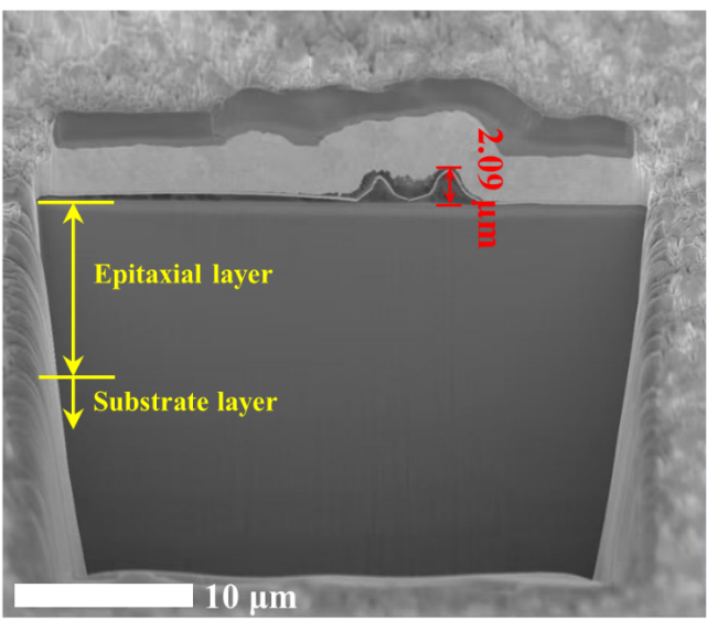
Fig. 6. Cross-sectional SEM image of a representative NiO/β-Ga2O3 HJD irradiated at 1×10¹⁰ ions/cm2, showing interfacial warping near the NiO/β-Ga2O3 junction (~2 µm).
DOI:
doi.org/10.1063/5.0332137
Instruction
Official Account

Cooperation
Top
