


Introduction:
Whether a substrate can truly be used for device fabrication depends not only on its size, nor simply on whether its surface appears smooth and mirror-like. Defects hidden within the crystal and in the processed surface layers can have a significant impact on subsequent epitaxial quality and device reliability.
In β-Ga₂O₃ single crystals, point defects, dislocations, line defects, nanopipes, and processing-induced damage may originate either during crystal growth or during wafer slicing, grinding, and polishing processes. Some of these are merely localized material imperfections, while others may extend through the substrate, forming conductive pathways that ultimately lead to increased leakage current, reduced breakdown voltage, or fluctuations in device reliability.
In this issue, we will focus on these typical defect types and discuss the origins of defects in gallium oxide substrates, their characterization methods, and their impacts on epitaxial growth and device performance.
Issue 7:
The Invisible “Hidden Risks” — How Defects in Gallium Oxide Substrates Affect Device Performance?
Why We Need to Pay Attention to Defects in Gallium Oxide Substrates
Defects are not merely “imperfections” in material characterization. For power devices, they may act as leakage current paths, localized electric field concentration regions, or even the origin of epitaxial defects. For optoelectronic devices such as ultraviolet photodetectors, defects can introduce trap states that degrade dark current, response speed, and long-term stability.
In vertical power devices, current flows through both the epitaxial layer and the substrate. If through-type defects exist in the substrate, or if defects propagate during epitaxial growth, they may directly impact reverse leakage current, breakdown voltage, and device reliability. Therefore, understanding the types, origins, and impacts of defects in gallium oxide substrates is essential for advancing its industrial applications.
At present, commonly used techniques for characterizing defects in β-Ga₂O₃ crystals include etch pit density (EPD) statistics, X-ray topography (XRT), transmission electron microscopy (TEM), polarized optical microscopy, and atomic force microscopy (AFM). Among them, etch pit density (EPD) is one of the most widely used indicators for evaluating crystal defect density. Depending on growth methods, crystal orientations, and etching conditions, reported EPD values for β-Ga₂O₃ can vary significantly, typically ranging from 10³ to 10⁵ cm⁻² according to literature reports [1].
Main Types of Defects in Gallium Oxide Substrates
Point Defects: Microscopic Defects Affecting Stability
Point defects occur at the atomic scale and include oxygen vacancies, gallium vacancies, interstitial atoms, antisite defects, and impurity atoms. Unlike etch pits or line defects, point defects usually do not manifest as obvious morphological features under microscopy, making them difficult to identify directly through conventional surface observation.
For β-Ga₂O₃ substrates, the impact of point defects is mainly reflected in their electrical properties. On one hand, oxygen vacancies and impurity-related defects can alter the carrier concentration, leading to variations in the conductivity of the substrate. On the other hand, certain point defects or defect complexes may form deep-level trap states, which repeatedly capture and release carriers during device operation, resulting in current drift, response delay, and threshold instability.
Therefore, although point defects are not directly observable, they have a non-negligible influence on the conductivity type, trap behavior, and overall device reliability of β-Ga₂O₃ substrates.
Structural Defects: Line and Planar Defects
In addition to point defects, β-Ga₂O₃ substrates also contain structural defects such as dislocations, stacking faults, and twin boundaries. Among them, dislocations are classified as line defects (one-dimensional defects), while stacking faults and twin boundaries are planar defects (two-dimensional defects). Compared with point defects, these defects are not confined to individual atomic sites but extend along specific directions or crystallographic planes within the crystal, thereby affecting local structural integrity and electrical uniformity.
Dislocations disrupt the local lattice continuity and may form characteristic etch pits after selective chemical etching. Stacking faults and twin boundaries, on the other hand, induce changes in local atomic arrangement or crystal orientation. Therefore, controlling structural defects is a critical factor in improving the quality of gallium oxide substrates and ensuring device stability.
Line Defects and Nanotubes: Typical 3D Defects Extending Along the [010] Direction
A representative class of three-dimensional defects in β-Ga₂O₃ is the line- or tube-like defects associated with the [010] crystallographic direction [2]. Due to its monoclinic crystal structure, β-Ga₂O₃ exhibits strong anisotropy, where atomic arrangements, growth rates, and defect propagation behaviors vary significantly along different crystallographic orientations. As a result, certain defects tend to preferentially extend along specific directions.
As shown in Fig. 1, line-shaped defects can be clearly observed in β-Ga₂O₃ crystals grown by the vertical Bridgman (VB) method after hot phosphoric acid etching. These defects are typically related to anisotropic crystal growth, thermal stress, and interface stability during the crystal growth process.
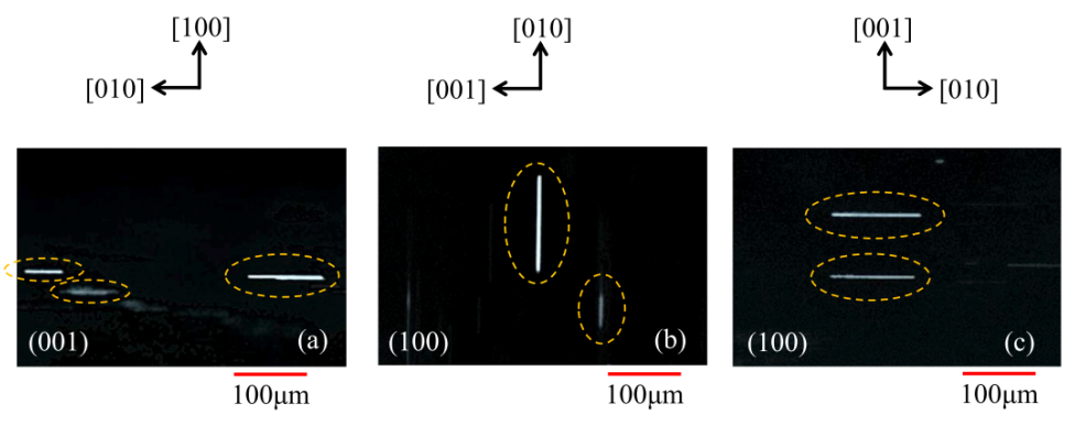
Fig. 1. Line-shaped defects on different crystal planes of β-Ga₂O₃ grown by the VB method [3].
Similar morphological defects have also been reported in β-Ga₂O₃ crystals grown by the EFG method. A representative example is nanopipe defects. Nanopipes can be understood as hollow, tube-like defects extending along specific crystallographic directions, typically aligned linearly along the [010] direction, as shown in Fig. 2.
It has been suggested that such defects may be associated with the decomposition of gallium oxide melt during high-temperature growth, the formation of volatile sub-oxide species, and local instability at the growth interface [4].
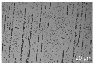
Fig. 2. Nanopipe defects in (001)-plane β-Ga₂O₃ crystals grown by the EFG method [4].
For the EFG method, nanopipe defects are not entirely uncontrollable. By optimizing the oxygen partial pressure, growth temperature, pulling rate, die design, and thermal field distribution, the probability of their formation can be reduced to some extent.
In other words, nanopipe defects not only reflect the intrinsic anisotropic nature of β-Ga₂O₃ crystals, but also highlight the stringent requirements for interface stability and ambient control during melt-growth processes.
Etch Pits: An Important Window for Identifying Dislocations, Voids, and Defect Origins
Etch pits are not defects themselves, but rather surface features revealed after selective chemical etching of crystalline defects. For β-Ga₂O₃ substrates, dislocations, voids, nanopipes, or regions of localized stress concentration are preferentially etched, leading to the formation of etch pits with distinct morphologies. Therefore, etch pit density is commonly used to evaluate crystal defect levels, while the morphology and distribution of etch pits can also provide clues for identifying defect types. However, since etch pit morphology is strongly influenced by crystallographic orientation and etching conditions, the true origin of defects usually needs to be further confirmed using techniques such as XRT and TEM.
As shown in Fig. 3, researchers selected a β-Ga₂O₃ crystal grown by the EFG (Edge-defined Film-fed Growth) with a main surface orientation of (−201), and performed selective etching on its (010) cross-section. Multiple typical etch pit morphologies were observed on the surface [5]. In the literature, these are often classified into different types based on morphological differences. Among them, some etch pits are associated with void-like defects, whose shapes evolve with increasing etching time. Others are related to dislocations and typically exhibit more stable and characteristic morphologies.
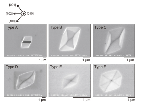
Fig. 3. Typical etch pit morphologies on the (010) plane of gallium oxide at the same location under different etching times [5].
It is important to note that etch pit morphology is strongly dependent on crystallographic orientation. For β-Ga₂O₃ substrates grown by the EFG method, the commonly observed etch pit morphologies on different principal planes are not identical.
For example, on the (−201) principal surface, “gourd-shaped” etch pits are often observed, whereas on the (001) surface, etch pits with a “bullet-like” morphology may appear. These differences reflect the strong influence of crystallographic anisotropy in β-Ga₂O₃ on both etching behavior and defect manifestation.
Similar variations in etch pit morphology can also be observed on different crystal planes of VB-grown crystals, as shown in Fig. 4. The shape, distribution, and density of etch pits on different planes can provide insight into the spatial distribution of defects inside the crystal and their relationship with the growth direction.
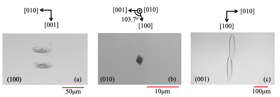
Fig. 4. Main etch pit morphologies on different crystal planes of β-Ga₂O₃ grown by the VB method [3].
Therefore, etch pits are not merely simple surface features, but an important entry point for understanding the defect structure of β-Ga₂O₃ crystals. By combining etch pit density statistics with techniques such as XRT and TEM, different defect types—such as dislocations, voids, and nanopipes—can be more accurately distinguished.
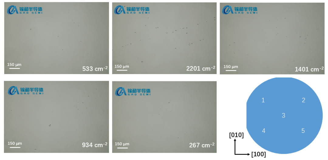
Fig. 5 shows the etch pit morphology and density distribution at different regions of a β-Ga₂O₃ substrate on the (001) plane fabricated by Gao Semi using the EFG method.
As shown in Fig. 5, after selective etching of different regions of the (001) β-Ga₂O₃ substrate prepared by the EFG method, the overall surface remains relatively smooth, with only a small number of isolated etch pits observed. The etch pit densities at five measured points are on the order of 10²–10³ cm⁻², with a minimum value of approximately 267 cm⁻². This indicates that the substrate exhibits good crystal quality and excellent in-plane uniformity, providing a solid foundation for subsequent homoepitaxial growth and device fabrication.
Processing-Induced Damage: Post-Growth Defects That Cannot Be Ignored
In addition to intrinsic defects formed during crystal growth, wafer processing steps can also introduce new damage. To transform β-Ga₂O₃ single crystals into usable wafers, multiple processes are required, including slicing, grinding, thinning, and chemical mechanical polishing (CMP). Due to the pronounced cleavage tendency and anisotropy of β-Ga₂O₃, mechanical processing can easily generate subsurface damage, scratches, microcracks, and localized stress concentrations.
As shown in Fig. 6, XRT characterization reveals line-shaped defects introduced during processing. The feature marked as “p” corresponds to line defects associated with processing-induced damage. These defects may not originate from the crystal growth process itself, but instead are formed during wafer slicing, grinding, or polishing steps.
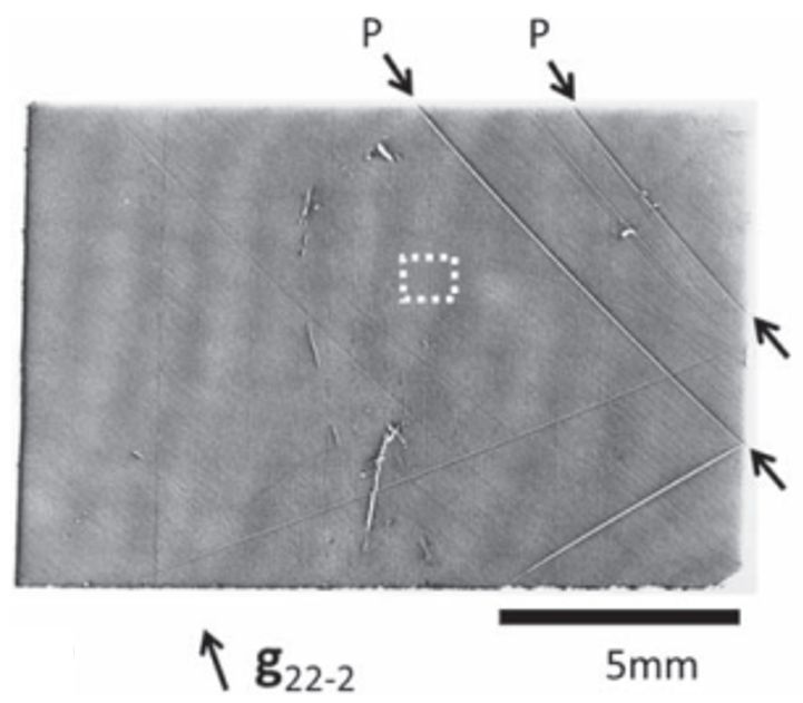
Fig. 6. Characterization results of processing-induced damage in the substrate [6].
The effects of processing-induced damage can sometimes be highly concealed. Even when the substrate surface appears relatively smooth after chemical mechanical polishing (CMP), a damaged layer may still remain beneath the surface. During subsequent high-temperature epitaxial growth, such damage can evolve into defect sources, degrading epitaxial layer quality. In device fabrication, it may also act as a localized leakage path or a dielectric breakdown.
Therefore, for gallium oxide substrates, defect control should not be limited to the crystal growth stage. It must extend throughout the entire processing chain, including wafer slicing, grinding, polishing, and cleaning. Optimizing processing parameters, reducing mechanical stress, controlling material removal, and improving surface cleanliness are all critical steps for enhancing substrate quality.
Impact of Defects on Devices: Defect Coupling and Leakage Paths
The impact of crystal defects on device performance is not simply determined by the total number of defects. For β-Ga₂O₃ substrates, more critical factors include the defect type, spatial orientation, propagation length, and whether the defects couple with current pathways and high-electric-field regions within the device.
In power devices, defects typically manifest as increased reverse leakage current and reduced breakdown voltage. Taking Schottky diodes as an example, under ideal conditions, reverse bias is mainly supported by the epitaxial drift layer, effectively blocking current flow. However, when defects such as dislocations, voids, or nanopipes exist in the substrate or epitaxial layer, they may introduce local barrier inhomogeneity, trap-assisted transport, or even continuous leakage pathways, allowing reverse current to pass more easily. Under high electric fields, defects can also induce local field crowding, increasing the risk of premature breakdown [7–8].
Dislocations are among the most critical defects affecting leakage in β-Ga₂O₃ devices. For β-Ga₂O₃ substrates with a (−201) orientation, studies have shown a clear correlation between dislocation-related etch pit density and the reverse leakage current of Schottky diodes, as shown in Fig. 7 [7]. In general, a higher dislocation density leads to higher reverse leakage current. This behavior may be attributed to deep-level defects, local strain fields, and impurity segregation around dislocations. These factors can modify the local barrier height, making dislocation regions preferential pathways for carrier transport.
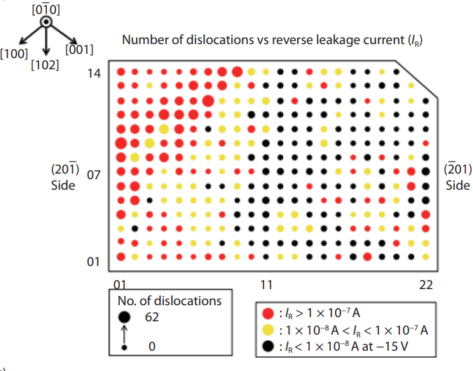
Fig. 7. Relationship between substrate defect density and reverse leakage current in Schottky diodes [7].
However, not all dislocations cause equally severe electrical impacts. Studies have shown that in β-Ga₂O₃ Schottky diodes, the influence of dislocations and other defects becomes significantly more pronounced when they are located beneath the Schottky contact, extend through the device current path, or couple with local high-electric-field regions [8–9]. Therefore, when evaluating the impact of defects, it is necessary to consider not only the defect type, but also its spatial location and its relationship with the device structure.
Spatial Distribution of Defects and Leakage Risk
The impact of voids and nanopipe-type defects depends strongly on their spatial orientation and propagation length. In β-Ga₂O₃, some voids and nanopipes extend along the [010] direction; however, the relationship between the [010] direction and the device current flow varies significantly depending on the substrate orientation. As a result, defects extending along the same crystallographic direction may have completely different electrical impacts on substrates with different orientations.
For example, in (001) and (−201) substrates, defects extending along the [010] direction are often approximately parallel to the substrate surface. If such defects do not penetrate the vertical current path of the device, their impact on reverse leakage may be relatively limited. In contrast, in (010) substrates, voids extending along the [010] direction are more likely to traverse the substrate. When such defects are sufficiently long and connect the front and back sides of the device, they may form effective leakage pathways, leading to a significant increase in reverse current.
Therefore, when evaluating the impact of voids or nanopipes, it is not sufficient to consider only their presence; it is also essential to assess whether they “penetrate” the device active region. For vertical devices, through-type defects are more likely to form leakage channels from the front side to the backside. For lateral devices, it is necessary to further consider the channel position, electrode edges, gate edges, and local electric field distribution to determine whether defects will participate in carrier transport or induce localized leakage.
Substrate Defects and Epitaxial Quality
In addition to directly forming leakage paths, defects can also indirectly affect device performance by degrading epitaxial quality.
For β-Ga₂O₃ homoepitaxy, defects in the substrate—such as dislocations, nanopipes, voids, and processing-induced damage—may be replicated into the epitaxial layer during growth. They may also trigger the formation of new extended defects or local morphological anomalies at the growth interface. However, under certain growth conditions, some defects may be transformed or even partially suppressed. Therefore, the relationship between substrate defects and epitaxial defects is not a simple one-to-one correspondence, but instead must be evaluated in conjunction with crystallographic orientation, growth method, and specific process conditions.
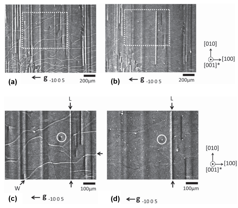
Fig. 8. Comparison of X-ray topography of the same region on a (001)-oriented EFG substrate before and after HVPE epitaxy [6].
For high-voltage power devices, the epitaxial drift layer typically takes on the primary voltage-blocking function. If inherited defects, line defects, local pits, or surface roughening exist in the epitaxial layer, they may alter the local electric-field distribution and increase reverse leakage or the risk of premature breakdown, thereby degrading device uniformity and reliability. Therefore, substrate defect control is not only critical for substrate quality itself, but also plays a key role in the evolution of defects during epitaxial growth and in the resulting device performance.
Processing Damage and Interface Quality
Processing-induced damage should also not be overlooked. Subsurface damage generated during slicing, grinding, and CMP processes may remain within the near-surface region of the substrate even when the surface appears smooth. During high-temperature epitaxial growth, such damage can act as sources for defect propagation, and may also affect metal contacts, interface state density, and surface leakage. For Schottky diodes and field-effect transistors, surface and interface quality directly determines barrier uniformity, gate dielectric reliability, and device stability.
Defect Traps and Long-Term Reliability
From a reliability perspective, the impact of defects may further amplify over long-term operation. Under high temperature, high voltage, or strong electric field conditions, defect-related trap states can repeatedly capture and release carriers, leading to current drift, threshold voltage shift, hysteresis, or degradation of dynamic performance. Localized leakage regions may also cause heat accumulation, increasing the risk of progressive device degradation during extended operation.
Conclusion
In this issue, we reviewed defects in β-Ga₂O₃ substrates grown by melt-growth methods and their impacts on device performance. Overall, defect behavior in β-Ga₂O₃ is closely related to its low-symmetry crystal structure and strong anisotropy. Many defects are not randomly distributed but exhibit pronounced directional characteristics. Therefore, when evaluating substrate quality, it is insufficient to consider only defect density; a comprehensive assessment must also take into account defect type, spatial orientation, propagation length, and crystallographic plane.
From a device perspective, defect effects are also not simply a matter of “defects inevitably causing failure.” Dislocations may increase reverse leakage through local trap states, strain fields, or barrier inhomogeneities. The impact of voids and nanopipes depends strongly on whether they penetrate the device current path. Processing-induced damage, although introduced after crystal growth during wafer preparation, may continue to evolve during subsequent epitaxy and device fabrication, affecting epitaxial quality, interface properties, and device reliability.
Defect research in gallium oxide substrates is therefore not only about “seeing defects,” but more importantly about understanding how they influence epitaxial growth and device performance. As substrate sizes continue to scale up, defect control will become a critical factor determining epitaxial quality, device yield, and long-term reliability.
Reference:
[1] Z. Galazka, IEEE Trans. Electron Devices, 2025.
[2] S. J. Pearton et al., Appl. Phys. Rev. 5, 011301 (2018).
[3] E. Ohba, T. Kobayashi, T. Taishi, K. Hoshikawa, J. Cryst. Growth 556, 125990 (2021).
[4] P. Wang, Q. Yin, B. Chen, Y. Dong, Y. Li, W. Mu, Appl. Phys. Lett. 127, 062101 (2025).
[5] K. Hanada, T. Moribayashi, K. Koshi et al., Jpn. J. Appl. Phys. 55, 1202B (2016).
[6] S. Masuya, K. Sasaki, A. Kuramata, S. Yamakoshi, O. Ueda, M. Kasu, Jpn. J. Appl. Phys. 58, 055501 (2019).
[7] M. Kasu, K. Hanada, T. Moribayashi, A. Hashiguchi, O. Ueda, Jpn. J. Appl. Phys. 55, 1202BB (2016).
[8] T. Oshima, A. Hashiguchi, T. Moribayashi, K. Koshi, K. Sasaki, A. Kuramata, O. Ueda, T. Oishi, M. Kasu, Jpn. J. Appl. Phys. 56, 086501 (2017).
[9] B. Fu, K. Fu, Z. Jia, W. Mu, Y. Yin, J. Zhang, X. Tao, J. Semicond. 40, 011804 (2019).
Instruction
Official Account

Cooperation
Top
