


From June 25 to 27, 2026, the 2026 China Symposium on Power Semiconductor Devices and ICs (CSPSD 2026) was held at the Hyatt Regency Shanghai Lingang. As one of the leading exhibitors in gallium oxide materials and equipment, Hangzhou Fujia Gallium Technology Co., Ltd. received the conference's Outstanding Technical Innovation Product Award for its 12-inch VB-grown Ga₂O₃ single-crystal ingot. During the conference, Chairman and Founder Researcher Hongji Qi delivered a keynote presentation outlining the industrial potential of gallium oxide materials and the technological pathway of vertical Bridgman (VB) crystal growth. Meanwhile, the company showcased a broad portfolio of gallium oxide products at the exhibition, where its booth attracted continuous visitor traffic and its technological achievements drew strong interest from stakeholders across the industry value chain.
Receives the Outstanding Technical Innovation Product Award
Fujia's VB Crystal Growth Milestones
2023 – Strategic Initiation
2024 – Breakthroughs in 3-inch and 4-inch Crystal Growth
2025 – Breakthroughs in 6-inch and 8-inch Crystal Growth
2026 – Breakthrough in 12-inch Crystal Growth
In the field of Vertical Bridgman (VB) growth of Ga₂O₃ single crystals, Hangzhou Fujia Gallium Technology Co., Ltd. has consistently achieved new size milestones every few months, establishing itself as the clear leader in both China's and the global VB-grown gallium oxide crystal sector. This remarkable pace of technological advancement once again received high industry recognition at the 2026 China Symposium on Power Semiconductor Devices and ICs (CSPSD 2026), where Fujia Gallium 's 12-inch VB-grown Ga₂O₃ single-crystal ingot was honored with the conference's Outstanding Technical Innovation Product Award.
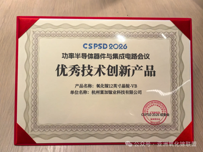
▲ CSPSD 2026 Outstanding Technical Innovation Product Award Certificate
Behind this rapid pace of advancement lies Fujia Gallium's comprehensive in-house expertise in the vertical Bridgman (VB) growth technology. From thermal field design and precise temperature-gradient control to crucible material selection and continuous optimization of growth parameters, the company has independently developed a fully automated VB crystal growth system, enabling precise control over the entire crystal growth process. This fully self-developed platform has allowed Fujia Gallium to push the size limit of VB-grown Ga₂O₃ single crystals to an unprecedented 12 inches, while much of the industry remains in the exploratory stage of 6-inch crystal growth.
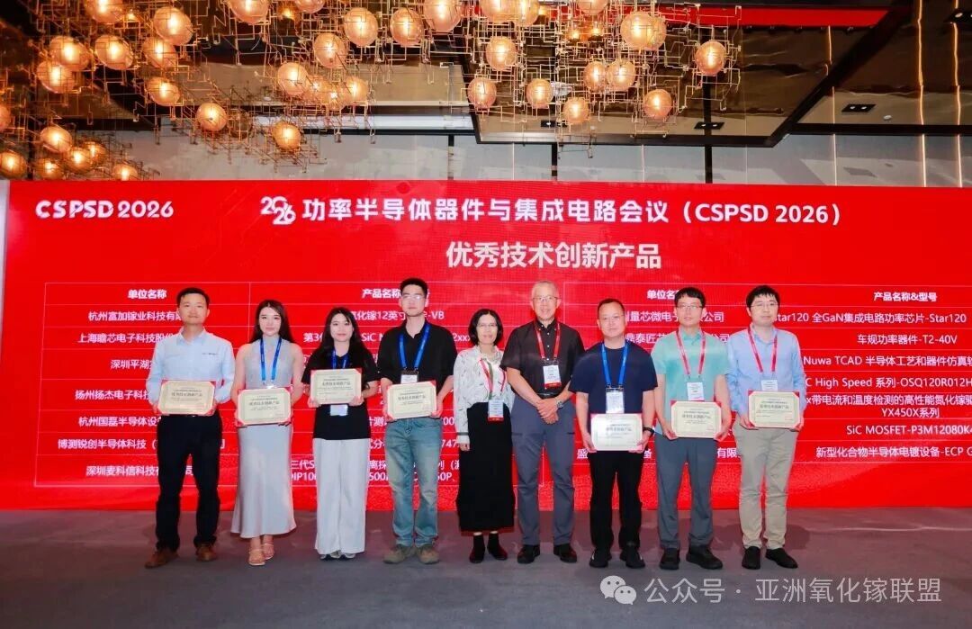
▲ CSPSD 2026 Outstanding Technical Innovation Product Award Presentation Ceremony
Compared with 6-inch wafers, a single 12-inch wafer can produce approximately four times as many chips, significantly reducing manufacturing costs through improved economies of scale. More importantly, the 12-inch format is fully compatible with existing silicon-based semiconductor manufacturing lines, enabling downstream manufacturers to transition to Ga₂O₃ device production without major equipment upgrades. This compatibility is expected to substantially accelerate the commercialization of Ga₂O₃ power devices.
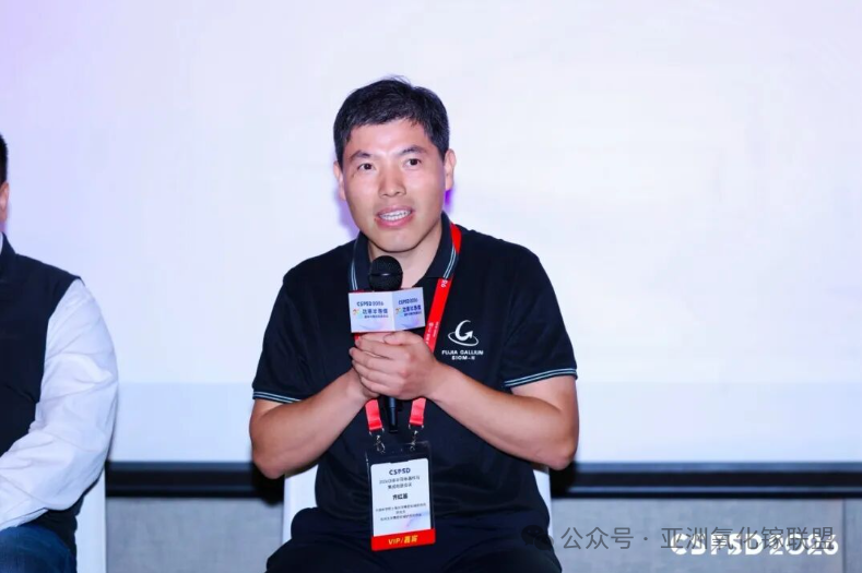
▲ Researcher Hongji Qi Participates in the CSPSD 2026 Panel Discussion
During his keynote presentation, Researcher Hongji Qi, Chairman of Fujia Gallium, highlighted the industrial potential of Ga₂O₃ with a set of compelling figures: its theoretical critical breakdown electric field is approximately 27 times that of silicon and three times that of silicon carbide, making it one of the most promising materials for next-generation high-voltage power devices. He also emphasized that lowering costs while enhancing performance is the key to large-scale commercialization, and that Fujia Gallium's breakthrough in 12-inch crystal technology represents the company's answer to this challenge.
Diverse Product Portfolio Draws Attention, with 12-inch Single Crystal Taking Center Stage
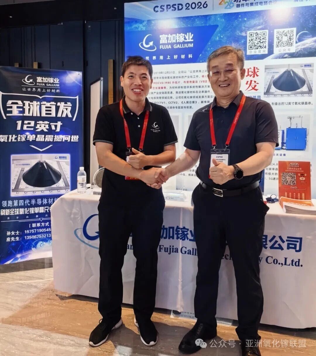
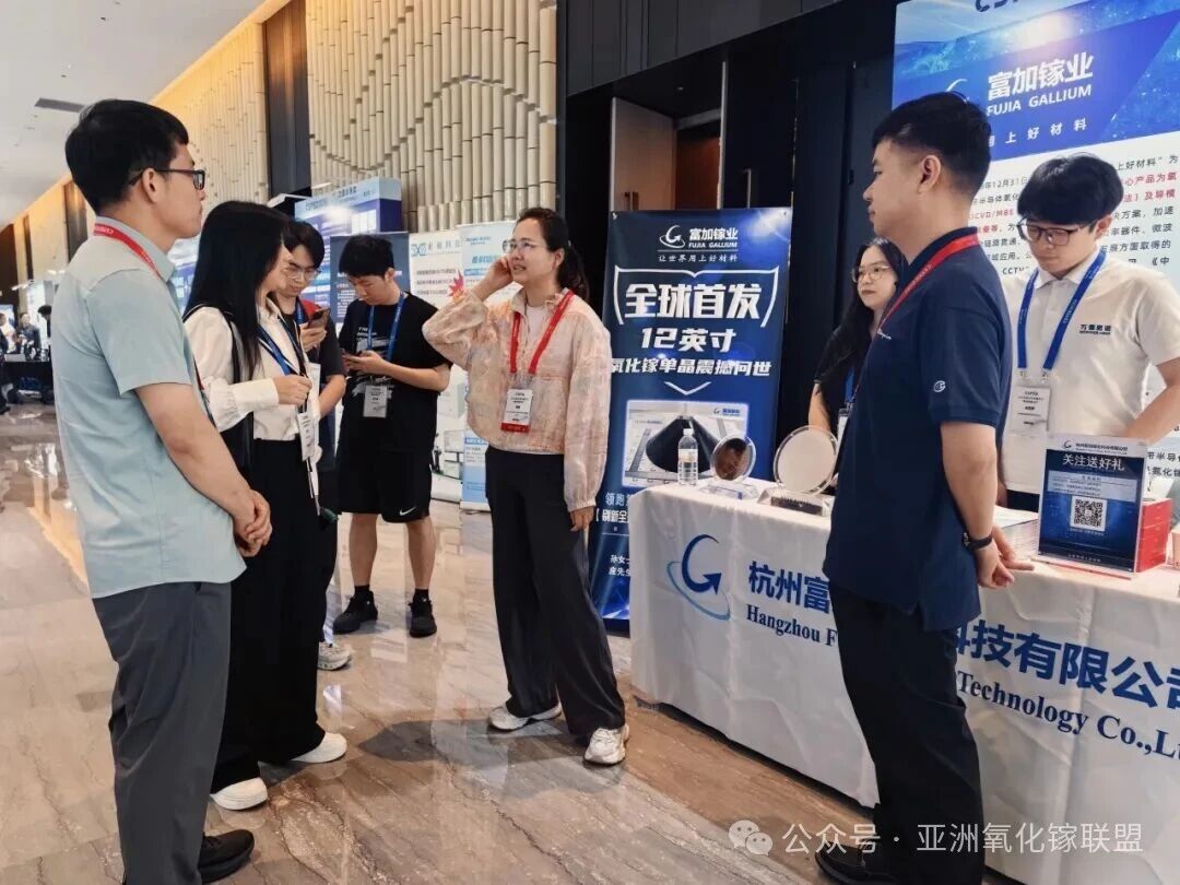
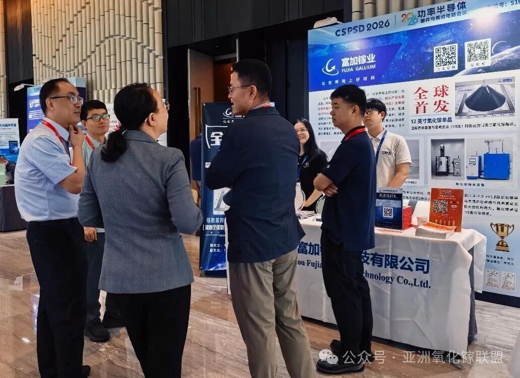
At the exhibition, Fujia Gallium showcased its core product portfolio, including Ga₂O₃ single-crystal substrates, MOCVD and MBE epitaxial wafers, and crystal growth equipment. While the company's 12-inch VB-grown Ga₂O₃ single crystal attracted widespread attention, visitors also expressed strong interest in its independently developed "AI One-Click Crystal Growth" technology and intelligent growth systems. By deeply integrating artificial intelligence with crystal growth, this innovative approach represents an important step forward in semiconductor material manufacturing.
Industry, Academia, Research, and End Users Converge to Foster Broad Collaboration
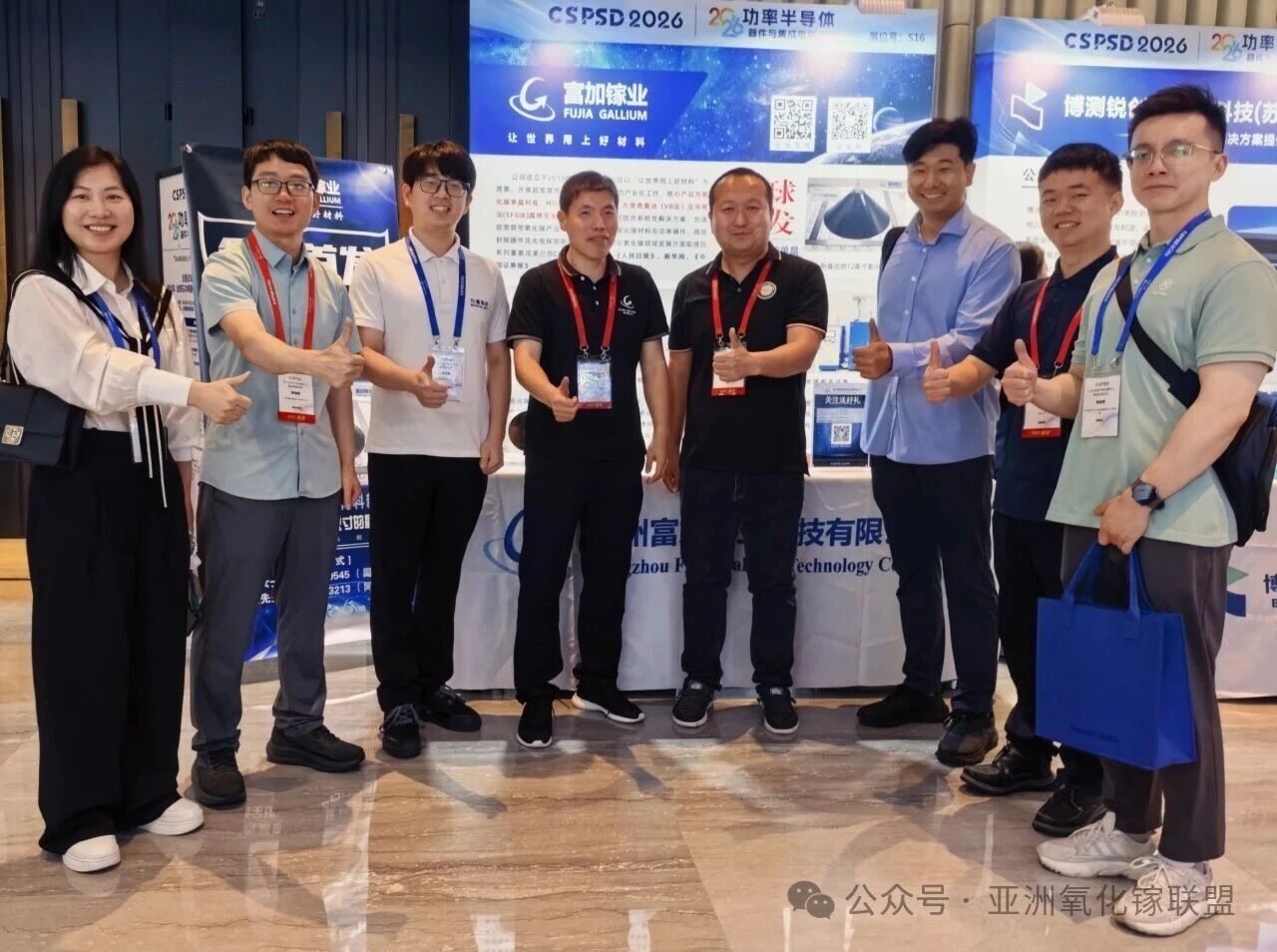
Throughout the three-day event, Fujia Gallium's booth remained a hub of continuous discussion and engagement. Device manufacturers, packaging and testing companies, research institutions, and other partners from across the semiconductor value chain held in-depth exchanges with the Fujia Gallium team on topics including Ga₂O₃ substrate supply capacity, epitaxial wafer performance, and customized crystal growth equipment. These discussions resulted in a broad range of intentions for future collaboration.
CSPSD 2026 not only provided a valuable platform for Fujia Gallium to showcase its latest technological achievements, but also created new opportunities to strengthen partnerships and advance the Ga₂O₃ industry together.
Committed to bringing better materials to the world, Fujia Gallium looks forward to building the future of the gallium industry together with partners worldwide.
Product Portfolio
Gallium Oxide Crystal Growth Equipment
Fujia Gallium has developed the world’s first EFG crystal growth system featuring a proprietary “one-click crystal growth” function, supporting 2-inch to 8-inch crystal production. The system is protected by 6 granted domestic patents and 4 international patents. Complete equipment solutions and process packages are available. The company has also independently developed fully automated VB (Vertical Bridgman) crystal growth equipment and was the first in China to overcome the technical bottleneck of 12-inch Ga₂O₃ single-crystal growth using the VB method, enabling the production of large-diameter bulk crystals. Currently, this equipment has been granted 6 domestic patents and 4 international patents, and VB systems along with process packages can be provided based on customer requirements.
Gallium Oxide Single-Crystal Substrates
As one of China’s earliest pioneers in Gallium Oxide single-crystal research and an industry-leading supplier, Fujia Gallium provides high-quality single-crystal substrates to global customers. The product portfolio includes 26 standard Ga₂O₃ substrate specifications covering diameters from 2 to 8 inches. Customized solutions are available in terms of wafer size, electrical properties, and crystal orientation, supporting both advanced epitaxy R&D and volume production requirements.
Gallium Oxide Epitaxial Wafers
Built upon mature MOCVD (Metal-Organic Chemical Vapor Deposition) and MBE (Molecular Beam Epitaxy) platforms, Fujia Gallium offers 15 standard epitaxial wafer products from 2-inch to 6-inch formats, as well as customized MBE-based epitaxial structures. The company provides integrated “substrate + epitaxy” solutions. A precise process control system enables customization of key parameters including epitaxial layer thickness, doping concentration, and compositional uniformity, meeting diverse requirements across different power levels and device architectures.
About Hangzhou Fujia Gallium
Hangzhou Fujia Gallium Technology Co., Ltd., established on December 31, 2019, is committed to its mission of “Bringing Better Materials to the World” and focuses on the industrialization of ultra-wide bandgap Gallium Oxide semiconductor materials. Its core products include Gallium Oxide single-crystal substrates, MOCVD/MBE epitaxial wafers, and crystal growth equipment based on the Vertical Bridgman (VB) and Edge-Defined Film-Fed Growth (EFG) methods. The company provides systematic solutions for material development, accelerating the integration of the entire ultra-wide bandgap Gallium Oxide industry chain and promoting the application of Gallium Oxide materials in power devices, microwave RF devices, and optoelectronic detection. A series of major achievements in Gallium Oxide development have been featured by leading media outlets including CCTV, People’s Daily, Xinhua News Agency, China Securities Journal, and The Paper. In terms of corporate recognition, the company was designated as a Zhejiang Province Science and Technology SME in 2022, recognized as a National High-Tech Enterprise in 2023, and awarded the titles of Hangzhou High-Tech Enterprise R&D Center and Zhejiang “Specialized and Sophisticated” SME in 2024. In 2025, it obtained ISO 9001 Quality Management System certification (Certificate No. 20225Q20294R0M) and was also named a 2024 Hangzhou “Rising Eagle” Enterprise. In the Gallium Oxide field, the company is leading the drafting of the first national standard in this area and has undertaken one project from the National Development and Reform Commission and one from the Ministry of Industry and Information Technology, while participating in three additional national and provincial-level projects supported by the National Natural Science Foundation of China and regional authorities in Zhejiang and Shanghai. To date, the company has been granted 14 international patents (6 in the United States, 7 in Japan, and 1 in Europe), 42 domestic patents, three registered “Fujia Gallium” trademarks, and five software copyrights, including its proprietary “One-Click Crystal Growth” control software.
Instruction
Official Account

Cooperation
Top
