


At present, the fourth-generation semiconductor industry is rapidly transitioning from laboratory research to engineering applications. In response to the growing demand from both academia and industry for high-quality epitaxial wafers, Hangzhou Garen Semiconductor Co., Ltd. (hereinafter referred to as "Garen Semiconductor") has officially launched its new high-performance Ga₂O₃ thin-film epitaxial wafers, building upon its previous breakthroughs in thick-film epitaxial technology. The new product provides high-quality epitaxial materials to support the development of next-generation power and RF devices.
Technical Highlights of the Thin-Film Epitaxial Wafers
1. Crystal Quality Reaches an Internationally Advanced Level.
The full width at half maximum (FWHM) of the X-ray diffraction (XRD) rocking curves measured at five locations across the wafer is consistently below 30 arcsec, confirming a low epitaxial defect density and excellent crystalline integrity. This provides a solid foundation for achieving high carrier mobility in device applications. As a result, electrons can be transported more efficiently through the material, enabling stable operation at higher frequencies while simultaneously enhancing RF performance and power conversion efficiency.
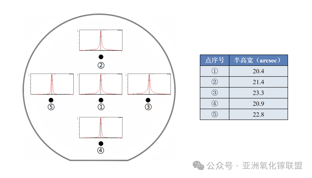
Figure 1. XRD Rocking Curves and Corresponding Measurement Results at Five Wafer Locations for Garen Semiconductor's Thin-Film Epitaxial Wafer
2. Excellent Surface Flatness for Advanced Device Fabrication.
Atomic force microscopy (AFM) measurements show a surface roughness of only 0.35 nm, meeting the stringent planarity requirements of precision fabrication processes such as photolithography and etching. The exceptionally smooth surface helps minimize process variations, improve device yield, enhance pattern transfer accuracy, and ultimately ensure greater device uniformity and reliability.
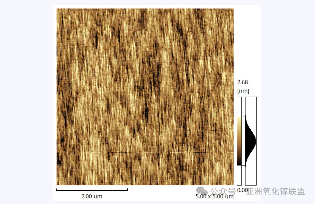
Figure 2. AFM Image of Garen Semiconductor's Thin-Film Epitaxial Wafer
3. Excellent Electrical Performance with Strong Process Compatibility.
The standard epitaxial wafers exhibit a high electron mobility of 130–184 cm²/V·s, ensuring stable and reproducible electrical characteristics for device fabrication. In addition, the carrier concentration can be flexibly tailored to customer requirements, enabling optimization for a wide range of applications, including power devices and RF devices. This customization capability helps meet diverse performance targets and accelerates customers' device development and optimization processes.
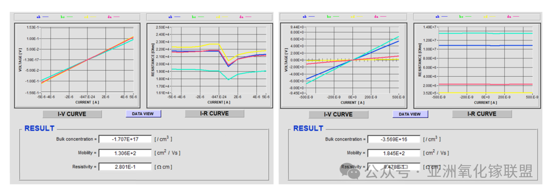
Figure 3. Hall Measurement Results of Garen Semiconductor's Thin-Film Epitaxial Wafer
Product Specification
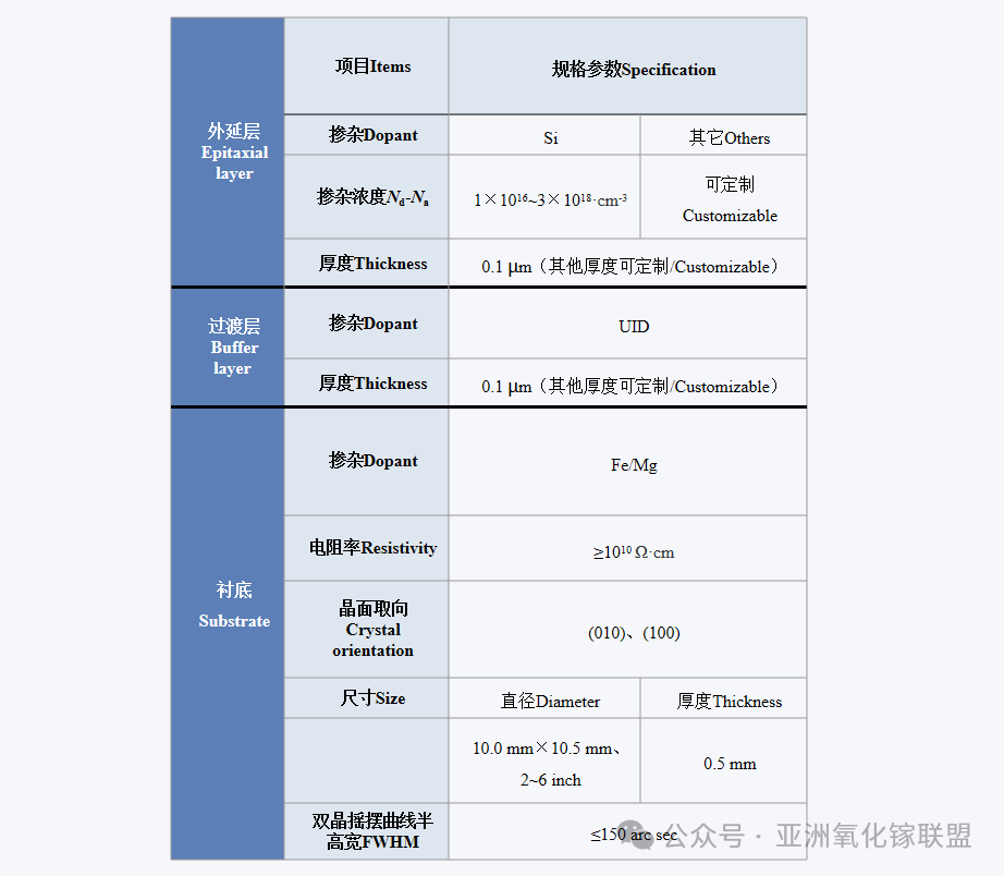
Figure 4. Product Specification Sheet for Garen Semiconductor's Thin-Film Epitaxial Wafers
The substrate orientation, epitaxial layer thickness, carrier concentration, and other key parameters can be customized to meet customers' specific device design requirements. For more information about the product or customized solutions, please contact our sales and technical support team.
Driving Innovation at the Speed of Gallium
The breakthrough in high-quality thin-film epitaxy enables Ga₂O₃ devices to operate reliably under higher power and higher voltage conditions. In power electronics, it helps reduce conduction losses and improve power conversion efficiency. In RF communications, it supports the development of high-power RF devices, providing a solid material foundation for next-generation applications such as 5G/6G communications and radar systems.
Leveraging proprietary core technologies spanning the entire value chain—from crystal growth to thin-film epitaxy—Garen Semiconductor continues to accelerate the transition of Ga₂O₃ materials from laboratory research to industrial applications. The new thin-film epitaxial wafers are now available for pre-order. We sincerely welcome universities, research institutes, and device manufacturers to collaborate with us in unlocking the full potential of Ga₂O₃ and advancing the development of the fourth-generation semiconductor industry.
For more information about Garen Semiconductor and its products, please visit our official website: http://garen.cc/
Or contact us via the following ways:
Mr. Jiang: +86 15918719807
E-mail: jiangjiwei@garen.cc
Mr. Xia: +86 19011278792
E-mail: xianing@garen.cc
Instruction
Official Account

Cooperation
Top
