


Introduction

Working in close collaboration with the research team led by Professor Xutang Tao at the State Key Laboratory of Crystal Materials, Shandong University, the company is dedicated to the research, development, and commercialization of novel functional crystal materials with significant application potential. Its core business focuses on fourth-generation ultra-wide-bandgap gallium oxide (Ga₂O₃) substrate materials, which serve as the foundation for high-performance power electronic and optoelectronic devices. These devices are expected to find broad applications in new energy vehicles, high-speed rail, solar-blind ultraviolet detection, 5G communications, smart grids, wind power generation, and high-voltage power transmission and distribution.
The company is also engaged in the development and commercialization of specialty single-crystal optical fiber sensors for extreme environments. Featuring outstanding resistance to high temperatures, high pressure, radiation, and corrosion, these specialty oxide crystal fibers enable the fabrication of temperature, pressure, displacement, and vibration sensors for health monitoring in demanding applications such as aircraft engines, nuclear reactors, and rocket launch facilities.
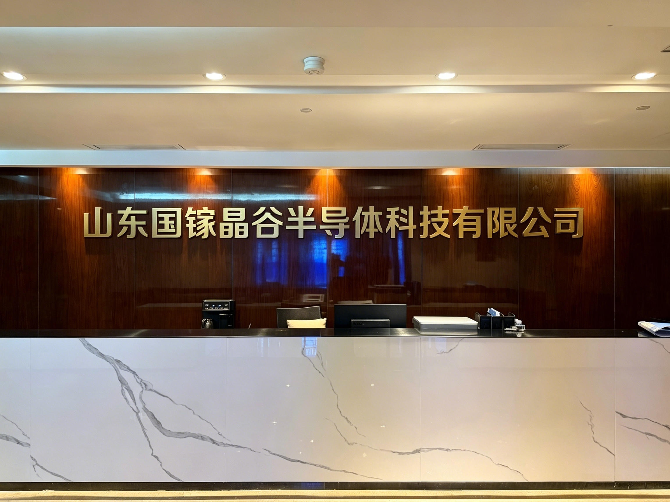
Research System
The team has established a comprehensive theoretical and technological framework for the growth of fourth-generation ultra-wide-bandgap Ga₂O₃ substrate and epitaxial materials, as well as for device architecture and fabrication processes in China. This integrated innovation system has enabled major original breakthroughs spanning core equipment, materials, and devices, advancing China's fourth-generation ultra-wide-bandgap Ga₂O₃ materials and devices to the international forefront. It also marks a significant transition from technological self-reliance to innovation-driven development in China's fourth-generation semiconductor industry.
Team Overview
The company leverages the expertise of Professor Xutang Tao's research team to conduct the research, production, and commercialization of EFG-grown Ga₂O₃ single-crystal substrates.
Professor Xutang Tao is the former Director of the State Key Laboratory of Crystal Materials at Shandong University and currently serves as a Chair Professor, Ph.D. supervisor, and academic leader of the laboratory. He is a recipient of the Changjiang Scholars Program Distinguished Professorship and the National Science Fund for Distinguished Young Scholars. Since returning to China in 2002 to establish his research team, Professor Tao has been dedicated to the full-chain research and development of functional crystal materials and devices.
He previously served as Director of the Institute of Crystal Materials and Director of the State Key Laboratory of Crystal Materials at Shandong University, and was a member of the 6th and 7th Defense Science and Technology Division of the Science and Technology Committee of the Ministry of Education. Professor Tao has published more than 400 papers in leading international journals and has received numerous prestigious awards, including the First Prize of the Ministry of Education Science and Technology Progress Award, the Second Prize of the Ministry of Education Natural Science Award, and the First Prize of the Shandong Provincial Science and Technology Progress Award.
Key Research Directions and Development Strategy of SINOGa Valley
Supported by the State Key Laboratory of Crystal Materials at Shandong University, the team was among the first in China to establish an industrialization roadmap for EFG (Edge-Defined Film-Fed Growth) technology for β-Ga₂O₃. Its research focuses on large-diameter single-crystal growth, precision doping, and epitaxial materials. Centered on the EFG crystal growth process, the team has developed a comprehensive technology platform spanning the entire industrial chain, from single-crystal growth, precision doping, and substrate processing to epitaxial films and power/solar-blind ultraviolet devices.
Three Core Research Directions
1.Large-Diameter β-Ga₂O₃Single-Crystal Growth (Core Business)
EFG (Edge-Defined Film-Fed Growth) Technology:
The team specializes in the growth of (001)-oriented β-Ga₂O₃ single crystals using the EFG method. It has achieved stable mass production of 2-inch and 4-inch single crystals. Its 4-inch (001) substrates feature twin-free crystals, an XRD rocking-curve FWHM below 58 arcsec, and a dislocation density of approximately 1 × 10⁴ cm⁻², representing a leading benchmark for EFG-grown Ga₂O₃ in China. The team is currently developing 6-inch (001) zero-twin single crystals, with small-batch sample deliveries to downstream partners planned for 2026.
2.Precision Doping Technologies (Conductive and Semi-Insulating Substrates)
Sn-Doped n-Type Conductive Substrates:
The team has developed technologies based on substitutional Sn doping and vacancy–impurity complex engineering to achieve highly uniform wafer resistivity for high-voltage Schottky diodes and MOS devices. Doping concentrations are optimized through the combination of first-principles simulations and experimental validation, enabling resistivity control over a range of 10⁻³ to 10 Ω·cm.
Fe-Doped Semi-Insulating Substrates:
Using deep-level Fe compensation doping, the team produces semi-insulating substrates with resistivities of ≥10¹⁰ Ω·cm, designed for solar-blind ultraviolet focal-plane arrays and RF devices. It has also addressed key challenges related to dopant uniformity and edge resistivity variation in large-diameter crystal ingots.
3.Crystal Defect Engineering and Precision Substrate Processing
①Investigation of the formation mechanisms of dislocations, twins, oxygen vacancies, and crystal cracking, together with the development of an AI-powered intelligent dislocation inspection system for rapid and automated wafer defect characterization.
②Precision wafer grinding and polishing technologies with optimized TTV (Total Thickness Variation), Bow, and Warp, achieving a surface roughness (Ra) below 0.2 nm, meeting epitaxy-grade substrate requirements.
③Development of dedicated processing technologies for (001), (010), and (100) crystal orientations.
The company currently supplies high-quality 2-inch, 4-inch, and 6-inch β-Ga₂O₃ single crystals and doped crystals that are free of cracking and twinning. The crystals exhibit excellent structural integrity, high uniformity and transparency, and are free from macroscopic defects such as bubbles and inclusions, achieving a leading level both domestically and internationally.
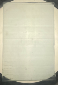
2-inch Bulk Ga₂O₃ Single Crystal
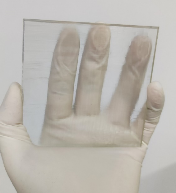
4-inch Bulk Ga₂O₃ Single Crystal
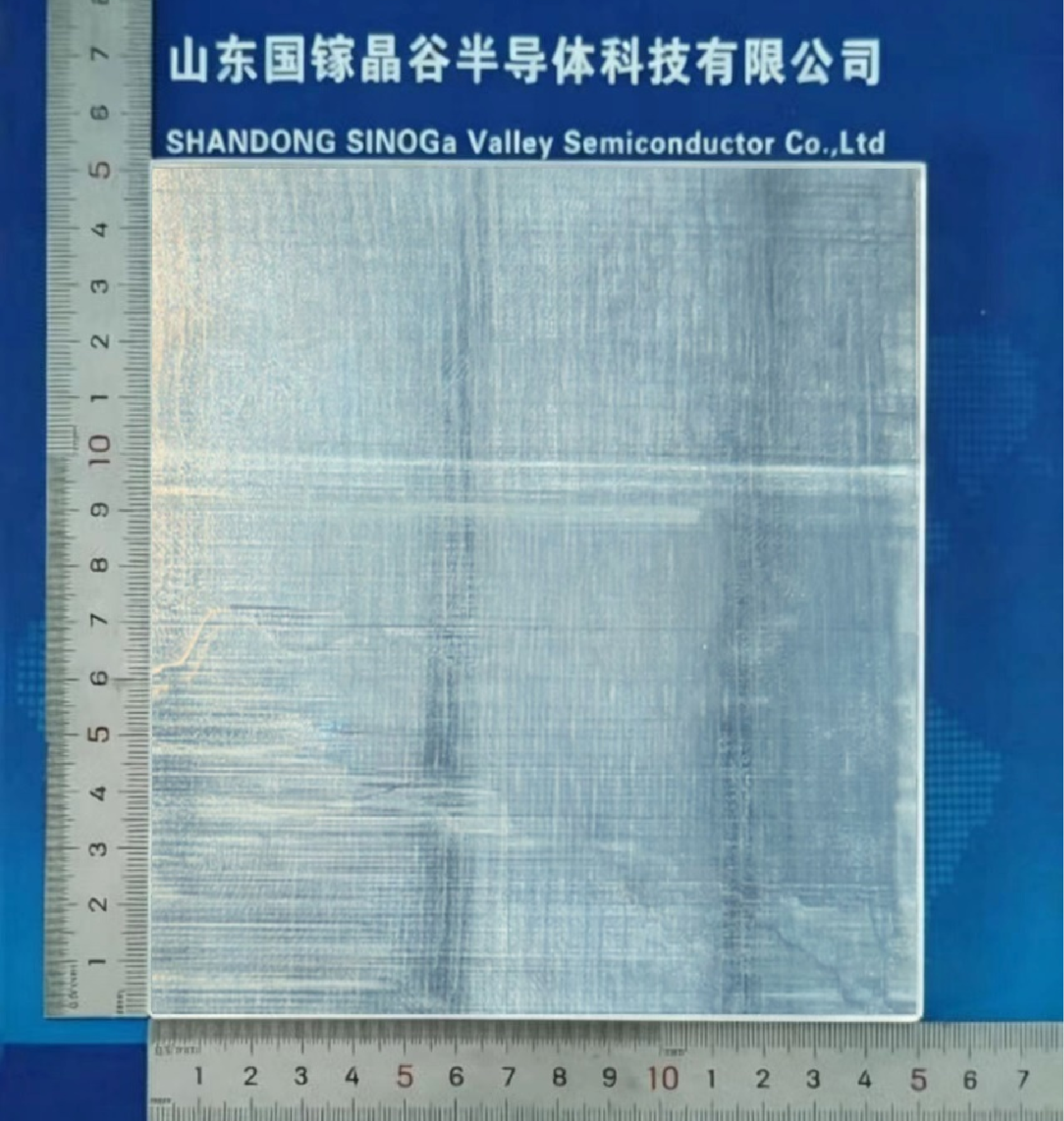
6-inch Bulk Ga₂O₃ Single Crystal
Products & Services
Ga₂O₃Single Crystals (Multiple Sizes)
Ga₂O₃Epitaxial Wafers (Multiple Sizes)
Dedicated Ga₂O₃Crystal Growth Equipment
Customized Crystal Solutions & Technical Support
Website:
www.ultragao.com
Instruction
Official Account

Cooperation
Top
