


Researchers from Japan Fine Ceramics Center have published a dissertation titled "Sub-resolution detectability of nanoscale surface defects in β-Ga₂O₃" in APL Materials.
Background
β-Ga₂O₃ is a core substrate material for next-generation high-power semiconductors due to its high Baliga’s figure of merit and melt-grown large-size wafers. Nanoscale surface defects such as pits and scratches degrade device leakage and breakdown voltage, requiring rapid, non-destructive large-area inspection. Conventional optical inspection methods rely on surface height contrast and cannot visualize sub-diffraction-limit defects or crystal dislocations simultaneously. Although phase-contrast microscopy can image dislocations, the quantitative relationship between defect geometry and detection limit remains unclear, without analytical models to predict detectable threshold, which hinders industrial non-destructive inspection of β-Ga₂O₃ wafers.
Abstract
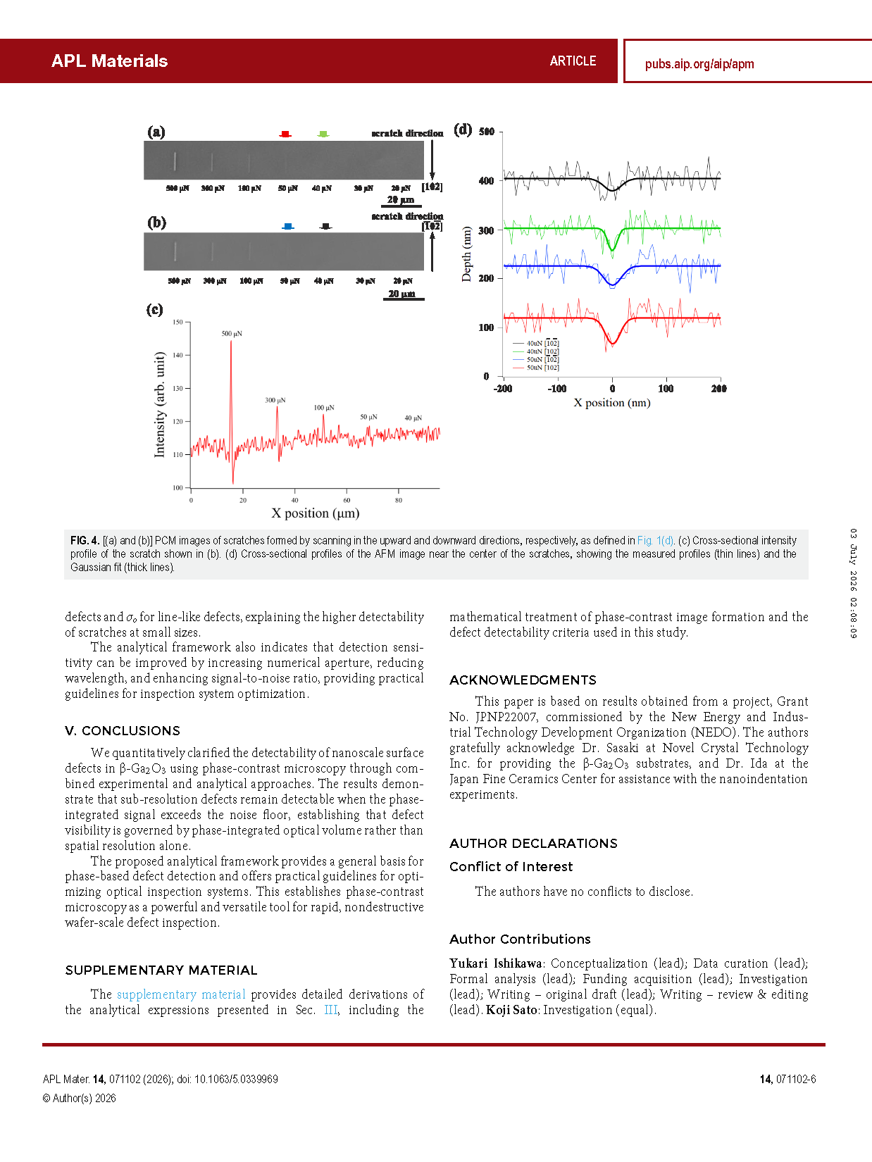
We quantitatively investigate the detectability of nanoscale surface defects in β-Ga₂O₃ using phase-contrast microscopy. Surface depressions with depths of ∼40–50 nm are shown to remain detectable even when their lateral dimensions are well below the diffraction limit. An analytical framework based on Gaussian defect profiles and diffraction-limited imaging theory accurately reproduces the observed detection boundary. The results demonstrate a general principle that defect detectability is governed by the phase signal integrated over the point spread function rather than by spatial resolution alone. This framework establishes a general principle for phase-based defect detection and provides practical guidelines for optimizing optical inspection systems for wide-bandgap semiconductors.
Highlights
Quantitatively characterize sub-resolution nano-pits and nano-scratches on β-Ga₂O₃via phase-contrast microscopy.
Establish Gaussian-based analytical model to predict detection limit of line/point type surface defects.
Reveal that integrated phase signal instead of spatial resolution dominates defect detectability.
Conclusion
We quantitatively clarified the detectability of nanoscale surface defects in β-Ga₂O₃ using phase-contrast microscopy through combined experimental and analytical approaches. The results demonstrate that sub-resolution defects remain detectable when the phase integrated signal exceeds the noise floor, establishing that defect visibility is governed by phase-integrated optical volume rather than spatial resolution alone.
The proposed analytical framework provides a general basis for phase-based defect detection and offers practical guidelines for optimizing optical inspection systems. This establishes phase-contrast microscopy as a powerful and versatile tool for rapid, nondestructive wafer-scale defect inspection.
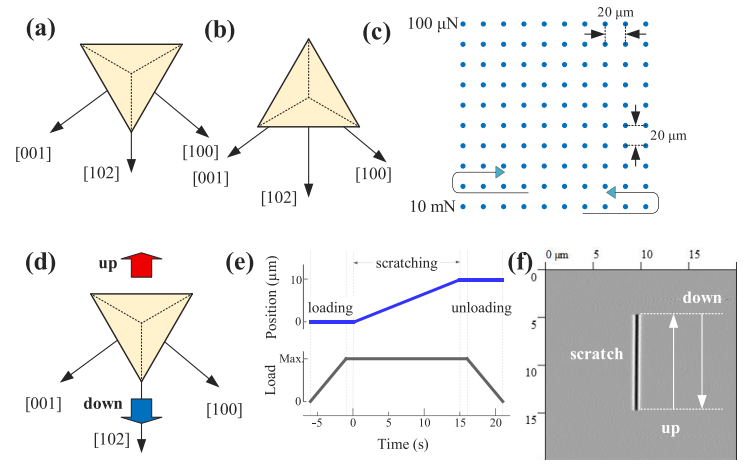
FIG. 1. [(a) and (b)] Schematic illustrations of the relationship between the Berkovich indenter and crystal orientation during indentation. (c) Formation pattern of indentation arrays. (d) Schematic of the relationship among the Berkovich indenter, crystal orientation, and scanning direction during scratch formation. (e) Temporal variation of indenter position and applied load during scratching. (f) AFM image of the fabricated scratch.
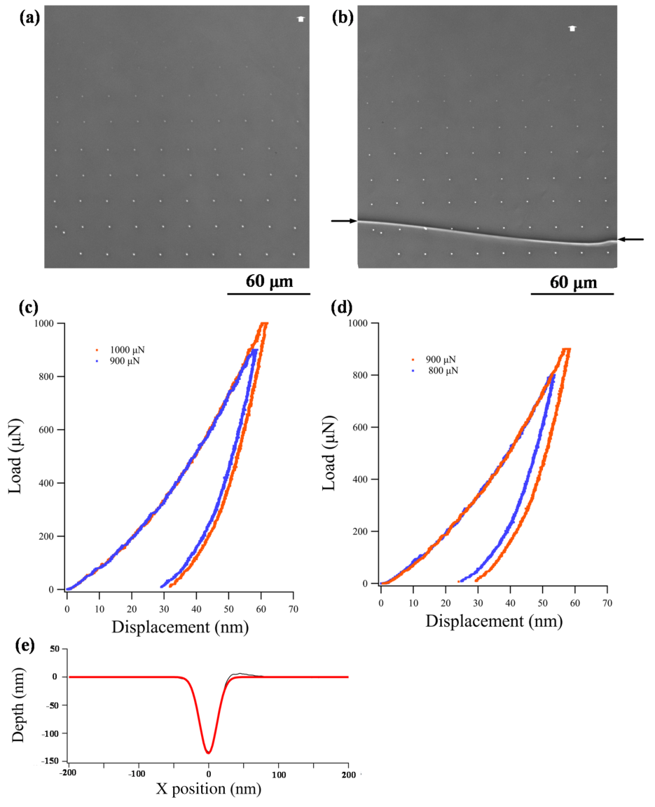
FIG. 2. [(a) and (b)] PCM images of indentation arrays formed under the indenter–crystal orientation configurations shown in Figs. 1 (a) and 1 (b), respectively. [(c) and (d)] Corresponding load–displacement curves obtained under the same conditions as in Figs. 1 (a) and 1 (b), respectively. (e) Cross-sectional AFM profile measured near the center of a 5 mN indentation, together with the corresponding Gaussian fit.
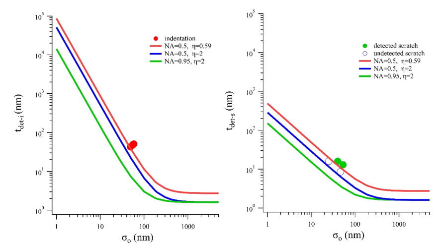
FIG. 3. [(a) and (b)] Detection limits of indentations and scratches in phase-contrast microscopy plotted as functions of the lateral size parameter σ₀ and peak depth t₀. The circles indicate experimental results, while solid lines represent calculated values.
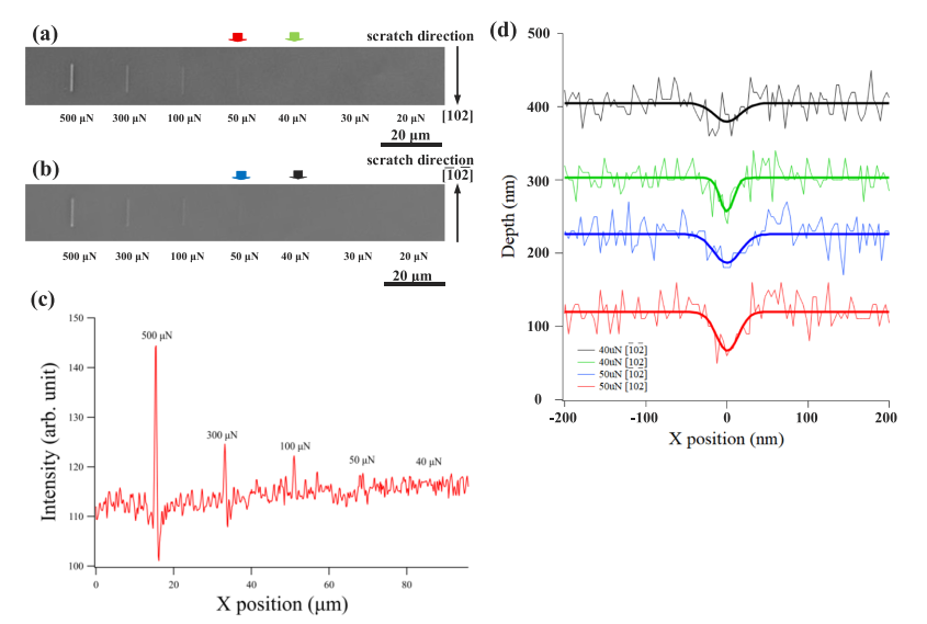
FIG. 4. [(a) and (b)] PCM images of scratches formed by scanning in the upward and downward directions, respectively, as defined in Fig.1 (d). (c) Cross-sectional intensity profile of the scratch shown in (b). (d) Cross-sectional profiles of the AFM image near the center of the scratches, showing the measured profiles (thin lines) and the Gaussian fit (thick lines).
DOI:
doi.org/10.1063/5.0339969
Instruction
Official Account

Cooperation
Top
