


Researchers from the Xi’an Jiaotong University and Xidian University have published a paper titled " High-Performance and Reliability-Enhanced β-Ga2O3 Trench Schottky Barrier Diodes with Ion Implantation Shielding Layer " in 2026 IEEE 38th International Symposium on Power Semiconductor Devices and ICs.
Background
β-Ga₂O₃ exhibits an ultra-wide bandgap of 4.6–4.8 eV and an extremely high critical breakdown field, which endows it with superior Baliga's figure-of-merit and low-cost manufacturing potential for epitaxial layers and substrates compared with SiC and GaN, rendering it a core material for next-generation high-voltage power electronic devices.
Conventional planar Ga₂O₃ Schottky barrier diodes (SBDs) suffer from severe electric field crowding, which increases reverse leakage current and triggers premature breakdown. Trench MOS barrier Schottky (TMBS) diodes adopt fin sidewall MOS capacitors to realize RESURF modulation, shifting peak electric field away from device surface to boost breakdown voltage and suppress leakage. Nevertheless, this structure has inherent drawbacks: dielectric leakage under high reverse bias leads to dielectric-dominated breakdown; MOS interface defects in trenches severely degrade device reliability; in addition, the sidewall MOS structure occupies current conduction paths and raises the specific on-resistance Rₒₙ,ₛₚ greatly.
Previous studies have verified that ion implantation edge termination can form high-resistivity regions around Schottky contacts to mitigate anode-edge electric field crowding, yet this technology only works on planar edges and cannot achieve full electric field shielding on both trench bottoms and sidewalls simultaneously. To address the technical bottleneck that traditional trench TMBS cannot balance conduction loss, breakdown voltage and reliability, this paper proposes a trench Schottky barrier diode (TSBD) with multi-energy nitrogen ion implantation shielding layer.
Abstract
In this paper, a reliable ion-implantation shielded β-Ga₂O₃ trench Schottky barrier diode (TSBD) is demonstrated. By replacing the trench-sidewall MOS capacitor with a multienergy nitrogen ion-implantation layer, the fabricated TSBD eliminates the sidewall depletion effect to expand the current conduction path and lower the specific on-resistance (Rₒₙ,ₛₚ) while also forming a high-resistivity region that shields the Schottky interfaces to mitigate electric field crowding and reverse leakage. The fabricated TSBD achieves a high breakdown voltage (Vᵦᵣ) of 2.77 kV, a low Rₒₙ,ₛₚ of 7.32 mΩ·cm², and a Baliga's figure-of-merit (BFOM) exceeding 1 GW/cm². The robust stability of the TSBD has been comprehensively evaluated for reliability, including high current forward bias stress, off state stress, and multiple thermal cycles up to 600 K, confirmed the robust stability of the device. This work confirms that ion implantation shielding technology is a feasible path for developing high-performance and high reliability β-Ga₂O₃ trench power diodes.
Highlights
A novel β-Ga₂O₃ trench Schottky barrier diode (TSBD) with nitrogen ion implantation shielding layer is proposed. The multi-energy nitrogen ion implantation layer replaces traditional trench sidewall MOS capacitors, eliminates sidewall depletion effect, widens forward current conduction paths and greatly reduces specific on-resistance Rₒₙ,ₛₚ;
Multi-energy nitrogen ion implantation forms high-resistivity shielding regions on both trench bottoms and sidewalls, which comprehensively shield the electric field at Schottky interfaces, suppress electric field crowding, reduce reverse leakage current significantly, realize a breakdown voltage of 2.77 kV and Baliga's figure-of-merit over 1 GW/cm²;
The trench dielectric layer in conventional TMBS structures is removed, eliminating reliability risks induced by dielectric leakage and MOS interface defects;
Multi-dimensional reliability tests including high-current forward bias stress, OFF-state reverse bias stress and multiple thermal cycles up to 600 K are carried out. All device parameter variations are limited within 4%, verifying the long-term stability under high-voltage and high-temperature operating conditions;
The comprehensive performance of the proposed device outperforms all previously reported β-Ga₂O₃ trench TMBS devices, achieving optimal trade-off between breakdown voltage and conduction loss.
Conclusion
In summary, we demonstrate the β-Ga₂O₃ TSBD that utilizes a nitrogen ion-implantation layer for electric field shielding, which can overcome key limitations of conventional TMBS devices, including restricted current path and dielectric reliability. The implanted shielding layer provides a larger conduction area, achieving a low Rₒₙ,ₛₚ of 7.32 mΩ·cm². Meanwhile, it effectively suppresses electric field crowding at critical interfaces,resulting in a high Vᵦᵣ of 2.77 kV and an outstanding BFOM exceeding 1 GW/cm². Robust reliability with minimal performance degradation is demonstrated by extensive reliability tests conducted under forward bias, reverse bias, and high-temperature thermal cycling up to 600 K. This work confirms the strong potential of the proposed TSBD for high-temperature and high-voltage applications.
Project
This work was supported by the Joint Funds of the National Natural Science Foundation of China U23A20367.
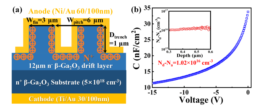
Fig.1. (a) Schematic cross-section of β-Ga₂O₃ TSBD. (b) C-V characteristics. Extracted net doping concentration is 1.02 ×10¹⁶ cm⁻³
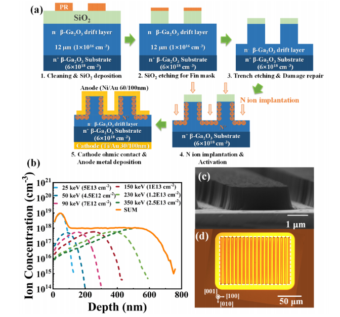
Fig. 2. (a) Main fabrication steps of the TSBD. (b) Simulated N ion profiles in β-Ga₂O₃ by multi-energy implantation. (c) SEM image of the etched trench structure. (d) Optical graph of the top view of the TSBD with an active region area of 100 ×150 μm²
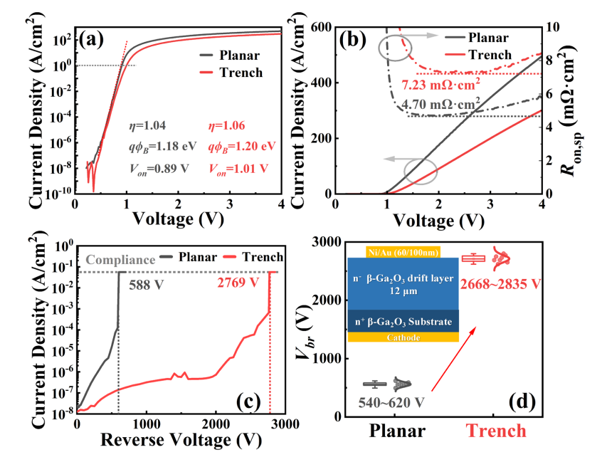
Fig.3. Forward I-V characteristics (a) in semi-log and (b) linear scale of planar and trench SBDs. (c) Breakdown of planar and trench SBDs. (d) Statistical plots of ten device's Vᵦᵣ tested for each structure
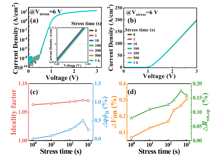
Fig. 4. Forward I-V characteristics of TSBD (a) in semi-log and (b) linear scale after 0-1 ks under 6 V forward-bias stress. (c) η and ΔqϕB, (d) ΔVₒₙ and ΔRₒₙ,ₛₚ as a function of stress time
Fig.5. Forward I-V characteristics of TSBD (a) in semi-log and (b) linear scale after 0-1 ks under -200 V OFF-state stress. (c) η and Δqϕ_B, (d) ΔVₒₙ and ΔRₒₙ,ₛₚ as a function of stress time
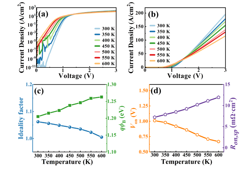
Fig. 6. Temperature-dependent forward I-V characteristics of TSBD (a) in semi-log and (b) linear scale from 300 K to 600 K. (c)η and qϕ_B, (d) the Vₒₙ and Rₒₙ,ₛₚ as a function of temperature
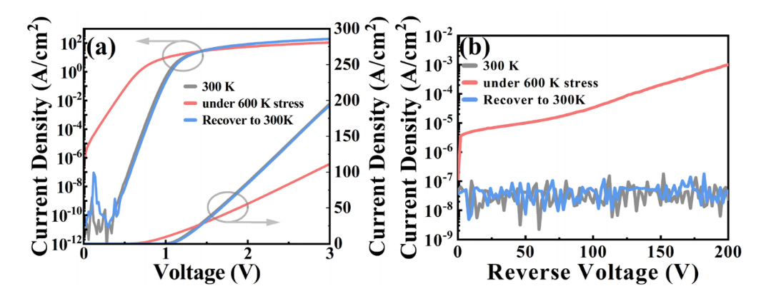
Fig. 7. (a) Forward and (b) reverse I-V curves measured at initial 300K, 600K high-temperature stress for 5 h, and recovery to 300K
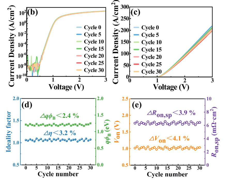
Fig. 8. (a) Schematic diagram of thermal cycling test. Forward I-V characteristics of TSBD (a) in semi-log and (b) linear scale after multiple thermal cycles. (c) η and Δqϕ_B, (d)ΔVₒₙ and ΔRₒₙ,ₛₚ as a function of cycle number
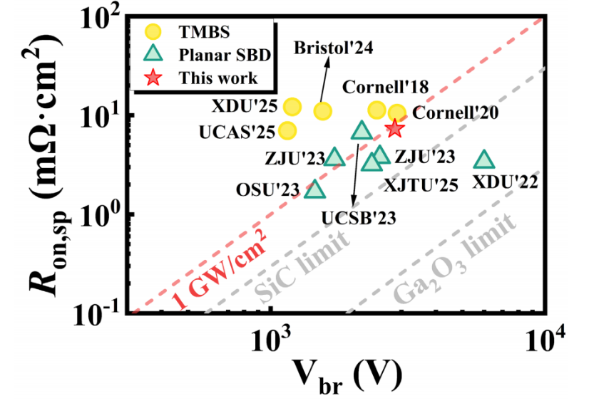
Fig. 9. Benchmark of Rₒₙ,ₛₚ vs Vᵦᵣ of the β-Ga₂O₃ state-of-the-art planar and trench SBDs
DOI :
10.1109/ISPSD64561.2026.11553706
Instruction
Official Account

Cooperation
Top
