


The surface passivation layer of power devices is often regarded simply as the final protective coating added to the device. This understanding may be acceptable for low-voltage devices, but when the blocking voltage rises to hundreds or even thousands of volts, this dielectric layer becomes deeply involved in the electric field distribution of the high-voltage structure. Its quality directly affects terminal breakdown, surface leakage current, threshold voltage stability, and long-term reliability. This series is designed for engineers working in power device fabrication and reliability, as well as students preparing to enter the field. It provides a systematic discussion of passivation stacks — from thermally grown SiO₂ and PECVD Si₃N₄ to top-layer polyimide — covering design constraints, failure mechanisms, and evaluation methods in both active regions and termination regions. The goal is to establish a practical framework for analysis and decision-making, followed by dedicated topics on terminal passivation, packaging interfaces, and failure localization.
Introduction
The dielectric layer on the surface of power devices is generally referred to as the passivation layer. In low-voltage devices, its function is close to its literal meaning: it serves as a protective coating on the top surface of the chip to block moisture and contamination. However, when the blocking voltage rises to hundreds or even thousands of volts, this dielectric layer becomes deeply involved in the electric field distribution of high-voltage structures, and its role extends far beyond that of a simple protective film added at the final stage of fabrication.
The primary materials used in passivation stacks are thermally grown SiO₂ and PECVD Si₃N₄. SiO₂ can form an interface close to ideal on silicon, while on SiC, residual carbon at the interface is difficult to completely eliminate, and on GaN, passivation relies more heavily on deposited dielectric layers. The intrinsic properties of these dielectric materials provide the foundation, but the key focus of this article is the specific roles they perform once integrated into real devices.
During process development, the passivation layer is often treated as a single entity and simply described as a means of “protecting the chip.” However, when applied to IGBTs, power MOSFETs, and fast recovery diodes (FRDs), the same dielectric stack simultaneously performs four physically independent functions under different locations and operating conditions.This article will break down these four functions one by one, provide quantifiable evaluation criteria for each, and establish a clear distinction: the surface of the active region and the termination region represent two fundamentally different challenges and must be addressed separately.
1.One Dielectric Layer, Four Roles
Let us first outline the four roles. The passivation stack on the surface of power devices is typically composed of thermally grown SiO₂, PECVD Si₃N₄, and a top polyimide layer. Together, these layers perform four different functions, and the design goals of these roles often impose competing requirements on one another.
Role 1: Surface-State Passivation Layer
The first role is to suppress semiconductor surface states, interface states, and traps. This involves two levels: the gate oxide or gate dielectric interface adjacent to the channel in the active region, and the dielectric interface on the surface of the termination region. Both rely on interface hydrogen passivation and charge control to reduce trap density, but their locations and failure consequences are different.
At the surface and interface of crystalline silicon, the periodic crystal structure is interrupted, leaving unpaired dangling bonds, commonly referred to as Pb centers. These defects introduce continuously distributed interface states within the bandgap, which are characterized by the interface trap density (Dit), with units of cm⁻²·eV⁻¹. Interface states act both as recombination centers that generate leakage current and as trapping centers that cause threshold voltage shifts. Standard processes use forming gas annealing, typically at around 450 °C, introducing hydrogen through N₂/H₂ or Ar/H₂ atmospheres. The hydrogen bonds with dangling bonds, significantly reducing electrically active interface states.
The key evaluation parameter is Dit. An optimized process combining dry oxygen thermal oxidation with forming gas annealing can reduce the Dit at the Si(100)/SiO₂ interface to the order of 10¹⁰ cm⁻²·eV⁻¹. In contrast, untreated directly deposited oxides typically remain around 10¹² cm⁻²·eV⁻¹, representing a difference of approximately two orders of magnitude. Fixed oxide charges (Qf) are concentrated within about 2 nm of the interface and are predominantly positive charges. The (111) crystal plane typically exhibits a Qf level about three times higher than that of the (100) plane. An increase in interface states manifests as higher peripheral leakage current and degraded threshold voltage stability.
Role 2: Electric Field Modulation Layer
The second role emerges in the termination region, beneath field plates, and around the gate-drain region. The thickness, dielectric constant, and fixed charge of the passivation layer can directly reshape the electric field distribution at the semiconductor surface.
The underlying mechanism comes from the continuity of electric displacement. When there is no charge at the interface, the normal component of electric displacement remains continuous, and the electric field in the dielectric is equal to the electric field in silicon multiplied by the ratio of their dielectric constants. Taking the relative permittivity of silicon (11.7) as a reference, SiO₂ has a value of approximately 3.9, resulting in an electric field amplification of about 3.0 times within the dielectric; Si₃N₄ has a value of approximately 7.5, resulting in an amplification of about 1.6 times. The effectiveness of a field plate also depends on the dielectric breakdown strength, fixed charge, and edge geometry. The dielectric constant is only one factor: a higher dielectric constant can enhance electrostatic coupling, but may also introduce additional challenges such as fixed charges and mechanical stress.
The influence of fixed charges is equally direct. Silicon has a characteristic breakdown charge scale on the order of 10¹² cm⁻², which can be understood as the product of silicon permittivity and critical electric field divided by the elementary charge. Taking the critical electric field as approximately 2–3×10⁵ V/cm gives a value in the range of 1–2×10¹² cm⁻². This value varies with doping concentration and critical electric field, and is not an intrinsic constant of the material. Once the surface charge in the termination region approaches a significant fraction of this level, the edge electric field balance is modified, causing fluctuations in the terminal breakdown voltage.
Role 3: Barrier Layer
The third role is to block external contamination. Alkali metal ions such as Na⁺ and K⁺ exist as small-radius positive ions in SiO₂. Even under moderate electric fields at room temperature, they can drift through the thermal oxide layer and migrate toward the interface, causing threshold voltage shifts and increased leakage current. Moisture, meanwhile, can penetrate into the termination region through defects, interfaces, and edge pathways. Under high temperature, high humidity, and high electric field conditions, it increases surface conductivity and triggers ion migration and electrochemical corrosion. Dense PECVD Si₃N₄ contains almost no pathways for such migration and therefore serves as an excellent barrier layer; PSG and BPSG rely on phosphorus to capture Na⁺ ions.
An important engineering consideration should be added here: actual failures rarely result from moisture uniformly permeating through an intact thin film. Instead, moisture and contaminants typically enter through pinholes, microcracks, weak step coverage regions, metal edges, bond pad openings, and dicing edges. Weak points are concentrated around openings, edges, and steps, while flat regions are relatively safer. This role becomes particularly critical during reliability evaluations such as HTRB, H3TRB, and THB.
Role 4: Mechanical Protection Layer
The fourth role is to withstand mechanical and thermal stresses, including packaging stress, temperature cycling, dicing-edge damage, thick metal stress, and moisture-induced swelling of organic materials. PECVD Si₃N₄ contains a relatively high amount of hydrogen, and its stress state varies with the SiH₄, NH₃, and N₂ gas ratios, RF power, deposition temperature, and post-treatment conditions. It can exhibit either compressive or tensile stress. Dehydrogenation treatments such as UV curing can shift the film toward tensile stress, with stress levels reaching approximately 1.6 GPa. To improve barrier performance, the film is often made denser; however, densification is typically accompanied by increased stress and a higher risk of cracking.
Polyimide has a much lower elastic modulus than inorganic Si₃N₄ and can absorb strain energy from packaging and temperature cycling through relatively large elastic and plastic deformation. Therefore, it is suitable as a buffer layer placed on the top of the passivation stack. When a dicing blade cuts through brittle silicon, it can leave chipping damage of approximately 2–3 μm along the active-side edge of the cut surface, while the backside edge may exhibit larger chipping ranging from 10–100 μm. Such damage can also propagate along the scribe line toward the active device region.
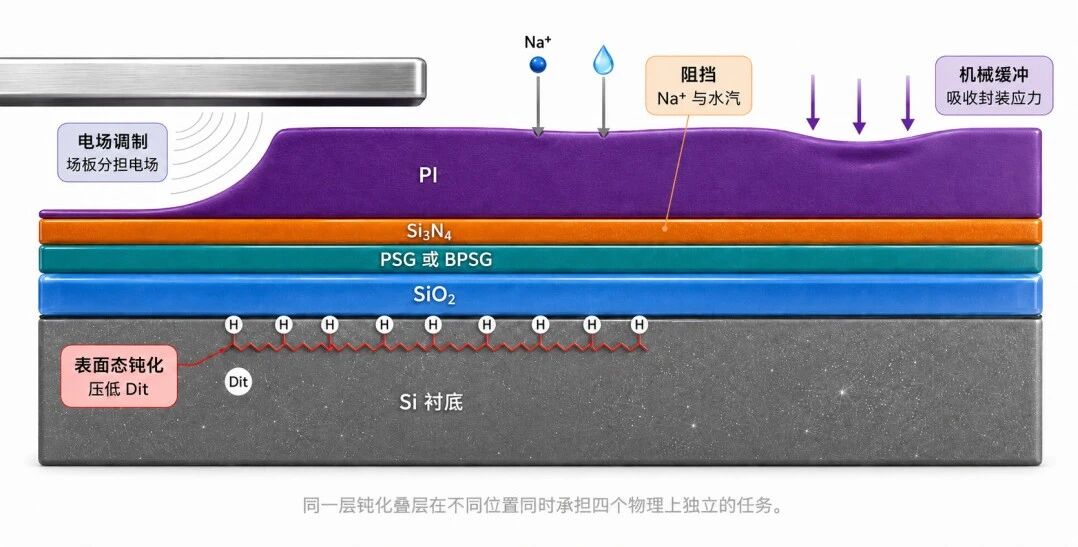
Figure 1. Four Roles of a Single Dielectric Layer
2.A Critical Boundary: The Active Region Surface and the Termination Region
After clarifying the four roles, an even more important dividing line must be established. The surface of the entire chip can be divided into two fundamentally different engineering domains, each with distinct failure mechanisms, design constraints, and dielectric requirements. Treating them as the same problem is one of the most common mistakes in passivation design.
Active Region: Interface Quality and Gate Oxide Reliability
The active region is where the main current flows, including the cell array and gate region. The interface directly adjacent to the channel, which determines Dit and Qf, is the gate oxide or gate dielectric interface. The top passivation layer is separated from the channel by multiple dielectric layers and primarily serves as a barrier and mechanical protection layer in the active region.
On the channel side, the primary task is to control the quality and long-term reliability of the gate oxide interface. Failure manifestations include threshold voltage shift, degradation of transconductance and carrier mobility, gate leakage current, and bias temperature instability (BTI) under high-temperature gate bias conditions. The key design constraints are low Dit, low concentration of mobile ions, and stable gate dielectric properties, with high-temperature gate bias (HTGB) as the corresponding reliability test.
Termination Region: Electric Field Reshaping and Humidity Stability
The termination region does not carry the main current, but it must withstand the entire blocking voltage at the device periphery. Junctions formed by planar processes exhibit cylindrical or spherical geometries at the edge, with curvature radii approximately equal to the junction depth. Electric fields become strongly concentrated at these edges: the larger the curvature effect, the more densely the equipotential lines are compressed, resulting in higher electric fields and making breakdown likely to occur first at the edge.
A classic example illustrates this effect. For an abrupt silicon junction with a doping concentration of 10¹⁵ cm⁻³, the ideal parallel-plane junction has a breakdown voltage of approximately 330 V. However, this decreases to about 80 V at a cylindrical edge with a junction depth of 1 μm, and further drops to only around 39 V for a spherical geometry. This explains why devices without termination structures can achieve only 10–30% of the ideal breakdown voltage, while optimized termination designs can recover the value to more than 90%.
The primary tasks of the termination region are to reshape the electric field, suppress surface conduction channels, and block external charges and moisture. Design constraints focus on precise control of dielectric thickness, dielectric constant, and fixed charge. Failure manifestations include degradation of terminal breakdown voltage, increased surface leakage current, and humidity-related failures during H3TRB and high-voltage temperature humidity bias (HV-THB) testing.
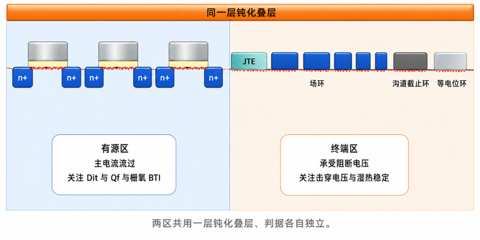
Figure 2. Boundary Between the Active Region and the Termination Region
3.Mapping the Four Roles onto the Two Regions
The engineering logic becomes complete only when the four roles are considered together with the two regions, because the importance of each role differs between the two areas. Surface-state passivation dominates in the active region, where the channel directly resides at the interface. Dit directly translates into changes in carrier mobility and threshold voltage stability. In the termination region, its influence is reduced, but surface states can still induce inversion or accumulation layers, creating surface leakage paths. Electric field modulation, on the other hand, is primarily important in the termination region. Field plates rely on dielectric and surface coupling to spread out the peak electric field at the edge of the main junction, with the effect determined by the thickness, dielectric constant, and fixed charge of the field oxide.
Barrier protection is required in both regions, but it is particularly critical in the termination region. Once moisture and mobile ions enter the high-field termination area, leakage increases and breakdown degradation occur more rapidly. Mechanical protection covers the entire chip, but the main challenges are concentrated at chip edges and around thick metal structures. Dicing chipping, thick metal stress, and thermal expansion mismatch between molding compounds and silicon all become most apparent at the edges. Bond pad openings, thick aluminum edges, field plate edges, and scribe lines are often common locations for moisture ingress, crack initiation, and electric field concentration. Therefore, the coverage quality of the passivation stack at these locations often has a greater impact on long-term reliability than that in flat regions.
4.Typical Passivation Stack: Division of Roles Among the Four Functions
The four roles are difficult to fulfill with a single material because the optimal solutions often conflict with one another. Si₃N₄, with its high dielectric constant, is beneficial for electric field modulation and barrier protection, but it also has high tensile stress and is prone to cracking. Polyimide, while an excellent stress-buffering layer, is inherently moisture-absorbing and does not provide strong water-blocking capability. The engineering solution is a functionally divided multilayer stack, where each layer primarily performs the role it is best suited for. A typical passivation stack for silicon power devices consists of four layers from bottom to top, with each layer dominating one or two specific functions.
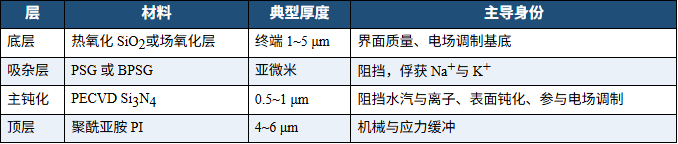
The choice of film material for each layer in the stack is determined by the function it needs to perform. The same Si₃N₄ material can play different roles depending on its position within the structure. It should also be emphasized that the chip-level passivation stack is only the starting point of the packaging interface. Humidity-related failures are rarely determined by a single dielectric layer alone. Instead, they are typically governed by the combined effects of the chip passivation layer, defects at openings and step edges, polyimide or PBO layers, silicone gels, and molding compounds. Optimizing the chip-level passivation layer does not eliminate all reliability challenges; rather, it transfers the remaining challenges to the package interface.
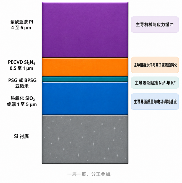
Figure 3 Typical Passivation Stack and the Primary Roles of Each Layer
5.Four Roles, Four Types of Reliability Stress Testing
Each of the four roles corresponds to different reliability stress tests. This mapping relationship provides the foundation of the evaluation framework: during design, evaluation criteria are assigned according to each role; during verification, appropriate tests are selected based on the role being assessed; and during failure analysis, root causes are traced back according to the specific role involved. The table below summarizes the correspondence between the four roles and commonly used reliability tests. Specific test conditions should follow the requirements of JEDEC, AEC-Q101, AQG-324, or customer and company specifications.
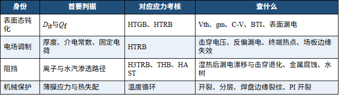
This table should be interpreted both horizontally and vertically. Horizontally, each role is linked to a specific evaluation parameter, a category of reliability testing, and a corresponding set of failure phenomena. Vertically, it can be used as a diagnostic tool: for example, if a device passes all room-temperature tests but exhibits a sharp increase in leakage current after H3TRB testing, the issue is most likely located at the intersection between the barrier function and the termination region.
6.The Evaluation Framework of This Article
At this point, the overall framework is built upon two pillars. The first pillar consists of the four roles: surface-state passivation, electric field modulation, barrier protection, and mechanical protection. Although they are fulfilled by the same passivation stack, each role is evaluated according to a different set of criteria. The second pillar consists of the two regions: the active region surface and the termination region. They involve different physical mechanisms and require different dielectric design considerations, and therefore must be addressed separately.
Nearly every process choice and failure phenomenon associated with passivation layers can be mapped to one specific point at the intersection of these four roles and two regions. With this coordinate system in hand, the analysis of specific problems becomes much clearer: achieving good dielectric properties alone does not necessarily guarantee device reliability. Whether the device can remain stable under the combined stresses of high voltage, humidity, temperature, and mechanical stress ultimately depends on whether these four roles can simultaneously perform effectively in both regions.
Instruction
Official Account

Cooperation
Top
