


Recently, the national standard “Measurement of Carrier Concentration in Gallium Oxide Epitaxial Layers — Capacitance-Voltage Method,” led by Hangzhou Fujia Gallium Technology Co., Ltd., has completed the project approval announcement. This marks the second national standard in the gallium oxide field led by Fujia Gallium, following its leadership in drafting the first national standard for gallium oxide, “Gallium Oxide Single-Crystal Polished Wafers.” The achievement further demonstrates Fujia Gallium’s commitment and responsibility in driving the standardized and large-scale development of the industry through technological innovation and standardization efforts, while supporting the independent advancement and upgrading of China’s ultra-wide-bandgap semiconductor industrial chain.
National Standards: The "Baseline" for Industrial Development
National standards are technical specifications approved and issued by the Standardization Administration of China (SAC) and uniformly applied nationwide. They represent the highest level of authority and regulatory guidance among technical standards, serving as a common technical basis for enterprise production, quality inspection, market access, and trade activities. The establishment of a national standard often indicates that a technological field has entered a stage of large-scale and standardized development. It plays a profound role in guiding industrial investment directions, ensuring product quality, and facilitating international alignment.
National Standards Leading the Way: Accelerating the Industrialization of Gallium Oxide
As a core material for fourth-generation semiconductors, gallium oxide features a theoretical breakdown electric field of up to 8 MV/cm, offering significant advantages in high-voltage and high-power devices. It is widely regarded as a key direction for next-generation power electronics technologies. However, during the industrialization process, the industry faces a common challenge: inconsistent testing methods for material parameters among different organizations, making data difficult to compare and increasing the technical coordination costs between upstream and downstream enterprises, which significantly limits the efficiency of industrial chain collaboration. The establishment of national standards provides a critical solution to this bottleneck. Unified testing methodologies will enable substrate manufacturers, epitaxial material producers, and device companies to adopt a common technical language, greatly reducing communication costs across the industrial chain and laying a solid foundation for the large-scale production of gallium oxide devices.
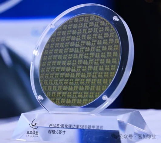
Filling the Gap in Epitaxial Layer Testing Methods and Building a Comprehensive Standard System
Carrier concentration is one of the most critical electrical parameters of gallium oxide epitaxial wafers, directly determining the voltage withstand capability and conduction performance of power devices. The capacitance-voltage (C-V) method is currently one of the most accurate approaches for measuring carrier concentration profiles in semiconductor epitaxial layers. However, the unique physical properties of gallium oxide impose more stringent requirements on testing conditions and data processing procedures. The establishment of this standard will provide an authoritative and unified technical basis for the quality evaluation of gallium oxide epitaxial wafers.
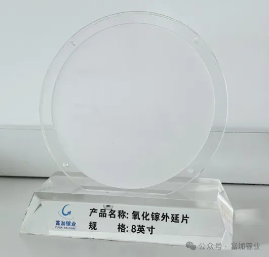
Together with the previously approved national standard project “Gallium Oxide Single-Crystal Polished Wafers,” Fujia Gallium is simultaneously advancing the development of two national standards, jointly establishing a comprehensive gallium oxide material standard system covering the entire “substrate–epitaxy” value chain. Fujia Gallium will continue to focus on gallium oxide material technologies, lead industrial development through standardization, uphold its mission of “providing the world with high-quality materials,” and contribute to the high-quality growth of the fourth-generation semiconductor industry.
Further Reading: The Importance of Standards
Within the standardization system, national standards (GB/T) and group standards (T/) are two common forms. They differ fundamentally in terms of their drafting bodies, scope of application, and authority, and they have different impacts on industrial development.
In terms of drafting bodies and scope of application, national standards are uniformly approved and issued by the Standardization Administration of China (SAC) and have nationwide applicability. They serve as authoritative references in scenarios such as government procurement, market access, and judicial appraisal. Group standards, on the other hand, are developed by social organizations such as academic societies, industry associations, or industrial alliances. Their application is generally limited to members of the relevant organizations, and their recognition may vary in broader market environments.
Regarding development cycles, national standards must go through rigorous procedures including project approval announcements, drafting, public consultation, technical review, and official approval and release. The entire process typically takes 2–5 years, with each stage subject to review and oversight by relevant authorities. The process for developing group standards is relatively more flexible, generally taking 1–2 years. In emerging fields, however, differences in standard quality may sometimes occur.
In terms of industry status, national standards serve as the “anchor” that ensures safety and maintains fundamental requirements, while group standards, driven by market demand, act as an “innovation accelerator” that enables rapid responses to emerging needs. Once issued, a national standard becomes a technical benchmark jointly followed by the entire industry, playing an important role in unifying technical communication across the industrial chain, regulating market order, and promoting international recognition and mutual acceptance.
Therefore, taking the lead in developing a national standard not only represents recognition of an enterprise’s technological capabilities at the national level, but also demonstrates its sense of responsibility in fulfilling its mission and serving the industry. Fujia Gallium’s leadership in drafting its second national standard for gallium oxide marks a critical step toward establishing unified industry-wide standards for gallium oxide epitaxial layer testing methods.
Product Portfolio
Gallium Oxide Crystal Growth Equipment
Fujia Gallium has developed the world’s first EFG crystal growth system featuring a proprietary “one-click crystal growth” function, supporting 2-inch to 8-inch crystal production. The system is protected by 6 granted domestic patents and 4 international patents. Complete equipment solutions and process packages are available. The company has also independently developed fully automated VB (Vertical Bridgman) crystal growth equipment and was the first in China to overcome the technical bottleneck of 12-inch Ga₂O₃ single-crystal growth using the VB method, enabling the production of large-diameter bulk crystals. Currently, this equipment has been granted 6 domestic patents and 4 international patents, and VB systems along with process packages can be provided based on customer requirements.
Gallium Oxide Single-Crystal Substrates
As one of China’s earliest pioneers in Gallium Oxide single-crystal research and an industry-leading supplier, Fujia Gallium provides high-quality single-crystal substrates to global customers. The product portfolio includes 26 standard Ga₂O₃ substrate specifications covering diameters from 2 to 8 inches. Customized solutions are available in terms of wafer size, electrical properties, and crystal orientation, supporting both advanced epitaxy R&D and volume production requirements.
Gallium Oxide Epitaxial Wafers
Built upon mature MOCVD (Metal-Organic Chemical Vapor Deposition) and MBE (Molecular Beam Epitaxy) platforms, Fujia Gallium offers 15 standard epitaxial wafer products from 2-inch to 6-inch formats, as well as customized MBE-based epitaxial structures. The company provides integrated “substrate + epitaxy” solutions. A precise process control system enables customization of key parameters including epitaxial layer thickness, doping concentration, and compositional uniformity, meeting diverse requirements across different power levels and device architectures.
About Hangzhou Fujia Gallium
Hangzhou Fujia Gallium Technology Co., Ltd., established on December 31, 2019, is committed to its mission of “Bringing Better Materials to the World” and focuses on the industrialization of ultra-wide bandgap Gallium Oxide semiconductor materials. Its core products include Gallium Oxide single-crystal substrates, MOCVD/MBE epitaxial wafers, and crystal growth equipment based on the Vertical Bridgman (VB) and Edge-Defined Film-Fed Growth (EFG) methods. The company provides systematic solutions for material development, accelerating the integration of the entire ultra-wide bandgap Gallium Oxide industry chain and promoting the application of Gallium Oxide materials in power devices, microwave RF devices, and optoelectronic detection. A series of major achievements in Gallium Oxide development have been featured by leading media outlets including CCTV, People’s Daily, Xinhua News Agency, China Securities Journal, and The Paper. In terms of corporate recognition, the company was designated as a Zhejiang Province Science and Technology SME in 2022, recognized as a National High-Tech Enterprise in 2023, and awarded the titles of Hangzhou High-Tech Enterprise R&D Center and Zhejiang “Specialized and Sophisticated” SME in 2024. In 2025, it obtained ISO 9001 Quality Management System certification (Certificate No. 20225Q20294R0M) and was also named a 2024 Hangzhou “Rising Eagle” Enterprise. In the Gallium Oxide field, the company is leading the drafting of the first national standard in this area and has undertaken one project from the National Development and Reform Commission and one from the Ministry of Industry and Information Technology, while participating in three additional national and provincial-level projects supported by the National Natural Science Foundation of China and regional authorities in Zhejiang and Shanghai. To date, the company has been granted 14 international patents (6 in the United States, 7 in Japan, and 1 in Europe), 42 domestic patents, three registered “Fujia Gallium” trademarks, and five software copyrights, including its proprietary “One-Click Crystal Growth” control software.
Instruction
Official Account

Cooperation
Top
