


Researchers from the Nanjing University of Posts and Telecommunications have published a dissertation titled " Doping and Defect Co-Engineering Strategy to Overcome Gain-Speed Dilemma of Ga2O3 Thin Film Grown by Mist-CVD Technique " in Journal of Materials Chemistry C.
Background
With the rapid iteration of new-generation electronic systems such as artificial intelligence, high-reliability power electronics, and solar-blind ultraviolet photodetection, the requirements of devices for low power consumption, ultra-fast response, high photoelectric gain, high breakdown voltage, and extreme environmental resistance are continuously surging. Ultra-wide bandgap (UWBG) semiconductors have become core candidate materials for next-generation high-performance optoelectronic and power devices due to their ultra-large bandgap, high critical breakdown electric field, and excellent chemical and thermal stability, including AlN, diamond, gallium oxide (Ga₂O₃), etc. Among them, α-Ga₂O₃ can be epitaxially grown on sapphire substrates via mist chemical vapor deposition (Mist-CVD). It shares the same corundum crystal system with sapphire, exhibiting crystal quality close to single-crystal β-Ga₂O₃. Meanwhile, it possesses a wider bandgap and shorter solar-blind cut-off wavelength. Besides, Mist-CVD features vacuum-free, low-cost and large-area fabrication, making it highly promising for ultraviolet photodetectors.
UWBG semiconductors generally face obstacles in controllable doping: the wide bandgap, complex crystal structures and deep impurity levels lead to high doping activation energy, low carrier mobility and poor doping efficiency. The doping regulation of Ga₂O₃ encounters more severe contradictions. In existing studies on tin-doped gallium oxide, divalent tin (Sn²⁺) easily forms deep acceptors and carrier recombination centers, which greatly shorten the lifetime of photogenerated carriers and improve device response speed, yet drastically degrade electrical conductivity and photoelectric gain. Tetravalent tin (Sn⁴⁺) acts as shallow donors to realize n-type conductivity and boost device gain, but it tends to generate deep DX trap states that capture photogenerated carriers and prolong relaxation time, resulting in an inherent trade-off between gain and response speed, namely the gain-speed dilemma.
Current strategies to alleviate this trade-off mainly focus on device microstructure design (nanowires, heterojunctions, nanorods). Researches interpreting the physical mechanism of gain-speed contradiction from the perspective of intrinsic material doping and defect co-regulation are extremely scarce. During Mist-CVD growth of Sn-doped α-Ga₂O₃, the oxidation equilibrium of SnCl₂ precursor strongly depends on the hydrogen ion concentration of the system. Hydrochloric acid (HCl) concentration can modulate the valence distribution of Sn²⁺/Sn⁴⁺, lattice defects, crystal quality and electrical transport properties in thin films. Accordingly, this work adjusts Sn valence and defect evolution via variable HCl concentrations, and systematically reveals the internal physical mechanism of doping-defect co-engineering to overcome the gain-speed dilemma of Ga₂O₃.
Abstract
Aiming at the severe challenges of hard controllable doping in ultra-wide bandgap Ga₂O₃ and the inherent gain-response speed trade-off of solar-blind ultraviolet photodetectors, this work takes tin-doped α-Ga₂O₃ thin films grown via mist chemical vapor deposition (mist-CVD) as the research object, and proposes a novel strategy to co-regulate Sn valence states and film defects by adjusting the hydrochloric acid concentration in precursor solutions. A series of thin films are fabricated with gradient HCl contents, and multiple characterizations including XRD, SEM, TEM, XPS, Hall measurement, UV-vis absorption spectroscopy and dynamic UVC photoresponse tests are carried out to explore the evolution of crystallinity, lattice defects, Sn²⁺/Sn⁴⁺ ratio, electrical conductivity, optical bandgap and photodetection performance against acidity. Combined with growth chemical reactions, Mott metal-insulator transition, DX deep trap states and persistent photoconductivity effect, the microscopic mechanism of gain-speed dilemma originated from the competition between Sn²⁺ recombination centers and Sn⁴⁺ donors/traps is clarified from the perspective of material physics. The optimal acidity window is identified, and the essential reason for low Sn doping activation efficiency is analyzed. This work provides theoretical guidance and growth process for Ga₂O₃ optoelectronic devices with both high gain and fast response without complex microstructure modification.
Highlights
A novel doping and defect co-engineering strategy via tuning HCl concentration in precursor solution is proposed for mist-CVD grown Sn-doped α-Ga₂O₃. The ratio of Sn²⁺/Sn⁴⁺, crystallinity, intrinsic defects and electrical transport properties can be precisely modulated only by adjusting hydrochloric acid content, realizing flexible trade-off regulation between photoconductive gain and response speed without complex device microstructure modification.
The microscopic physical origin of the inherent gain-speed dilemma in ultra-wide bandgap Ga₂O₃is fully revealed from the perspective of material physics: substitutional Sn⁴⁺ shallow donors boost carrier concentration and photoelectric gain, yet generate deep DX trap states that prolong carrier lifetime and slow down photoresponse; Sn²⁺ acts as deep acceptors and recombination centers to accelerate the recombination of photogenerated electron-hole pairs and improve response speed, while sacrificing electrical conductivity and photoconductive gain, resulting in intrinsic performance trade-off induced by coexisting Sn valence states.
The optimal acidity window of precursor solution for mist-CVD Sn:α-Ga₂O₃thin films is identified. The optimized sample achieves outstanding n-type conductivity with conductivity of 2 S·cm⁻¹, carrier concentration of 2.1×10¹⁸ cm⁻³ and electron mobility of 6.23 cm²·V⁻¹·s⁻¹, accompanied by greatly improved crystalline quality with XRC FWHM down to 150 arcsec. The core reason for extremely low Sn doping activation efficiency is quantitatively clarified as carrier compensation caused by DX deep traps.
Schematic diagrams of crystal structure and band evolution under different precursor acidities are established. The microscopic mechanism that in-plane compressive strain in sapphire/α-Ga₂O₃heteroepitaxial system stabilizes DX states and SnGa-VGa vacancy complexes induce persistent photoconductivity (PPC) is elucidated, offering universal theoretical guidance for doping and defect regulation of ultra-wide bandgap semiconductors.
Different from conventional device geometry optimization methods, this work opens up a brand-new route of precursor doping-defect co-modulation, providing a facile material growth strategy for next-generation solar-blind ultraviolet photodetectors and power electronic devices that simultaneously require high gain and ultra-fast response speed.
Conclusion
In summary, the properties of Sn:α Ga₂O₃ films are effectively modulated by precisely adjusting the HCl concentration in the mist CVD precursor solution, thereby directly impacting the films' crystallinity, chemical composition, and optoelectronic performance. An optimal HCl concentration range has been successfully identified where the maximum incorporation of desirable substitutional Sn(IV) donors is achieved, Within this specific window, the material exhibits outstanding n -type conductivity (σ=2 S·cm⁻¹) a strong carrier concentration (n=2.1 ×10¹⁸ cm⁻³), and considerable mobility (μₙ=6.23 cm²/V/s), and the crystallinity of the deposited film is improved (XRC FWHM=150 arcsec). However, the presence of DX states at this optimal concentration limits activation efficiency and caps the maximum potential gain achievable in high-performance electronic devices, while excessively high or low acidity introduces deep acceptor defects (Sn²⁺ states) that sacrifice conductivity for increased device speed. These results explain the fundamental "gain-speed dilemma" in UWBG semiconductors from a material physics perspective, underscoring the urgent need for further innovations in material science to overcome these fundamental trade-offs and meet the demanding requirements of next-generation highgain and ultra-fast electronic systems.
Project
This work was supported by the National Natural Science Foundation of China (Grant No. U23A20349, 62305171, 62204125, 62564011, 62501320), the Program of China Scholarship Council (Grant No. 202508320243), the Key Technology Project of Suzhou City (Grant No. SYG2024003), the Jiangsu Provincial Team of Innovation and Entrepreneurship (Grant No. JSSCTD202351), the Fundamental Research Program of Shanxi Province (Grant No. 202103021223388), the Steed Plan of Inner Mongolia University for Introducing High-Level Talents (Grant Nos. 10000-A24199006 and 10000-A24106015), the Inner Mongolia University Experimental Technology Research Project in 2025 (Self-Made and Modified Equipment Project) (Grant No. SYJS2025004), the Inner Mongolia Autonomous Region-level Scientific Research Fund for HighLevel Talents (Grant Nos. 21700-252904 and 21700-252905), and the Program for Innovative Research Team in Universities of Inner Mongolia Autonomous Region (Grant No. NMGIRT2503).
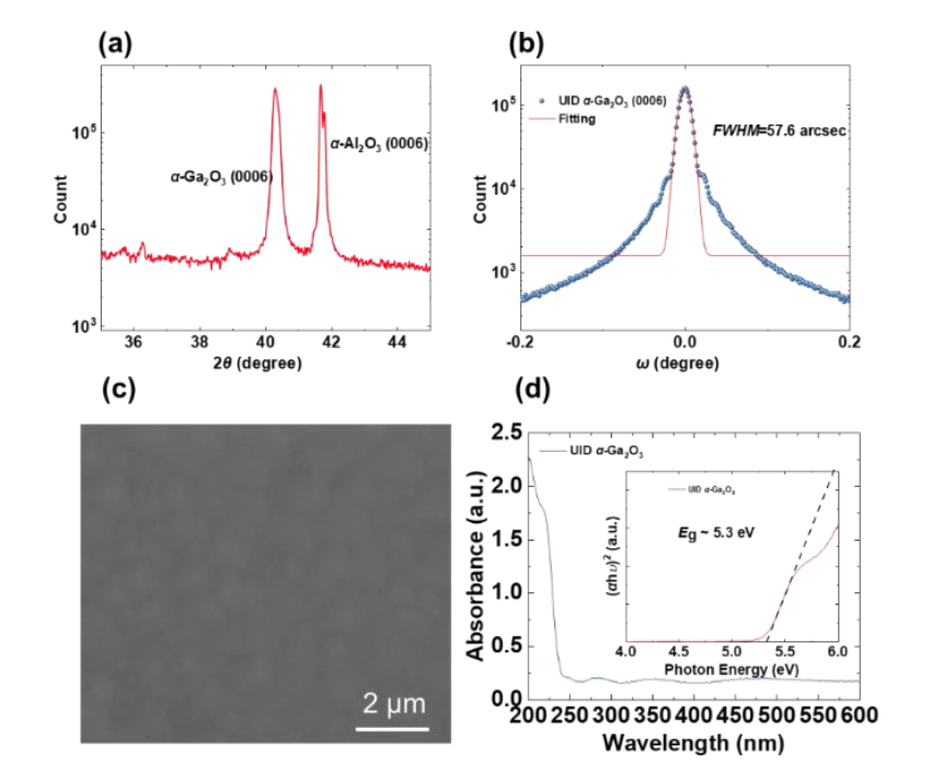
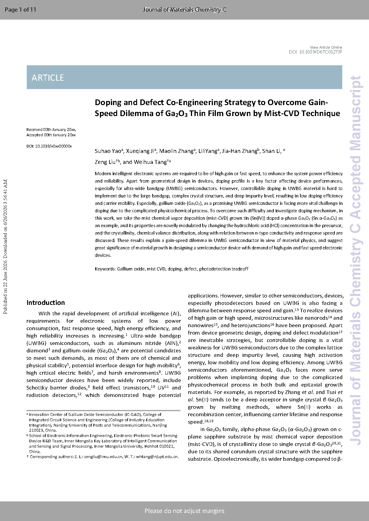
Fig. 1. (a) XRD 2θ/θ spectrum of the deposited UID α-Ga₂O₃, (b) XRD ω-scan of UID α-Ga₂O₃ (0006) peak, (c) surface SEM photograph, and (d) absorbance spectrum and Tauc’s plot of the deposited UID α-Ga₂O₃
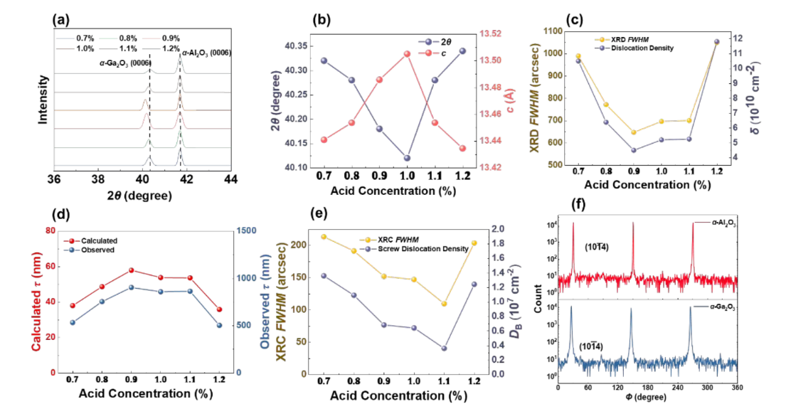
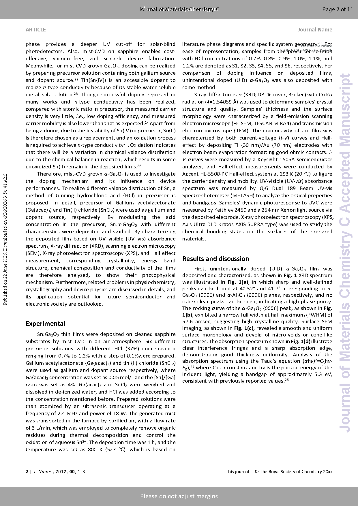
Fig. 2. (a) XRD pattern, (b) Bragg angle θ and lattice constant c, (c) FWHM of the α-Ga₂O₃ peak in XRD and dislocation density δ calculated and witnessed grain size r of the deposited film. (e) XRD Φ -scan measurement for the (10-14) plane of the α-Al₂O₃ (upper) and α-Ga₂O₃ (lower) substrate. (f) FWHM of the α-Ga₂O₃ peak in XRC and screw dislocation density DB in each sample
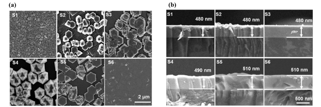
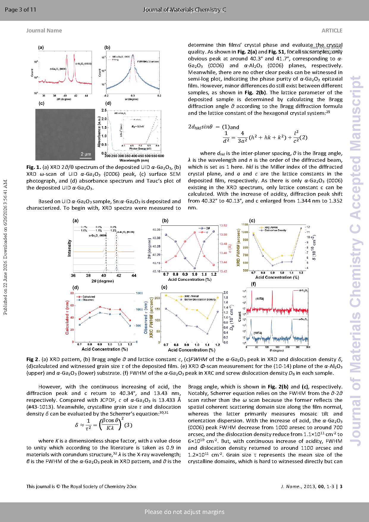
Fig 3. (a) surface and (b) cross-section photograph of the deposited thin film
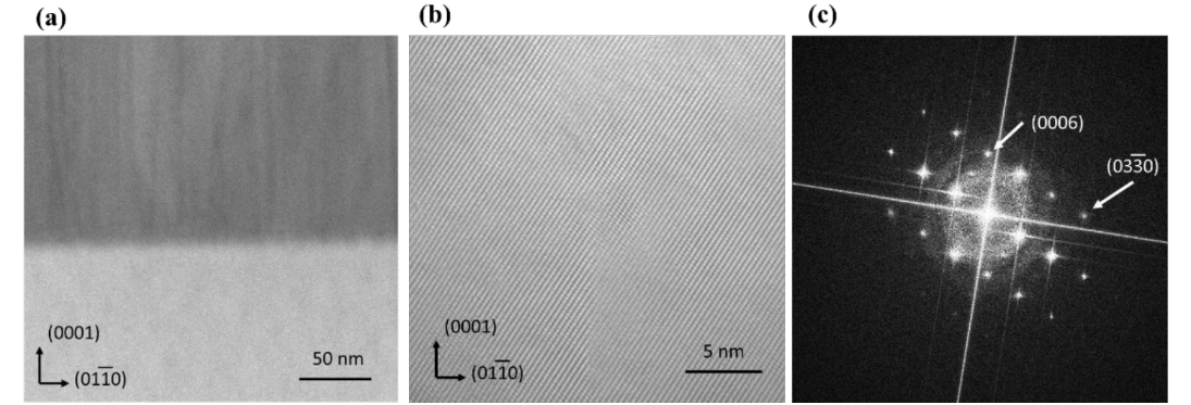
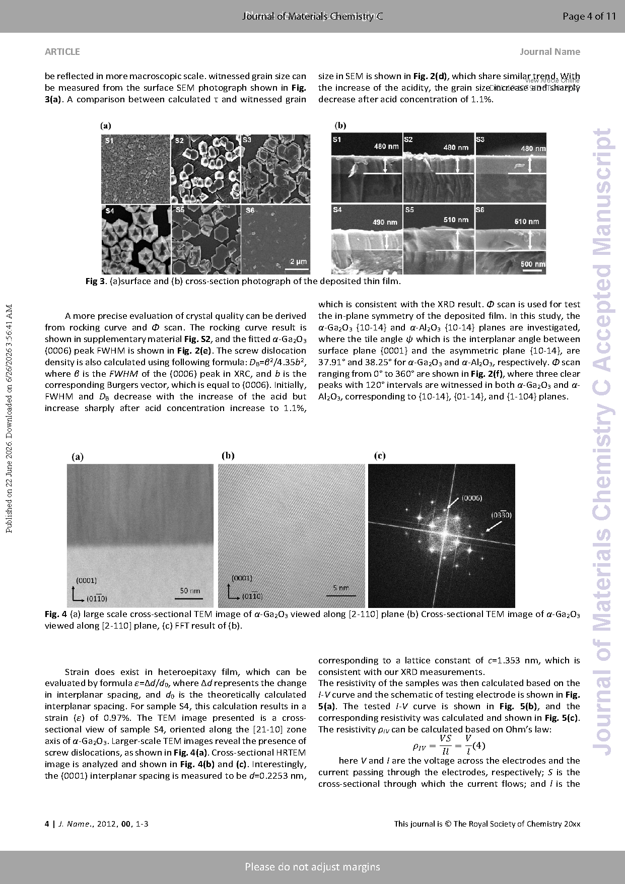
Fig. 4 (a) large scale cross-sectional TEM image of α-Ga₂O₃ viewed along [2-110] plane (b) Cross-sectional TEM image of α-Ga₂O₃ viewed along [2-110] plane, (c) FFT result of (b)
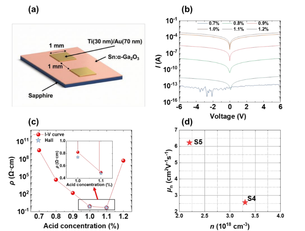
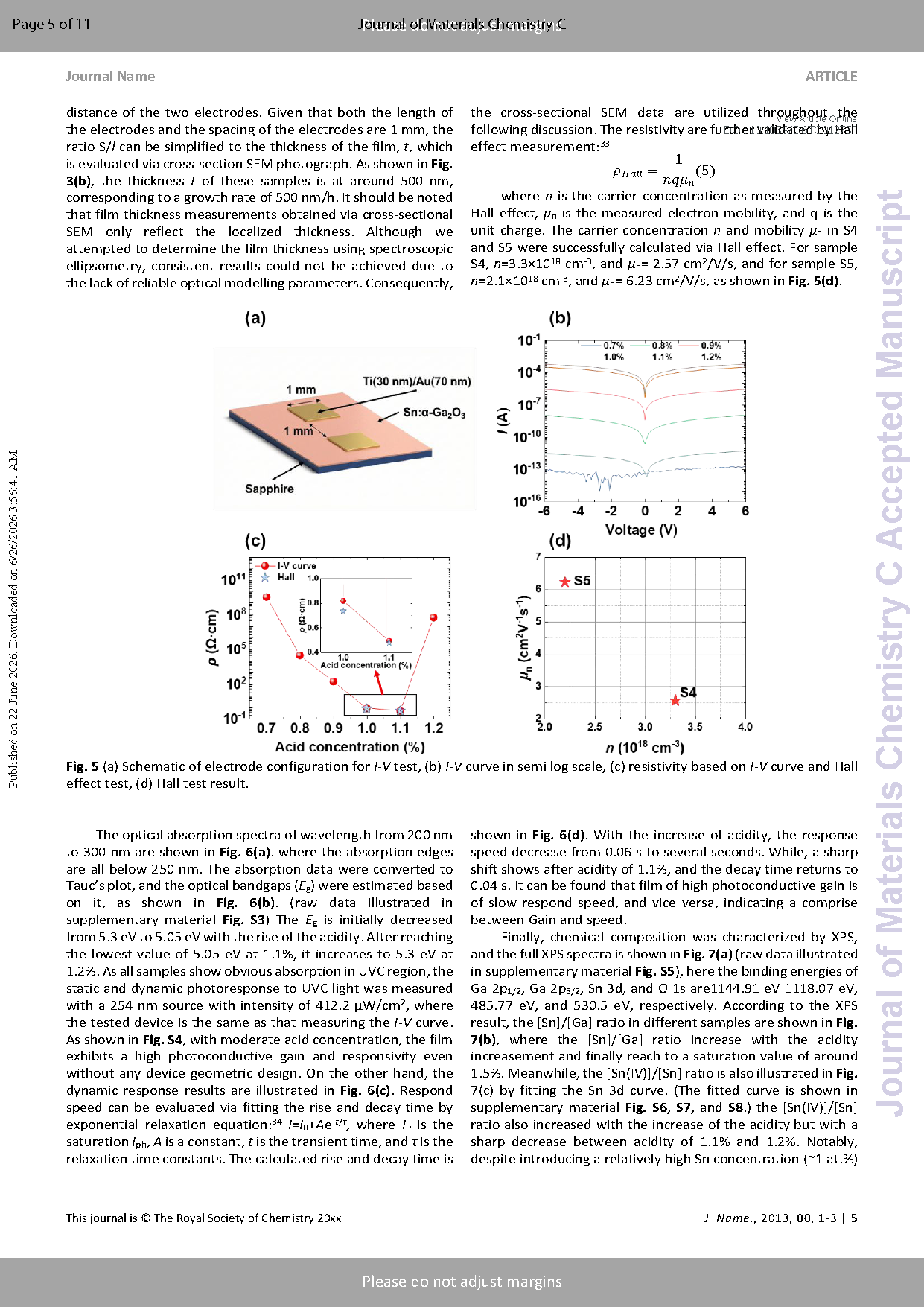
Fig. 5 (a) Schematic of electrode configuration for I-V test, (b) I-V curve in semi log scale, (c) resistivity based on I-V curve and Hall effect test, (d) Hall test result
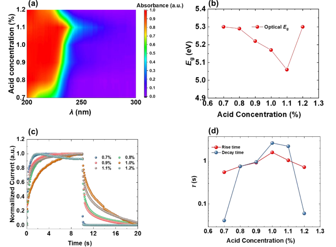
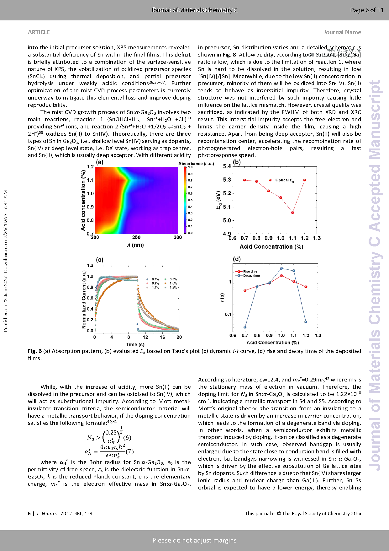
Fig. 6 (a) Absorption pattern, (b) evaluated E_g based on Tauc’s plot (c) dynamic I-t curve, (d) rise and decay time of the deposited films
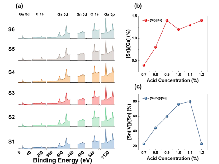
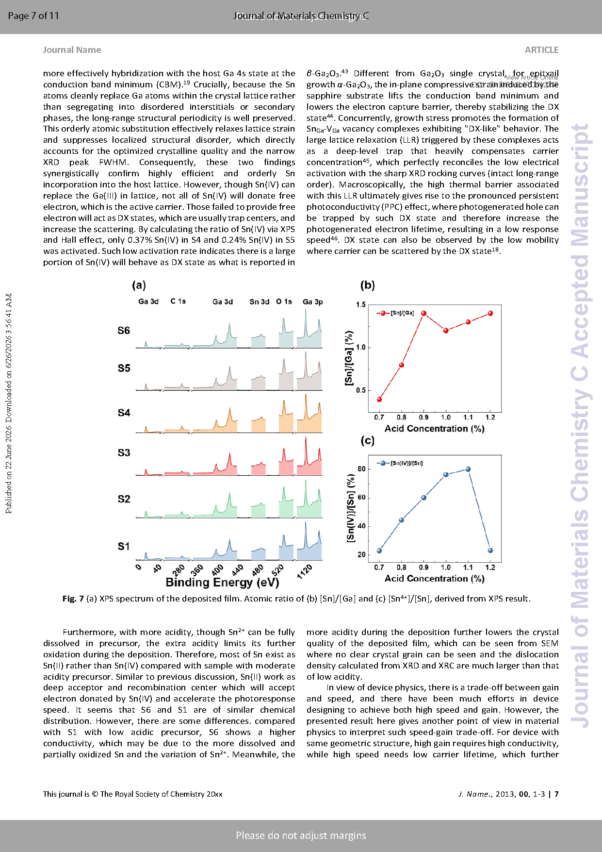
Fig. 7 (a) XPS spectrum of the deposited film. Atomic ratio of (b) [Sn]/[Ga] and (c) [Sn⁴⁺]/[Sn], derived from XPS result
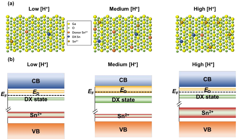
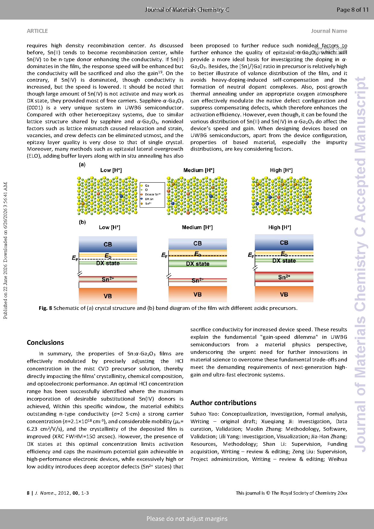
Fig. 8 Schematic of (a) crystal structure and (b) band diagram of the film with different acidic precursors
DOI :
10.1039/D6TC01273F
Instruction
Official Account

Cooperation
Top
