


Researchers from University of Illinois Chicago, University of Illinois Urbana-Champaign have published a dissertation titled " Effects of electrode geometry and sub-bandgap excitation in β-Ga₂O₃ photoconductive semiconductor switches " in Applied Physics Letters.
Background
Photoconductive semiconductor switches avoid signal backflow between high-voltage power modules and low-voltage control circuits, widely used in pulsed power, solid-state circuit breakers and electromagnetic launch systems. Ultra-wide bandgap β-Ga₂O₃ owns ultrahigh breakdown field, Fe-doped semi-insulating β-Ga₂O₃ is suitable for photoconductive switches. Conventional devices adopt above-bandgap UV excitation, photons are absorbed near material surface and carriers recombine seriously, limiting collection efficiency. Existing works only study single factor of excitation wavelength or electrode pitch, without joint optimization strategy. No unified figure of merit is proposed to evaluate device comprehensive performance, which restricts the design of high-power photoconductive switches.
Abstract
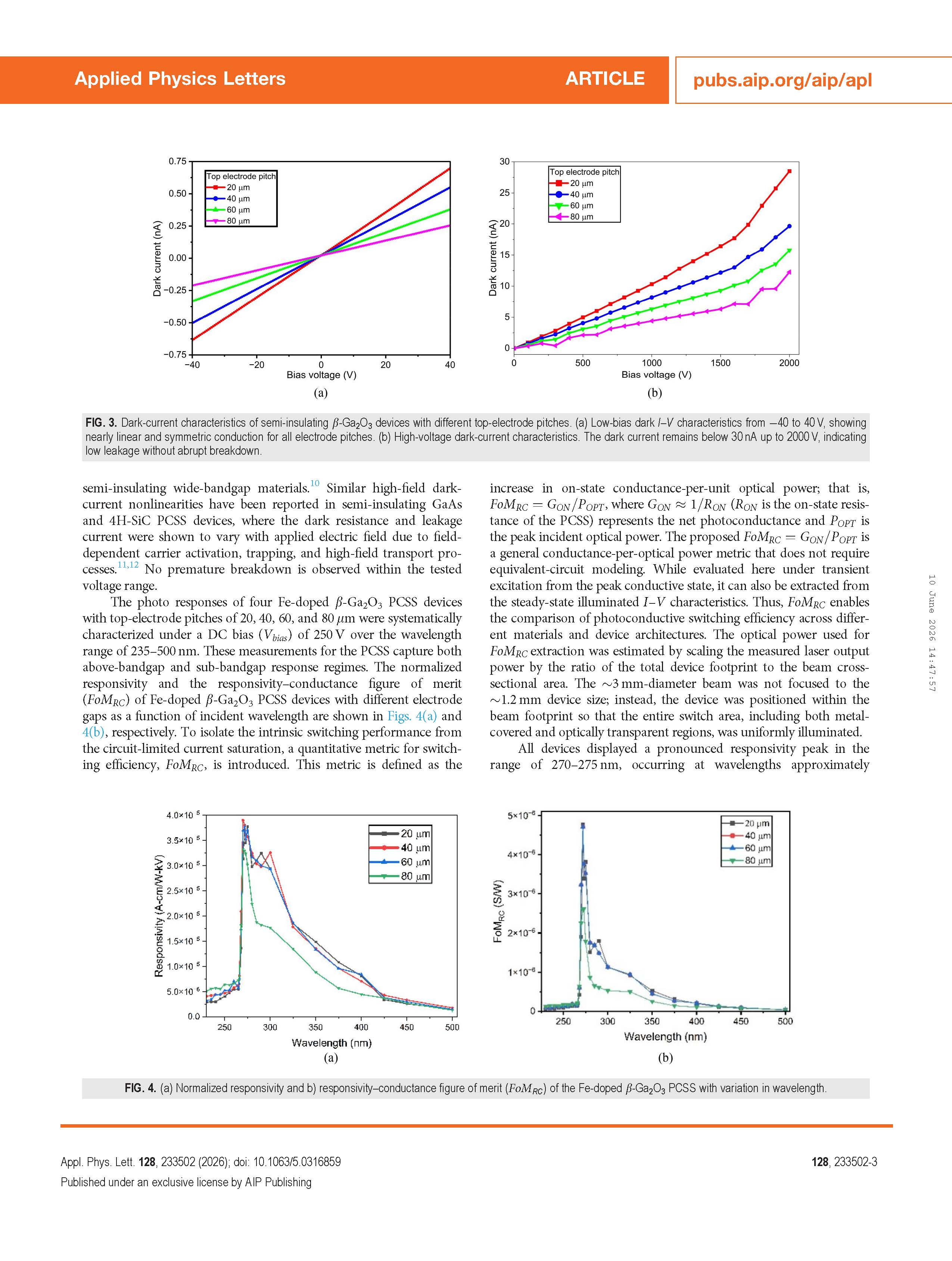
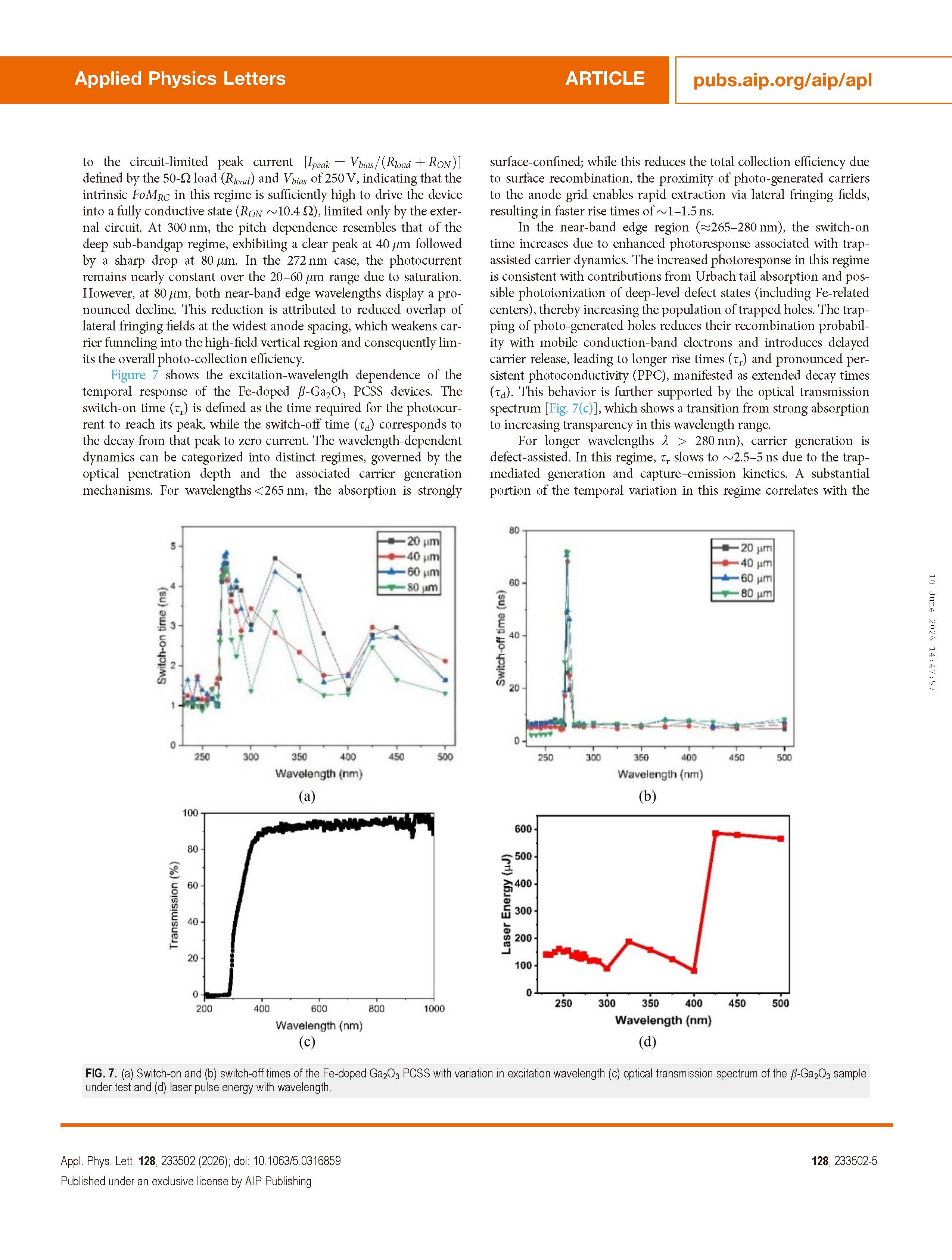
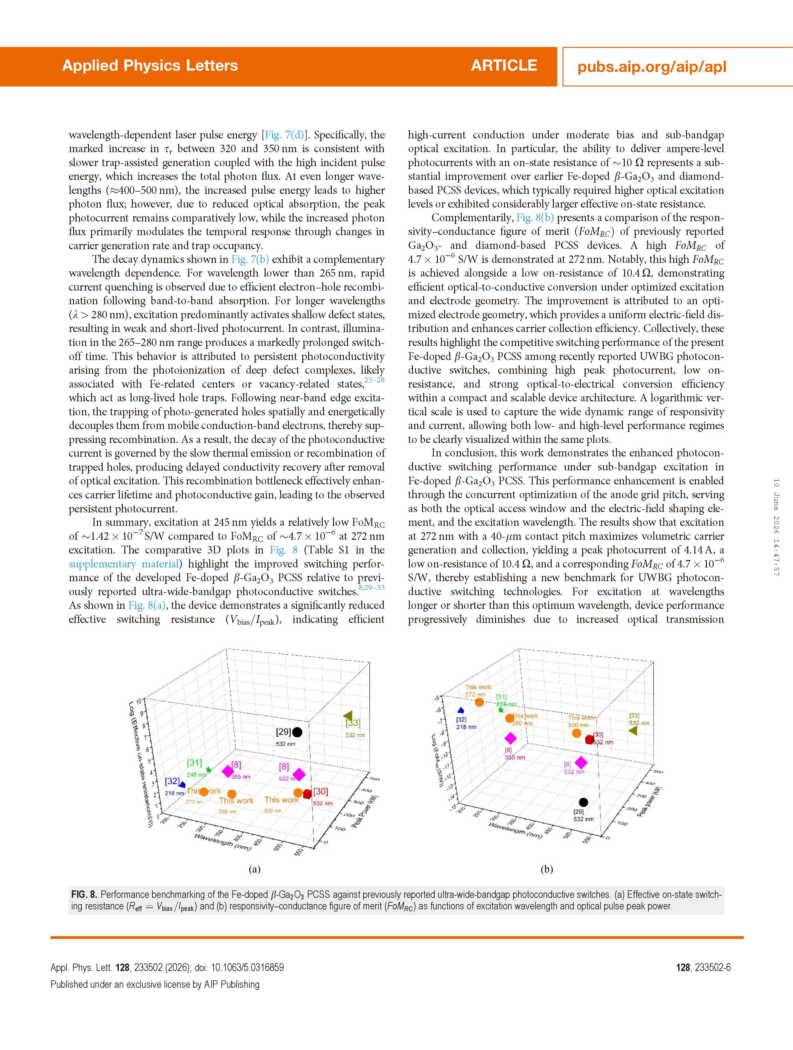
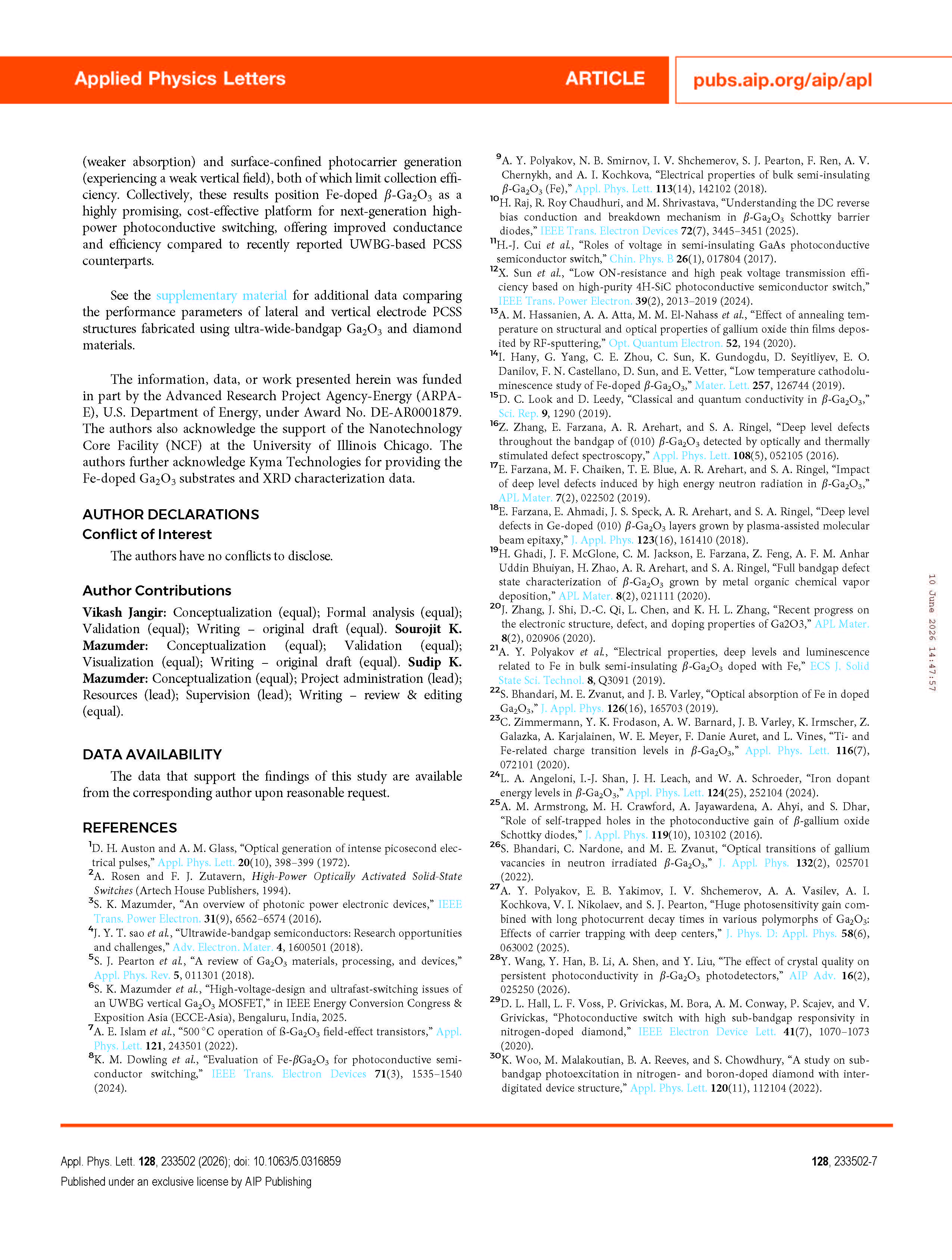
This work reports enhanced photoconductive switching performance in Fe-doped β-Ga₂O₃ PCSS by concurrently optimizing electrode geometry and the optical excitation wavelength. By systematically varying the anode grid pitch (20–80 μm) and excitation spectrum (235–500 nm), we identify a key sub-bandgap regime centered at 272 nm that activates deep-level defect states and enables efficient bulk carrier transport. In contrast to above-bandgap excitation, which is limited by shallow surface absorption, sub-bandgap illumination promotes strong photocurrent generation and improved carrier collection. Under optimized conditions with a 40 μm pitch, the device exhibits a high peak photocurrent of 4.14 A and a low on-resistance of 10.4 Ω. To quantify this simultaneous achievement, we define a responsivity–conductance figure of merit (FoMRC), which reaches a value of 4.7 ×10⁻⁶ S/W. These results underscore the strong potential of Fe-doped β-Ga₂O₃ for next-generation high-power optoelectronic switching, enabling robust ampere-level photocurrents together with low on-resistance through optimized device geometry and sub-bandgap excitation.
Highlights
Jointly optimize anode grid pitch and sub-band excitation wavelength for Fe-doped β-Ga₂O₃photoconductive switches.
Discover 272 nm sub-bandgap excitation window for efficient bulk carrier generation via Fe deep defects.
Propose a new responsivity–conductance figure of merit (FoMRC) for unified device performance evaluation.
Realize 4.14 A peak photocurrent and ultra-low on-resistance of 10.4 Ω under 40 μm electrode pitch.
Conclusion
In conclusion, this work demonstrates the enhanced photoconductive switching performance under sub-bandgap excitation in Fe-doped β-Ga₂O₃ PCSS. This performance enhancement is enabled through the concurrent optimization of the anode grid pitch, serving as both the optical access window and the electric-field shaping element, and the excitation wavelength. The results show that excitation at 272 nm with a 40 μm contact pitch maximizes volumetric carrier generation and collection, yielding a peak photocurrent of 4.14 A, a low on-resistance of 10.4 Ω, and a corresponding FoMRC of 4.7 ×10⁻⁶ S/W, thereby establishing a new benchmark for UWBG photoconductive switching technologies. For excitation at wavelengths longer or shorter than this optimum wavelength, device performance progressively diminishes due to increased optical transmission and surface-confined photocarrier generation (both of which limit collection efficiency). Collectively, these results position Fe-doped β-Ga₂O₃ as a highly promising, cost-effective platform for next-generation high-power photoconductive switching, offering improved conductance and efficiency compared to recently reported UWBG-based PCSS counterparts.
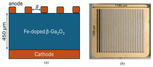
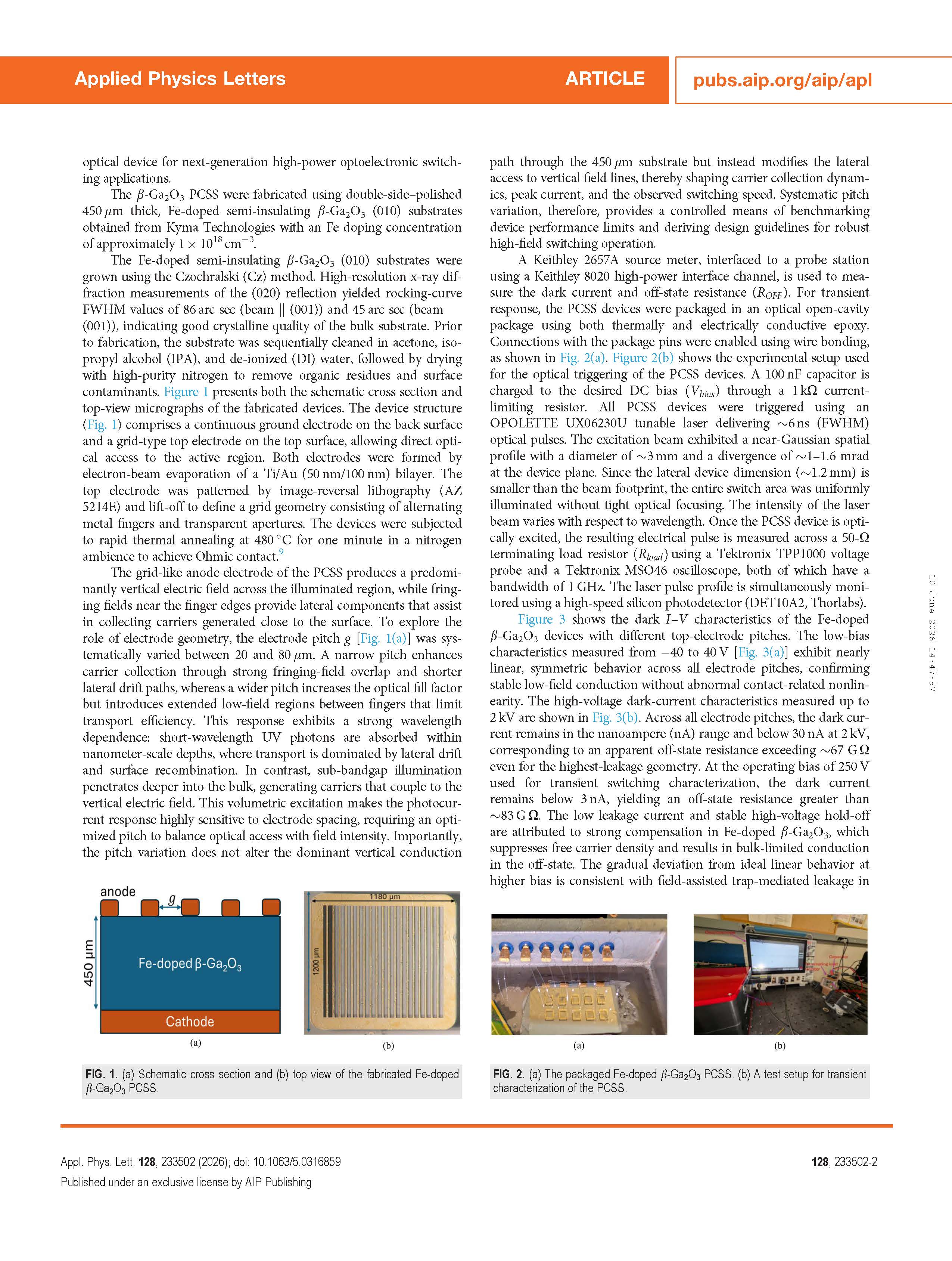
FIG. 1. (a) Schematic cross section and (b) top view of the fabricated Fe-doped β-Ga₂O₃ PCSS.
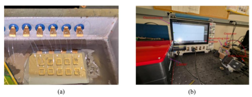
FIG. 2. (a) The packaged Fe-doped β-Ga₂O₃ PCSS. (b) A test setup for transient characterization of the PCSS.
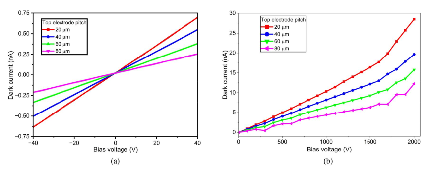
FIG. 3. Dark-current characteristics of semi-insulating b-Ga₂O₃ devices with different top-electrode pitches. (a) Low-bias dark I–V characteristics from −40 to 40 V, showing nearly linear and symmetric conduction for all electrode pitches. (b) High-voltage dark-current characteristics. The dark current remains below 30 nA up to 2000 V, indicating low leakage without abrupt breakdown.
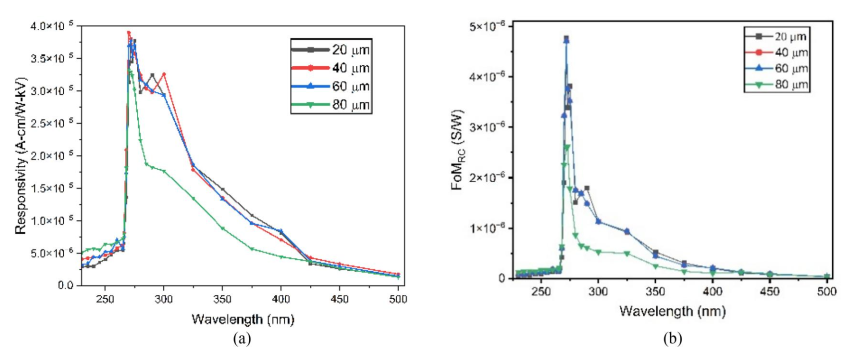
FIG. 4. (a) Normalized responsivity and (b) responsivity–conductance figure of merit (FoMRC) of the Fe-doped β-Ga₂O₃ PCSS with variation in wavelength.
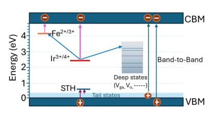
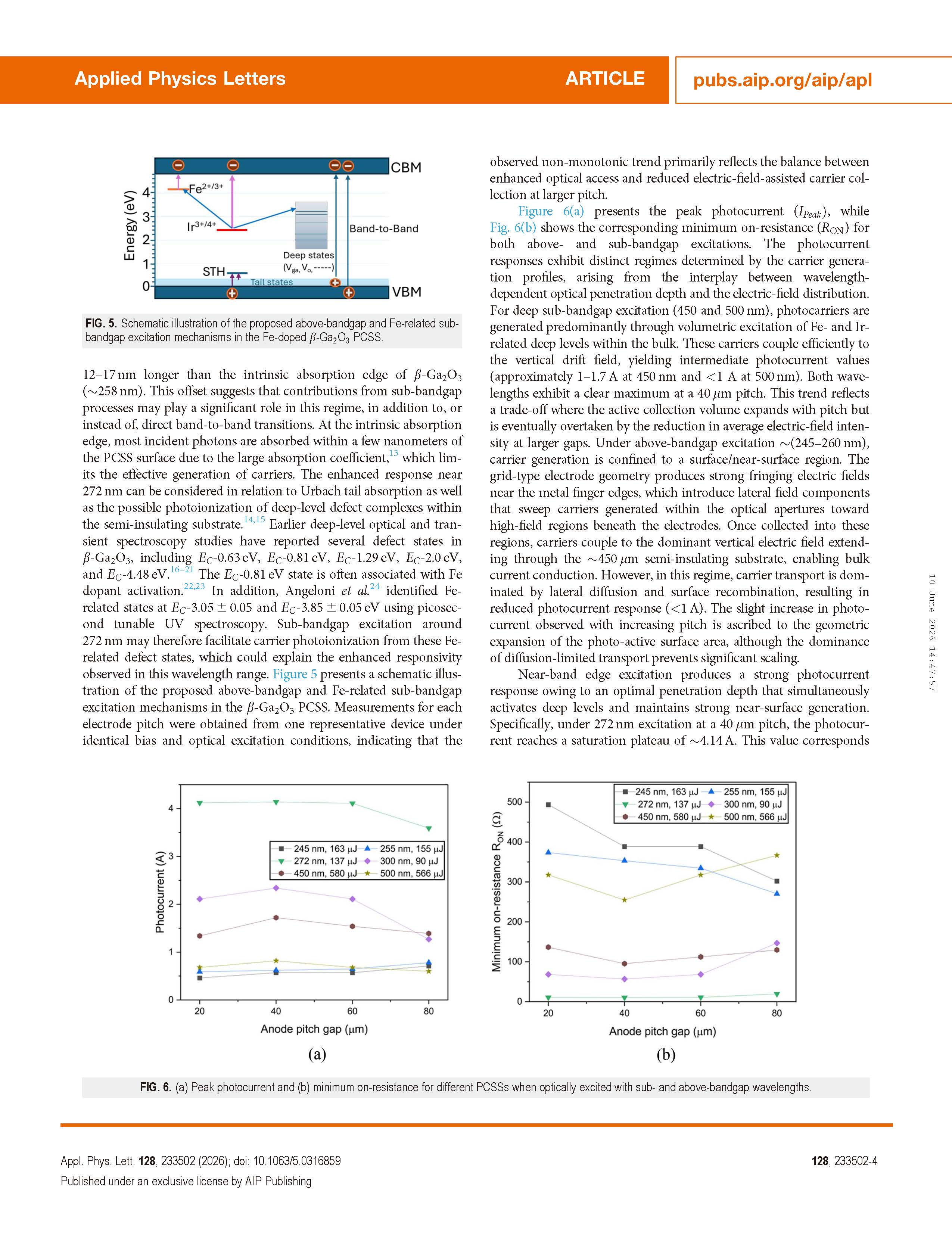
FIG. 5. Schematic illustration of the proposed above-bandgap and Fe-related sub-bandgap excitation mechanisms in the Fe-doped β-Ga₂O₃ PCSS.
DOI:
doi.org/10.1063/5.0316859

Instruction
Official Account

Cooperation
Top
