


Details of the Research
① Background and Technical Challenges
As a semiconductor material developed in Japan, β-Ga₂O₃ offers the advantages of low-cost crystal growth and extremely high breakdown voltage capability. Therefore, it is considered a promising next-generation power semiconductor material supporting the widespread adoption of electric vehicles, energy-efficient railway systems, and effective utilization of renewable energy sources such as solar and wind power.
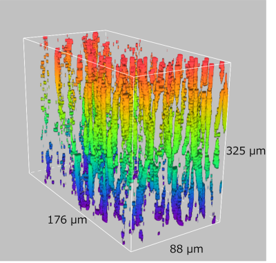
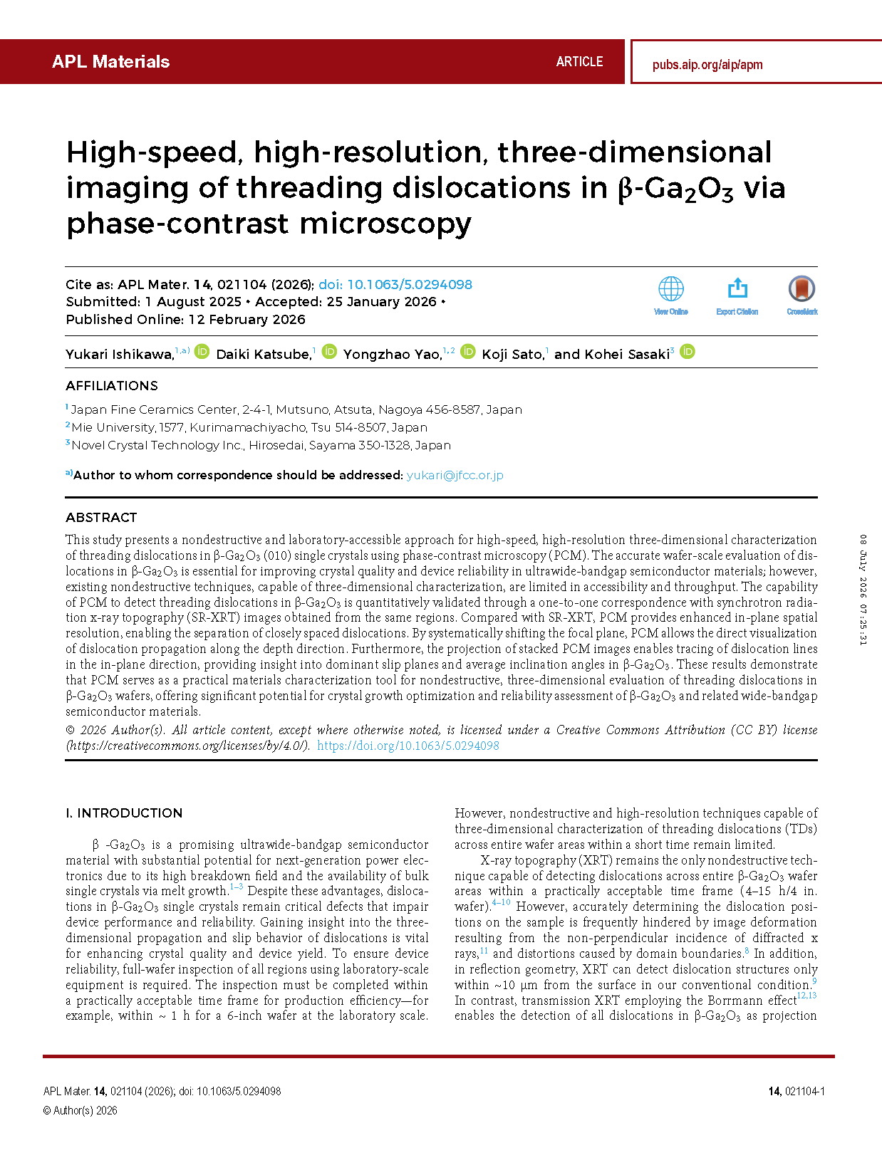
Figure 1. Three-dimensional reconstructed image of defects (dislocations) in a β-Ga₂O₃ (010) single crystal
Power devices are core technologies for efficiently converting and controlling electrical energy, playing an essential role in improving energy utilization efficiency and achieving a decarbonized society.
Among various wide-bandgap semiconductor materials, β-Ga₂O₃ not only exhibits excellent high-voltage operating capability but also features relatively easy crystal growth and suitability for fabricating large-size wafers.
However, crystal defects such as dislocations remain present inside β-Ga₂O₃ crystals. These defects not only degrade device performance but also affect long-term operational reliability.
Therefore, solving these challenges requires accurate understanding of the location, quantity, and distribution of defects inside crystals, and feeding this information back into the optimization of crystal growth processes.
To meet this requirement, there is an urgent need to establish an evaluation technology capable of high-speed and non-destructive defect detection across entire wafers.
Currently, one of the non-destructive techniques used to evaluate defect distributions in β-Ga₂O₃ is X-ray topography (Note 6).
By employing specially designed goniometers (Note 7), this method enables three-dimensional observation of defects inside crystals.
However, measurements and analyses using this technique require specialized knowledge of crystallography and X-ray diffraction, making it difficult for general researchers and engineers to use conveniently.
② Research Contents
In this study, β-Ga₂O₃ crystals were observed using phase-contrast microscopy, and the feasibility of high-speed defect evaluation over a large area was demonstrated.
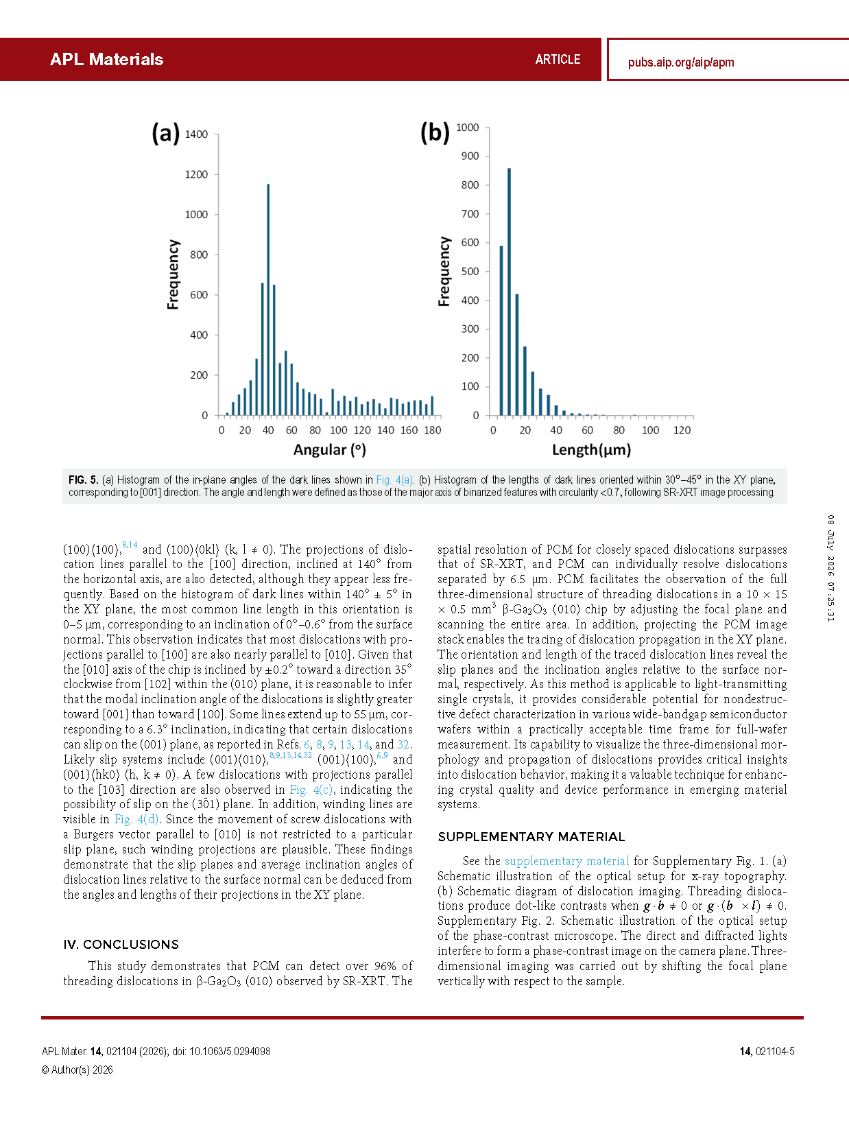
Each image covered an area of 360 μm × 300 μm and could be acquired within only 0.003 seconds. Based on calculations, approximately 170,000 images required for complete inspection of a 6-inch wafer (Note 8) could be captured in approximately 500 seconds.
Point-like contrast features were observed in the acquired images. Through comparison with other evaluation techniques, these features were confirmed to correspond to dislocations within the crystal.
Furthermore, the consistency rate with the results obtained by other evaluation methods exceeded 96%, demonstrating the high detection accuracy of this technique.
In addition, three-dimensional observations of the crystal interior were performed by continuously shifting the focal position from the upper surface to the lower surface of the crystal.
The results revealed that most dislocations penetrated through the crystal in an almost straight manner while being slightly inclined along a specific direction.
Meanwhile, various types of dislocation morphologies were also identified, including:
dislocations with different inclination directions;
dislocations that penetrate through the entire crystal but exhibit local bending or meandering behavior.
These findings demonstrate the diversity of dislocation morphologies in β-Ga₂O₃ crystals.
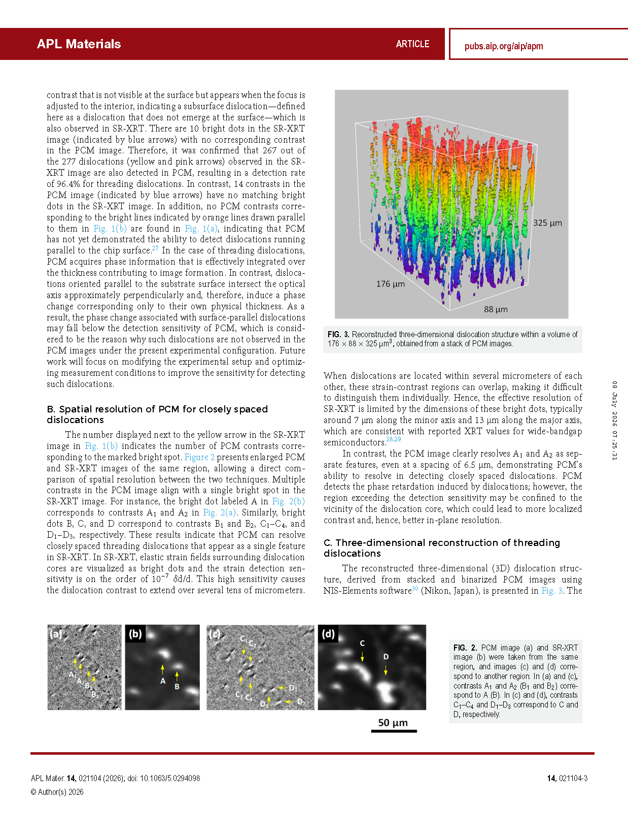
Furthermore, phase-contrast microscopy was able to individually distinguish closely spaced dislocations with a separation distance of approximately 6.5 μm, which could not be separated by X-ray topography.
These results indicate that this technology enables more accurate evaluation of dislocation distribution and density inside crystals.
③ Significance of the Results and Future Development
This study demonstrated that phase-contrast microscopy enables high-speed, large-area, three-dimensional observation of defects inside β-Ga₂O₃ crystals.
Compared with conventional methods, this technology enables non-destructive evaluation of entire wafers, which has previously been difficult to achieve, allowing comprehensive characterization of defect distribution and defect density throughout the crystal.
This capability represents a significant advancement in crystal quality evaluation.
In addition, the method features relatively simple operation and does not require highly specialized expertise.
Therefore, the technology is expected to be applied not only in research fields but also as a practical wafer inspection tool.
Because of its capability for high-speed and wide-area inspection, the technology has potential applications in in-line inspection and quality control processes within semiconductor manufacturing environments.
Furthermore, this technology can provide rapid and accurate feedback for optimizing crystal growth conditions, accelerating improvements in β-Ga₂O₃ crystal quality.
These advances are expected to enhance power device performance and long-term reliability, while promoting the wider adoption of β-Ga₂O₃ devices in fields including automobiles, railways, and power conversion systems.
In the future, the research team will continue to improve the accuracy and automation of this method, while enhancing defect classification capabilities and quantitative evaluation techniques.
The team also aims to expand the application of this technology to other wide-bandgap semiconductor materials, contributing to the development of next-generation power semiconductor materials.
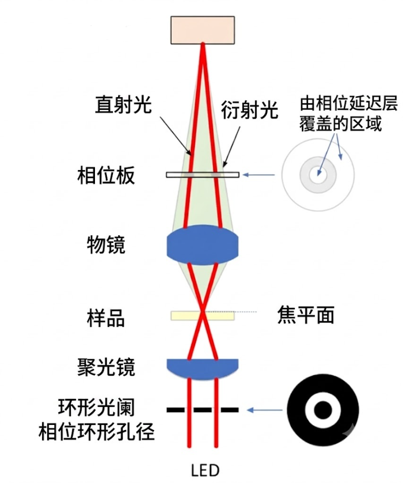
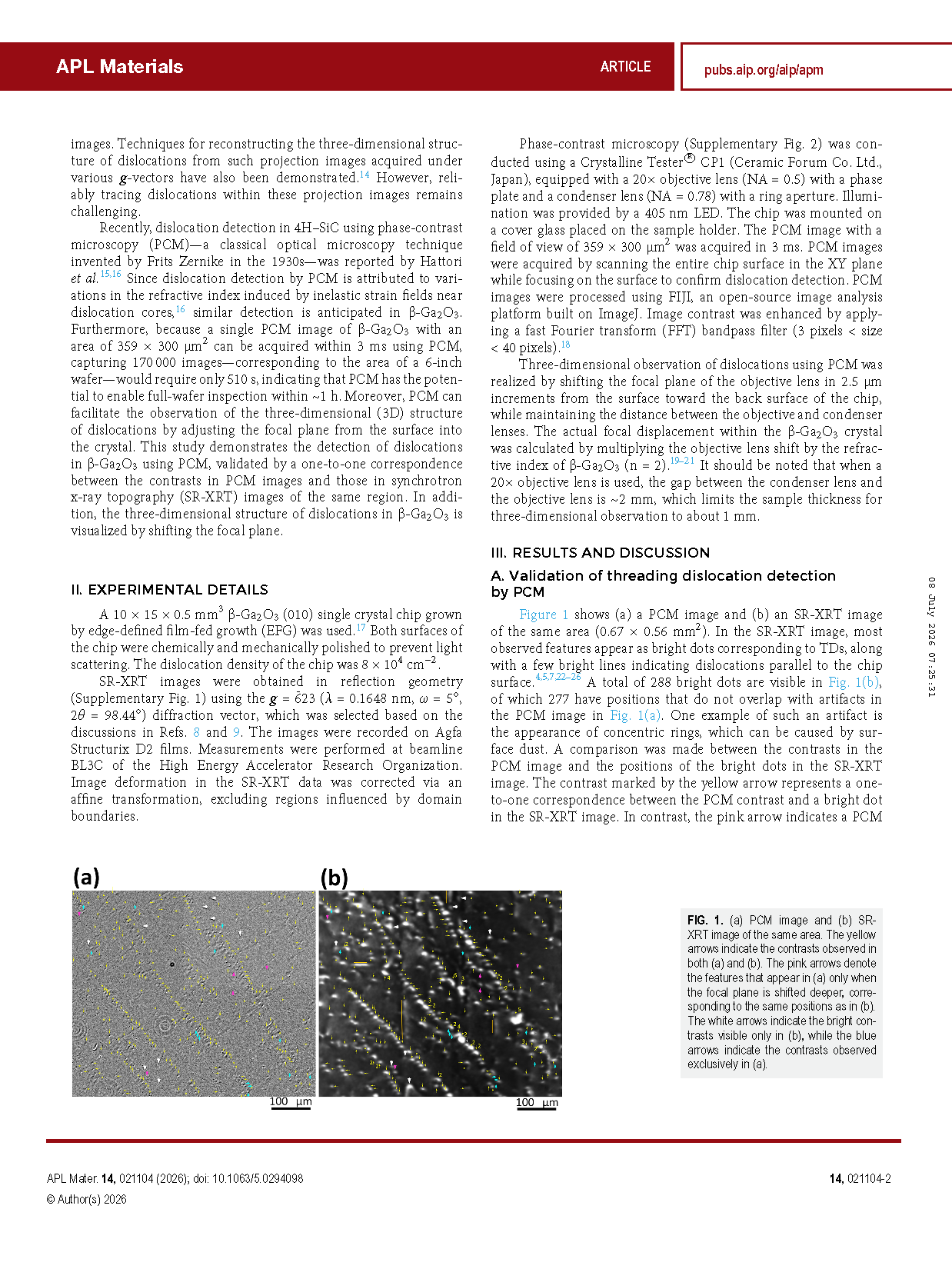
Figure 2. Schematic illustration of the optical system of phase-contrast microscopy
A phase image is generated through interference between direct light and diffracted light.
Three-dimensional observation is performed by moving the focal plane from the crystal surface into the interior along the direction perpendicular to the sample surface.
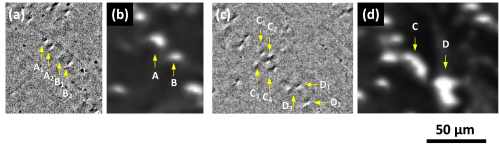
Figure 3. (a), (c) Phase-contrast microscopy images; (b), (d) X-ray topography images
Dislocation images A–D observed by X-ray topography can be further separated and identified as corresponding dislocation images Ai~Di using phase-contrast microscopy.
Publication Information
Title:
High-speed, high-resolution, three-dimensional imaging of threading dislocations in β-Ga₂O₃ via phase-contrast microscopy
Authors:
Yukari Ishikawa, Daiki Katsube, Yongzhao Yao, Koji Sato, Kohei Sasaki
Journal:
APL Materials
DOI:
10.1063/5.0294098
Instruction
Official Account

Cooperation
Top
