


Introduction:
In the Ga₂O₃ industrial chain, substrates serve as the starting point for epitaxial growth, device fabrication, and performance evaluation, making them a fundamental element that determines the pace of commercialization. As β-Ga₂O₃ single-crystal growth technology continues to advance, the global substrate market is evolving from small research-grade samples toward engineering-ready products featuring multiple crystal orientations, larger wafer sizes, customizable specifications, and compatibility with epitaxial growth.
Currently, commercially available Ga₂O₃ substrates are primarily differentiated by crystal phase, crystal orientation, wafer size, doping type, and epitaxial support capabilities. β-Ga₂O₃ single-crystal substrates remain the dominant product, with orientations such as (100), (010), (001), (011), and (−201) increasingly adopted for materials research and device development. At the same time, some suppliers have begun offering HVPE-, MOCVD-, and MBE-grown epitaxial wafers, driving the evolution of the Ga₂O₃ supply chain toward an integrated substrate–epitaxy–device validation ecosystem.
In this article, we review commercially available and customizable Ga₂O₃ substrate products, examining the current product landscape and commercialization progress from the perspectives of crystal orientation, wafer specifications, doping characteristics, and epitaxial support capabilities.
(001)Substrates:
For monoclinic β-Ga₂O₃, which exhibits strong crystallographic anisotropy, substrate orientation influences not only wafer processing and surface morphology, but also epitaxial growth behavior, defect evolution, and device architecture. Among commercially available Ga₂O₃ substrates, the (001) orientation has become one of the most widely adopted, serving as a primary platform for large-diameter substrate production and power device development.
From the global supply perspective, Novel Crystal Technology, Inc. (NCT, Japan) is one of the leading suppliers of (001)-oriented β-Ga₂O₃ substrates. NCT primarily employs the Edge-defined Film-fed Growth (EFG) method for β-Ga₂O₃ crystal growth. According to its publicly available product portfolio, the company offers 2-inch to 6-inch (001) substrates, with options including Sn-doped and unintentionally doped (UID) wafers to meet different application requirements.
In addition to substrates, the (001) orientation has become the principal platform for commercial β-Ga₂O₃ epitaxial wafers. NCT supplies 2-inch and 4-inch β-Ga₂O₃ (001) HVPE epitaxial wafers, with customizable epitaxial layer thicknesses and doping concentrations within specified ranges.
For high-voltage power devices, the drift layer thickness, carrier concentration, and defect density of the epitaxial layer directly determine key performance metrics such as breakdown voltage (BV), specific on-resistance (Rₒₙ,ₛₚ), and reverse leakage current. Therefore, the integrated supply of (001) substrates together with HVPE epitaxial wafers represents an important step in advancing Ga₂O₃ from material research toward power device validation and commercialization.
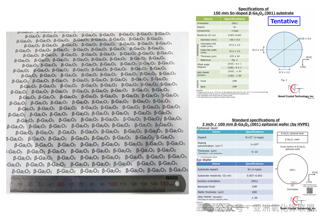
Figure 1. NCT β-Ga₂O₃ (001) substrate and epitaxial wafer products [1]
Kyma Technologies (USA) is also advancing epitaxial growth services based on (001) β-Ga₂O₃ substrates. According to its publicly available information, Kyma provides Ga₂O₃ epitaxy services on both (001) and (010) β-Ga₂O₃ substrates, and can fabricate lightly doped thick epitaxial layers on (001) substrates with thicknesses exceeding 10 μm and free carrier concentrations below 10¹⁶ cm⁻³ [2]. Such thick epitaxial layers represent a critical material foundation for kV-class power devices.
In China, (001) substrates are also an important direction for large-scale production and engineering development. Garen Semiconductor (Hangzhou) is primarily pursuing the β-Ga₂O₃ single-crystal substrate route based on the edge-defined film-fed growth (EFG) method. Currently, the company has advanced the development and production of 2–6 inch EFG β-Ga₂O₃ single-crystal substrates, while continuing efforts in crystal size expansion, orientation control, defect suppression, process consistency, and epitaxial compatibility optimization.
Recently, Shandong SINOGa Vally Technology Co., Ltd. publicly reported the successful development of a 6-inch β-Ga₂O₃ single crystal with a (001) main surface and zero twin defects [3]. In addition, domestic companies including Hangzhou Garen Semiconductor and Fujia Gallium Industry have also established layouts in (001)-oriented β-Ga₂O₃ substrates and related products, further enriching China’s supply ecosystem for (001) β-Ga₂O₃ materials.
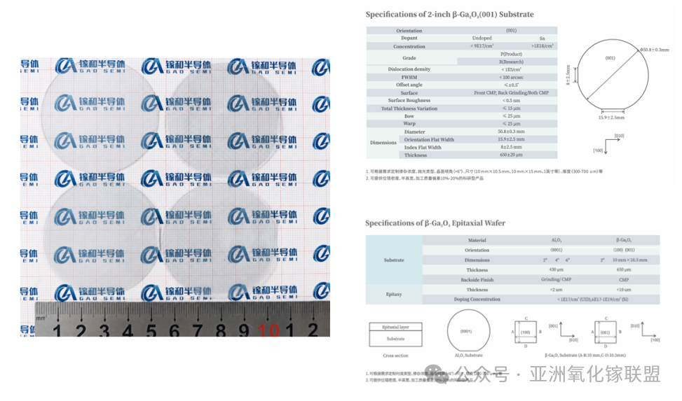
Fig. 2. (001) β-Ga₂O₃ substrate and epitaxial wafer products from GAO Semiconductor
(100)Substrates:
In addition to the (001) orientation, (100) β-Ga₂O₃ substrates have also attracted increasing attention in recent years. For monoclinic β-Ga₂O₃ crystals with strong anisotropy, different crystallographic orientations can lead to variations in surface structure, step evolution, epitaxial growth behavior, and electric field distribution within devices. (100) substrates are not only used for fundamental studies of epitaxial mechanisms but are also gradually becoming an important material platform for high-voltage MOSFETs, heterojunction diodes, and wafer-level device demonstrations.
At the international level, Novel Crystal Technology, Inc. (NCT, Japan) has included (100)-oriented β-Ga₂O₃ single-crystal substrates in its publicly available product portfolio, although they are currently mainly supplied in small-size formats. Compared with its (001) substrates available in 2–6 inch sizes, NCT’s (100) substrates are currently more focused on research applications. From the perspective of device development, (100) β-Ga₂O₃ substrates have demonstrated considerable application potential. Recent studies have reported 2-inch Si-doped β-Ga₂O₃ (100) homoepitaxial wafers and high-voltage MOSFET arrays [4]. The epitaxial layers were grown by MOCVD, achieving an average XRD rocking curve full width at half maximum (FWHM) of approximately 27.0 arcsec and a surface roughness below 1 nm. The fabricated devices exhibited breakdown voltages exceeding 3 kV, demonstrating the potential of (100) orientation for wafer-scale high-voltage device uniformity evaluation.
In China, several companies have also established layouts in (100)-oriented β-Ga₂O₃ substrates and epitaxial wafers. Companies including GAO Semiconductor, Fujia Gallium, and Garen Semiconductor have made progress in the development of (100)-oriented single-crystal substrates and epitaxial materials. Overall, China’s (100)-oriented β-Ga₂O₃ materials are gradually advancing toward larger-size substrates and device-grade epitaxial wafer applications.
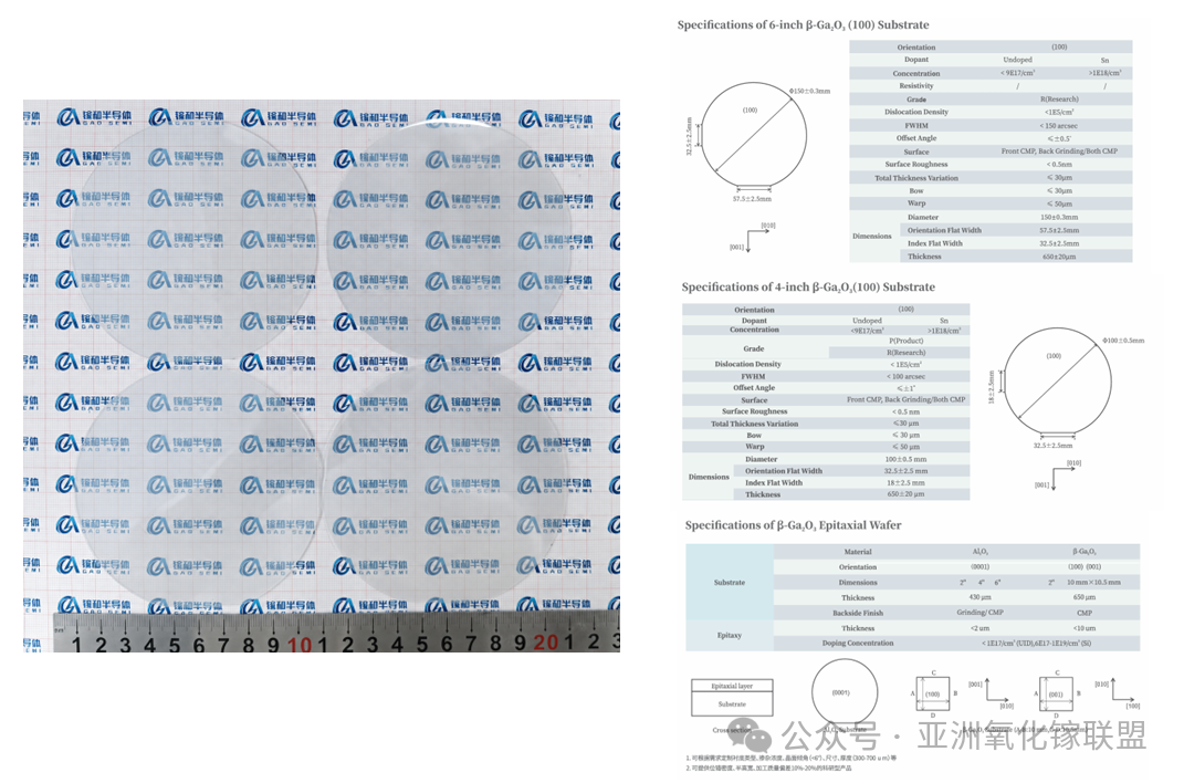
Fig. 3. GAO’s (100) β-Ga₂O₃ substrate and epitaxial wafer products
(010)Substrates:
The (010) orientation is one of the earliest studied and most extensively investigated β-Ga₂O₃ substrate types, playing an important role in epitaxial growth, surface engineering, channel material development, and device structure validation. Research has demonstrated that high-quality homoepitaxial β-Ga₂O₃ layers can be achieved on (010) substrates using techniques such as MOCVD and MBE. However, the surface morphology of epitaxial films is highly sensitive to substrate offcut angle, surface preparation conditions, and growth parameters. Therefore, the surface specifications and processing quality of (010) substrates are critical for subsequent epitaxial growth.
From the perspective of international supply, Novel Crystal Technology, Inc. (NCT, Japan) has included (010)-oriented β-Ga₂O₃ single-crystal substrates in its product portfolio. Similar to its (100) products, these substrates are currently mainly supplied in small-size formats of 10 × 15 mm². Compared with (001) substrates, which are more focused on large-size scaling and commercial development, (010) substrates are primarily used for epitaxial mechanism studies, surface morphology control, and fundamental device demonstrations, making them an important platform for crystallographic orientation engineering in β-Ga₂O₃ research.
In China, the scale-up of (010)-oriented β-Ga₂O₃ substrates is also progressing. Hangzhou Garen Semiconductor has successfully achieved the growth of 6-inch (010)-oriented β-Ga₂O₃ crystals using the vertical Bridgman (VB) method. In addition, domestic companies including GAO Semiconductor and Fujia Gallium are also advancing the development of multi-orientation β-Ga₂O₃ substrate products.
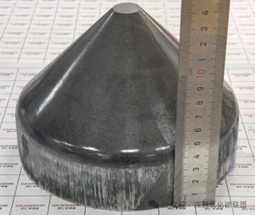
Fig. 4. (010)-oriented β-Ga₂O₃ crystal ingot grown by the VB method by Garen Semiconductor [5]
(-201)Substrates:
The (-201) orientation is one of the representative crystal planes among β-Ga₂O₃ substrate products. Compared with orientations such as (001) and (100), which have received greater attention for large-scale commercialization, (-201) substrates are more commonly used for vertical device demonstrations, surface barrier engineering, and comparative studies of epitaxial growth.
From the perspective of international supply, Novel Crystal Technology, Inc. (NCT, Japan) has included (-201)-oriented β-Ga₂O₃ single-crystal substrates in its publicly available product portfolio, with 2-inch substrates listed among its offerings. In China, (-201)-oriented substrates also represent an important part of β-Ga₂O₃ substrate development. Although they are not currently the largest-volume supplied orientation, (-201) substrates continue to play an important role in crystallographic orientation comparison, epitaxial mechanism studies, and device structure validation.
(011)Substrates:
The (011) orientation is an emerging crystal plane that has attracted increasing attention in β-Ga₂O₃ substrate development in recent years. It provides a new material option for crystallographic orientation engineering, homoepitaxial optimization, and high-voltage device evaluation.
From the international supply perspective, NCT has listed (011)-oriented β-Ga₂O₃ substrates and HVPE epitaxial wafers in its product portfolio. Among them, (011) HVPE epitaxial wafers are available in 10 × 15 mm² and 2-inch formats, targeting next-generation power device development. This indicates that (011) orientation has gradually progressed beyond fundamental crystallographic research and entered the stage of epitaxial wafer supply and device validation.
In China, notable progress has also been made in the development of (011)-oriented β-Ga₂O₃ substrates. According to publicly available information, Fujia Gallium has achieved stable batch supply capability for (011)-oriented β-Ga₂O₃ single-crystal substrates [6]. Meanwhile, GAO Semiconductor, Garen Semiconductor, and other domestic companies are continuing to expand their multi-orientation β-Ga₂O₃ substrate portfolios and provide certain small-size substrates with specialized crystal orientations, supporting research validation, epitaxial process development, and device structure exploration.
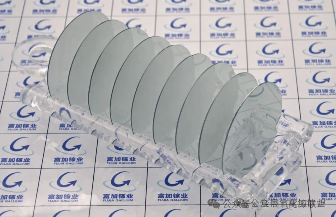
Fig. 5. (011)-oriented β-Ga₂O₃ substrate from Fujia Gallium [6]
Summary
Overall, β-Ga₂O₃ substrate products are gradually transitioning from early-stage small-size research samples toward a product-oriented stage featuring multiple crystallographic orientations, larger wafer sizes, diverse doping types, and integrated epitaxial support. Among these, the (001) orientation remains the dominant choice for large-size substrate supply and high-voltage power device demonstrations.
From the perspective of supplier development, Novel Crystal Technology, Inc. (NCT, Japan) remains one of the leading global suppliers of β-Ga₂O₃ substrates and epitaxial wafers, while Kyma Technologies focuses more on epitaxial services and device-grade material support. In China, companies including GAO Semiconductor, Garen Semiconductor, Fujia Gallium, and SINOGa Vally are continuously advancing β-Ga₂O₃ substrate technologies across different orientations, wafer sizes, and crystal growth approaches, contributing to a diversified development landscape involving multiple routes such as the edge-defined film-fed growth (EFG) method, casting method, and vertical Bridgman (VB) method.
Looking ahead, competition in the β-Ga₂O₃ substrate industry will no longer focus solely on achieving larger wafer sizes, but will increasingly shift toward achieving higher and more consistent material quality. Key factors including crystal quality, twin and defect control, within-wafer uniformity, processing yield, doping controllability, and epitaxial compatibility will collectively determine whether substrates can effectively support high-voltage power devices and large-scale commercialization.
With continued investment from both domestic and international companies, the β-Ga₂O₃ substrate supply chain is gradually moving beyond the material breakthrough stage and entering a critical phase of engineering validation and ecosystem development.
References:
[1]https://www.novelcrystal.co.jp/eng/2026/2926/
[2]https://www.kymatech.com/sub-divided-products/gallium-oxide
[3]https://mp.weixin.qq.com/s/tbv8GZWGm85z01Fb-jUnMw
[4]Liu N T, et al. arXiv:2606.07973 (2026)https://arxiv.org/abs/2606.07973
[5] https://mp.weixin.qq.com/s/iKgLgFSdgE0hZi3kEXc01w
[6]https://mp.weixin.qq.com/s/ODQZ0EIKtmoQ9q2jkxnG7A
Instruction
Official Account

Cooperation
Top
