


At present, high-quality gallium oxide substrates produced by Hangzhou Garen Semiconductor Co., Ltd. (hereinafter referred to as “Garen Semiconductor”) have been supplied in stable volumes to NextGO.Epi, a leading European technology company. This marks the transition of the cooperation between the two companies into a new stage of long-term and stable procurement.
The partnership originated from a global strategic agreement signed in May 2025. Since then, Garen Semiconductor’s products have undergone multiple rounds of performance verification and process compatibility evaluations. Ultimately, their outstanding performance has earned strong recognition from the customer.
NextGO.Epi is a leading European technology company specializing in gallium oxide epitaxy. The company has accumulated extensive expertise in epitaxial processes and device development, with multiple international patents and collaborations with several European universities. Its requirements for substrate suppliers are highly stringent—not only must the substrate itself meet strict quality standards, but suppliers must also demonstrate continuous, stable, and predictable delivery capabilities.
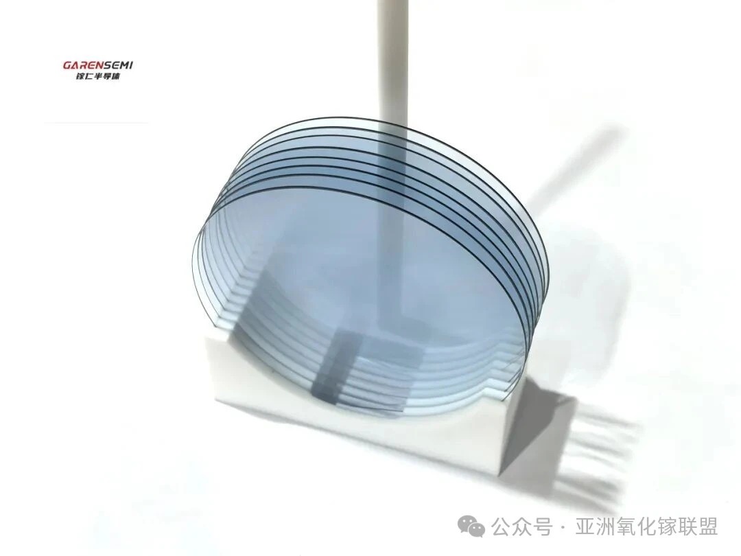
Figure 1. Garen Semiconductor gallium oxide substrates
Self-Developed Technology Enables High-Quality Substrate Production
Previously, the mainstream global technology route for gallium oxide substrates was represented by the Edge-defined Film-fed Growth (EFG) method developed by Japanese companies. Although this technology has achieved a high level of maturity, its key limitation lies in the reliance on expensive iridium crucibles, which directly restricts production expansion and cost reduction. This also creates uncertainties for downstream customers in terms of delivery schedules and pricing.
Based on its independently developed casting method, Garen Semiconductor has established a differentiated technology route featuring Chinese innovation. This approach significantly reduces the consumption of precious iridium materials and substantially lowers production costs. The crystal growth efficiency is more than 10 times higher than that of the EFG method, while enabling the growth of ultra-thick crystals with higher wafer yield per ingot. The process is also simpler and more controllable, removing key barriers toward large-scale production.
According to evaluations conducted by NextGO.Epi, substrates supplied by Garen Semiconductor demonstrate excellent crystal quality, with the X-ray rocking curve full width at half maximum (FWHM) below 90 arcsec, significantly outperforming comparable products.
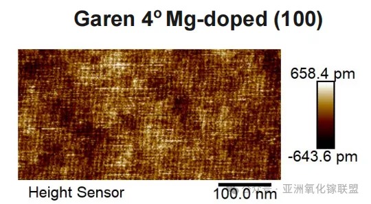
Figure 2. Testing results of Garen Semiconductor substrates
Validated by Leading Customers: Stable and Reliable Performance
Over the past year, Garen Semiconductor’s gallium oxide substrates have undergone multiple rounds of performance validation and process adaptation evaluations by NextGO.Epi.
Using Garen Semiconductor substrates, NextGO.Epi successfully achieved epitaxial layer growth with thicknesses reaching 450 nm. For the (100) crystal orientation, an electron mobility of 140 cm²/V·s was achieved at a carrier concentration of 4×10¹⁷ cm⁻³. For the (010) crystal orientation, an electron mobility of 135 cm²/V·s was achieved at a carrier concentration of 5×10¹⁷ cm⁻³.
The epitaxial wafers demonstrated stable and reliable performance, with overall properties exceeding those of comparable products. Gallium oxide power devices fabricated on these epitaxial wafers are expected to achieve higher breakdown capability and lower conduction losses.
This performance is enabled by Garen Semiconductor’s unique fully self-controlled “equipment–crystal growth–substrate–epitaxy” integrated technology system, which ensures excellent batch-to-batch consistency and further strengthens the strategic cooperation between the two companies.
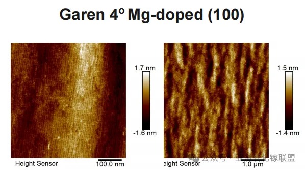
Figure 3. Testing results of NextGO.Epi epitaxial wafers (based on Garen Semiconductor substrates)
Amid global technological competition and collaboration, gallium oxide has increasingly become a strategic material attracting worldwide attention. During China’s 15th Five-Year Plan period, the industrialization of ultra-wide-bandgap semiconductor materials such as gallium oxide and diamond is expected to receive further support. Gallium oxide is rapidly emerging as one of the most promising materials for next-generation power semiconductor markets.
Looking ahead, Garen Semiconductor will continue deepening cooperation with high-quality global partners such as NextGO.Epi. Leveraging its technological advantages in the casting method and its fully integrated, independently controlled industrial capabilities, the company aims to jointly overcome key challenges in the commercialization of ultra-wide-bandgap semiconductors and contribute Chinese innovation to the global semiconductor industry.
About Garen Semiconductor
Hangzhou Garen Semiconductor Co., Ltd. is a global provider of gallium oxide materials and equipment solutions, specializing in the R&D and commercialization of ultra-wide-bandgap semiconductor technologies. The company’s core products include 2–8 inch gallium oxide single crystals and substrates (including the world’s first 8-inch products), vertical Bridgman (VB) gallium oxide crystal growth equipment, and 2–8 inch gallium oxide homoepitaxial wafers (including the world’s first 8-inch products). Garen Semiconductor is dedicated to building a fully integrated “equipment–crystal growth–substrate–epitaxy” industrial ecosystem and providing comprehensive solutions for global customers. The company’s achievements in gallium oxide have been widely recognized and featured by leading media outlets, including People’s Daily, Xinhua News Agency, Science and Technology Daily, Sina Finance, China Blue News, and The Paper.
For more information, please visit the official website: http://garen.cc/
Or contact us:
Mr. Jiang
Phone: +86 159 1871 9807
Email: jiangjiwei@garen.cc
Mr. Xia
Phone: +86 190 1127 8792
Email: xianing@garen.cc
Instruction
Official Account

Cooperation
Top
