


Major News
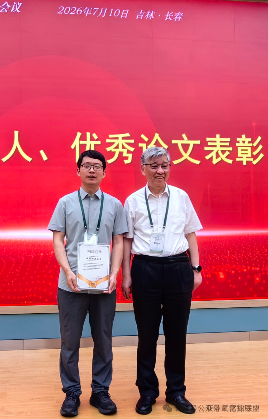
Recently, at the 2025 Editorial Board Meeting of the Journal of Synthetic Crystals, the paper “Growth and Characterization of Ga₂O₃ Single Crystals by the Vertical Bridgman Method”, jointly published by Fujia Gallium and the Shanghai Institute of Optics and Fine Mechanics in February 2025, was honored as one of the Top 10 Outstanding Papers of the Year. The award was presented in recognition of the paper's outstanding annual download and citation performance, as well as its strong peer recognition. This honor also reflects the high level of attention from the research community to the team's significant progress in β-Ga₂O₃ single-crystal materials.
Award-Winning Paper Highlights Innovation in the VB Growth Method
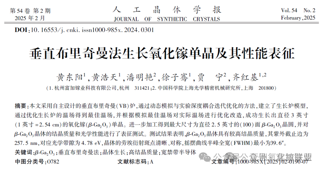
In July 2024, the team successfully grew a large-size β-Ga₂O₃ single crystal for the first time in China using a self-developed vertical Bridgman (VB) crystal growth furnace. This achievement was made possible through an iterative approach that tightly integrated dynamic simulation with experimental optimization.
Characterization results demonstrated excellent crystal quality, including a UV cutoff wavelength of 257.5 nm, corresponding to an optical bandgap of 4.78 eV. The crystal also exhibited clear and symmetric Laue diffraction patterns, while the minimum full width at half maximum (FWHM) of the X-ray rocking curve reached 39.6 arcsec.
Since its publication in February 2025, the paper has attracted significant attention from the research community, accumulating more than 3,000 downloads and ranking among the leading papers of the same period in terms of total citations.
Advantages of the Vertical Bridgman (VB) Method for Ga₂O₃ Single-Crystal Commercialization
Gallium oxide (Ga₂O₃), an ultra-wide-bandgap semiconductor, has broad application prospects in high-voltage power electronics and solar-blind ultraviolet photodetection. However, the ability to grow large-size, high-quality, and low-cost single crystals remains the primary bottleneck to its commercialization. Among the available crystal growth technologies, the Vertical Bridgman (VB) method is regarded as one of the most promising routes for large-scale Ga₂O₃ production due to its relatively low equipment investment, stable growth process, and strong scalability for mass manufacturing. Fujia Gallium became one of the first companies in China to strategically invest in VB-grown Ga₂O₃ single crystals in 2023. Guided by its dual-engine strategy of equipment innovation and process optimization, the company achieved major technological breakthroughs within a short period by leveraging high-precision thermal field simulation. Notably, Novel Crystal Technology (NCT) of Japan, a leading Ga₂O₃ company, has also identified the VB method as a core technology for future large-diameter Ga₂O₃ crystal production after years of development, further highlighting the significant potential of the VB method for the industrial-scale manufacturing of Ga₂O₃ single crystals.
From Research to Mass Production: Rapid Breakthroughs in Technology and Equipment
Following the publication of this paper, Fujia Gallium has accelerated its commercialization efforts. In September 2025, the company achieved the first domestic demonstration of 6-inch β-Ga₂O₃ single-crystal growth using the VB method. In December of the same year, it successfully produced the world’s first 8-inch VB-grown Ga₂O₃ crystal. In March 2026, Fujia Gallium further achieved another milestone by growing the world’s first 12-inch VB-grown Ga₂O₃ crystal. Behind each increase in crystal size lies a substantial improvement in growth processes and equipment capabilities, representing a solid step toward large-scale industrialization.
Through continuous optimization of growth technologies, Fujia Gallium has established independent intellectual property barriers covering both process technologies and equipment systems. In the field of VB crystal growth processes, the company has filed six invention patents, while in VB growth equipment development, it has obtained four internationally granted patents. In addition, in 2025, Fujia Gallium led the drafting of China’s first national standard in the field of gallium oxide single crystals, “Gallium Oxide Single-Crystal Polished Wafers” (Project No. 20254547-T-469), further contributing to the standardization and industrial development of the Ga₂O₃ semiconductor industry.
Targeting Downstream Applications: Building a Trusted Ga₂O₃ Substrate Supplier
As the first domestic Ga₂O₃ materials supplier to strategically adopt the VB technology route, Fujia Gallium has established a clear market positioning: addressing the practical needs of downstream customers in power electronics and optoelectronic detection, while providing high-quality Ga₂O₃ substrates and related products. Currently, the company has developed a comprehensive product portfolio covering 2-inch to 8-inch Ga₂O₃ substrates and epitaxial wafers, including EFG/VB-grown substrates, MOCVD/MBE epitaxial wafers, and fully automated crystal growth equipment. Its products and solutions have been delivered to more than 60 universities, research institutes, and industrial customers worldwide.
Recognition represents affirmation of past achievements, while products represent commitments to future development. Moving forward, Fujia Gallium will continue to pursue technological innovation and remain customer-focused, upholding its mission of “Enabling the world with better materials” to provide a solid material foundation for the development of fourth-generation semiconductor technologies.
Product Portfolio
Gallium Oxide Crystal Growth Equipment
Fujia Gallium has developed the world’s first EFG crystal growth system featuring a proprietary “one-click crystal growth” function, supporting 2-inch to 8-inch crystal production. The system is protected by 6 granted domestic patents and 4 international patents. Complete equipment solutions and process packages are available. The company has also independently developed fully automated VB (Vertical Bridgman) crystal growth equipment and was the first in China to overcome the technical bottleneck of 12-inch Ga₂O₃ single-crystal growth using the VB method, enabling the production of large-diameter bulk crystals. Currently, this equipment has been granted 6 domestic patents and 4 international patents, and VB systems along with process packages can be provided based on customer requirements.
Gallium Oxide Single-Crystal Substrates
As one of China’s earliest pioneers in Gallium Oxide single-crystal research and an industry-leading supplier, Fujia Gallium provides high-quality single-crystal substrates to global customers. The product portfolio includes 26 standard Ga₂O₃ substrate specifications covering diameters from 2 to 8 inches. Customized solutions are available in terms of wafer size, electrical properties, and crystal orientation, supporting both advanced epitaxy R&D and volume production requirements.
Gallium Oxide Epitaxial Wafers
Built upon mature MOCVD (Metal-Organic Chemical Vapor Deposition) and MBE (Molecular Beam Epitaxy) platforms, Fujia Gallium offers 15 standard epitaxial wafer products from 2-inch to 6-inch formats, as well as customized MBE-based epitaxial structures. The company provides integrated “substrate + epitaxy” solutions. A precise process control system enables customization of key parameters including epitaxial layer thickness, doping concentration, and compositional uniformity, meeting diverse requirements across different power levels and device architectures.
About Hangzhou Fujia Gallium
Hangzhou Fujia Gallium Technology Co., Ltd., established on December 31, 2019, is committed to its vision of “Bringing Better Materials to the World” and focuses on the industrialization of ultra-wide bandgap gallium oxide semiconductor materials. Its core products include gallium oxide single-crystal substrates, MOCVD/MBE epitaxial wafers, and crystal growth equipment based on the Vertical Bridgman (VB) and Edge-Defined Film-Fed Growth (EFG) methods. The company provides systematic solutions for material development, accelerating the integration of the entire ultra-wide bandgap gallium oxide industry chain and promoting the application of gallium oxide materials in power devices, microwave RF devices, and optoelectronic detection. A series of major achievements in gallium oxide development have been featured by leading media outlets including CCTV, People’s Daily, Xinhua News Agency, China Securities Journal, and The Paper.
In terms of corporate recognition, the company was designated as a Zhejiang Province Science and Technology SME in 2022, recognized as a National High-Tech Enterprise in 2023, and awarded the titles of Hangzhou High-Tech Enterprise R&D Center and Zhejiang “Specialized and Sophisticated” SME in 2024. In 2025, it obtained ISO 9001 Quality Management System certification (Certificate No. 20225Q20294R0M) and was also named a 2024 Hangzhou “Rising Eagle” Enterprise. In the gallium oxide field, the company is leading the drafting of the first national standard, “Gallium Oxide Single-Crystal Polished Wafers,” as well as the second national standard, “Test Method for Carrier Concentration of Gallium Oxide Epitaxial Layers—Capacitance-Voltage Method.” It has undertaken one project from the National Development and Reform Commission and one from the Ministry of Industry and Information Technology, while participating in three additional national and provincial-level projects supported by the National Natural Science Foundation of China and regional authorities in Zhejiang and Shanghai. To date, the company has been granted 16 international patents (6 in the United States, 7 in Japan, and 3 in Europe), 49 domestic patents, three registered “Fujia Gallium” trademarks, and five software copyrights, including its proprietary “One-Click Crystal Growth” control software.
Instruction
Official Account

Cooperation
Top
