


Researchers from Ioffe Institute have published a dissertation titled "Challenges in homoepitaxy of Ga₂O₃ layers grown by CVD: Chemistry, crystallography, structure" in Progress in Crystal Growth and Characterization of Materials.
Background
β-Ga₂O₃ with an ultra-wide bandgap of 4.9 eV is a promising material for high-power electronics and solar-blind photodetectors, and homoepitaxial films are essential for vertical devices. Chemical vapor deposition (CVD) including MOCVD, HVPE and mist CVD is widely adopted for Ga₂O₃ homoepitaxy due to precise thickness and doping control. However, multiple bottlenecks remain for CVD growth: parasitic gas-phase reactions introduce C/H impurities and compensate carriers; strong surface energy anisotropy of different Ga₂O₃ planes induces stacking faults, twins and V-shaped killer defects; p-type doping via N/Mg shows ultra-low activation efficiency; high growth rate trades off crystal quality. Most existing reports only optimize single CVD technology without comprehensive cross-comparison. A systematic review summarizing chemical mechanism, crystallographic defects and process trade-offs is absent, which forms an important research gap.
Abstract
Gallium oxide is one of the most promising ultra-wide bandgap materials among the contemporary semiconductors. Fabrication of its conductive layers with superb crystal perfection is a great challenge for high power electronics. The present review analyzes the papers on homoepitaxial growth of thick monoclinic gallium oxide layers using MOCVD, HVPE and mist CVD. It has been shown that, by providing high growth rates and flexible doping control, each of them can ensure high structural quality combined with advanced electronic characteristics while being inexpensive.
Highlights
Provide a full systematic comparative review covering MOCVD, HVPE and mist CVD Ga₂O₃homoepitaxy for the first time.
Clarify the orientation-dependent growth mode evolution rule governed by surface energy anisotropy of β-Ga₂O₃low-index planes.
Establish complete classification and formation mechanism explanation for all major extended defects in CVD-grown Ga₂O₃epitaxial layers.
Summarize n-type/acceptor doping compensation mechanism and point out core unresolved bottlenecks of Ga₂O₃ CVD industrialization.
Conclusion
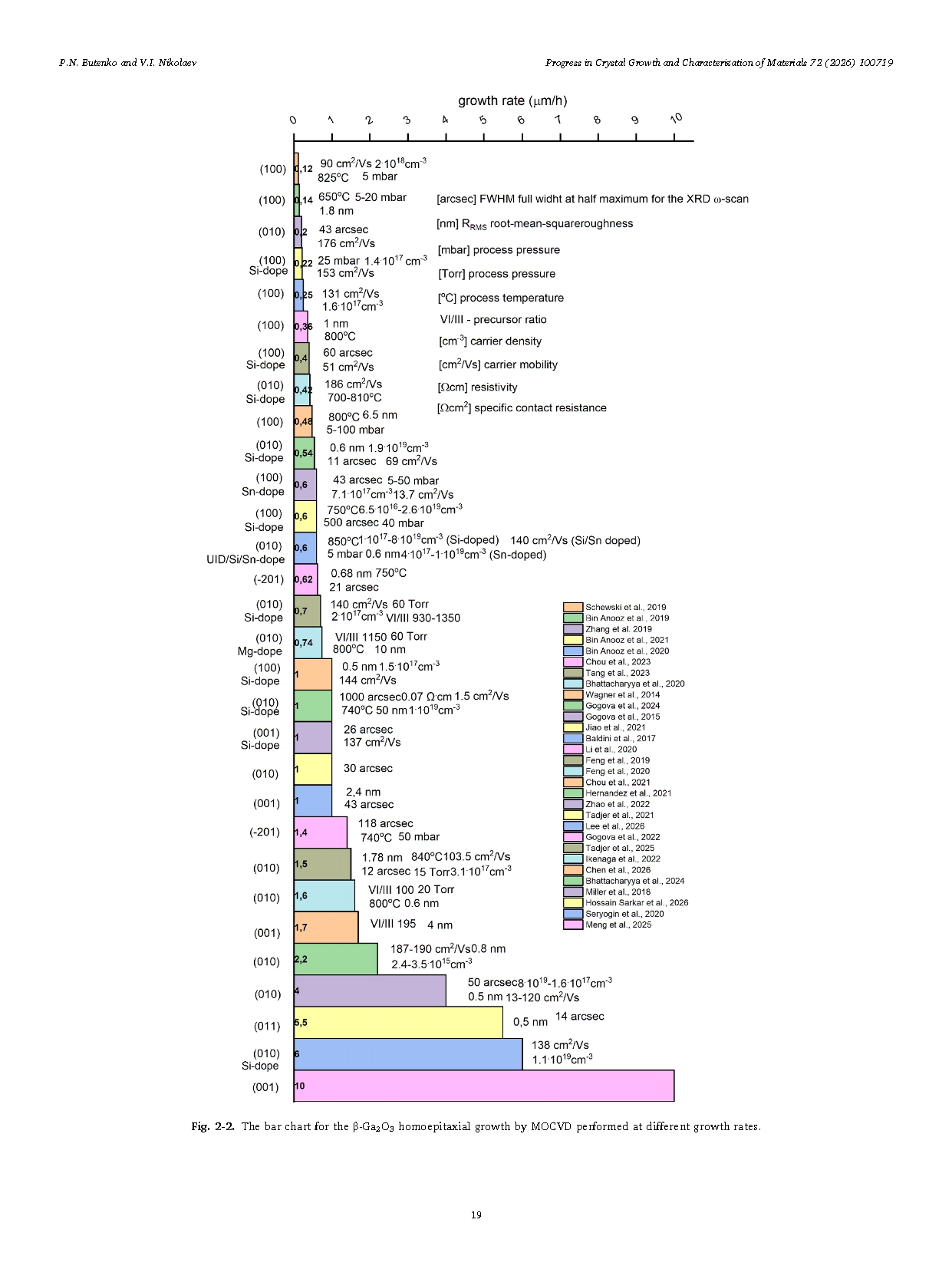
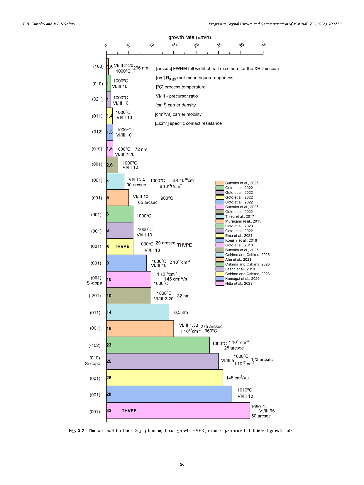
Based on surface energy evaluations, it can be argued that homoepitaxial growth on crystal planes which have higher Esurf demonstrate higher growth rates. This is consistent with Figs. 2-2, 3-2 and 4-2. Thus, the (010) and (201) β-Ga₂O₃ surfaces have preferential growth ability. Furthermore, the epitaxial layers grown on the former have the highest thermal conductivity, superior crystal perfection and low defect density, while the latter is the principal surface. In fact, the only restriction for [010] oriented wafers that can be encountered, is the limited area due to the specifics of EFG. Therefore, both are highly effective for growing high quality Ga₂O₃ homoepitaxial layers for power electronic applications. While the (100) and (001) substrates crystals, which are the cleavage planes and have low surface energy values, homoepitaxy on these planes can nevertheless demonstrate outperform results by applying miscut approach. Within the both of these substrates can have very large growth surfaces, application of miscut can allows for a step-flow mode to be achieved and inhibits the formation of twins and stacking faults. The serious issues for the [001]-oriented homoepitaxial layers are the emergence of rotational domains and a groove morphology within cracking along [010] direction. However, the latter problem can be solved to a significant extent by adjusting process parameters or introducing an In surfactant. In addition to the above orientations, (011) substrates should be mentioned, since they are recognized as the least defective of all conventional ones and as others are suitable for developing semiconductor devices.
Further, based, again, on Figs. 2-2, 3-2 and 4-2, it can be found that each CVD technique considered in this review, "prefers" a certain orientation. Thus, MOCVD utilizes (100) and (010) planes equally. It is clearly seen, that no homoepitaxial layers were grown on [100] oriented substrates with growth rates exceeding 1 μm/h by MOCVD. On the other hand, [010] and [201] oriented substrates always exhibit growth rates over this value. [001] orientation still owns moderate growth rate values, but it seems to have potential. However, it is the most often used for HVPE gallium oxide growth, despite the fact that homoepitaxial films grown by HVPE obviously contain variety of defects and it is occurred especially on (001) plane. The most often (010) is utilized for mist CVD homoepitaxial Ga₂O₃ growth. In some processes the films demonstrate high crystal perfection and very smooth morphology.
The analysis of the publications listed in this review, was aimed at confirming that CVD techniques are capable of fabricating high quality gallium oxide homoepitaxial layers. It can be argued that the latter will be efficient as layers for heterostructures, power electronics and optoelectronics. Thus, a composite layer configuration can be arranged, developing a controlled morphology with atomically flat surface. For those Ga₂O₃ crystal planes that suffer from high density of twin boundaries, stacking faults and other defects like threading dislocations, the defects can be suppressed in homoepitaxial layers. Finally, homoepitaxially fabricated layers should have higher crystal perfection, lower defects density, better homogeneity, lower surface roughness, than bulk crystals, have improved optoelectronic characteristics and be cheaper.
Thus, it can be confirmed, that each of the presented CVD growth techniques with the proper choice of the process parameters is fully responsible to improve the options listed above. With their help it is feasible to fabricate inexpensive epi-ready layers of a given thickness and shape possessing high crystal perfection and optoelectronic specifications. Based on the above, it is possible to predict in which areas these CVD methods may be most relevant for Ga₂O₃ growth. Thus, HVPE is highly prospective in fabricating thick buffer layers and quasi-bulk substrate crystals. MOCVD is a premium industrial technology for developing multilayer heterostructures. Mist CVD is a novel and cheap technology with a great potential.
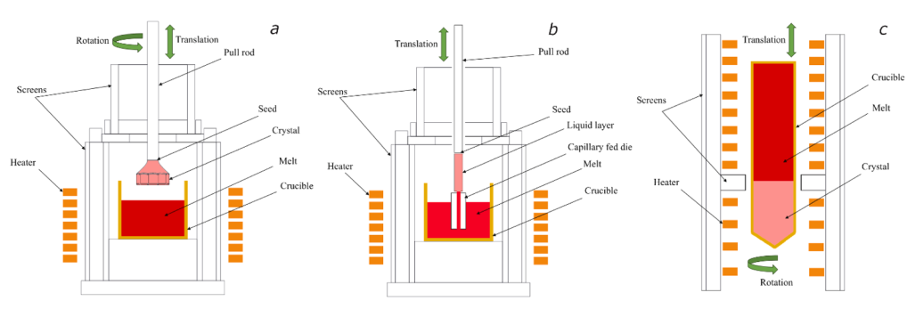
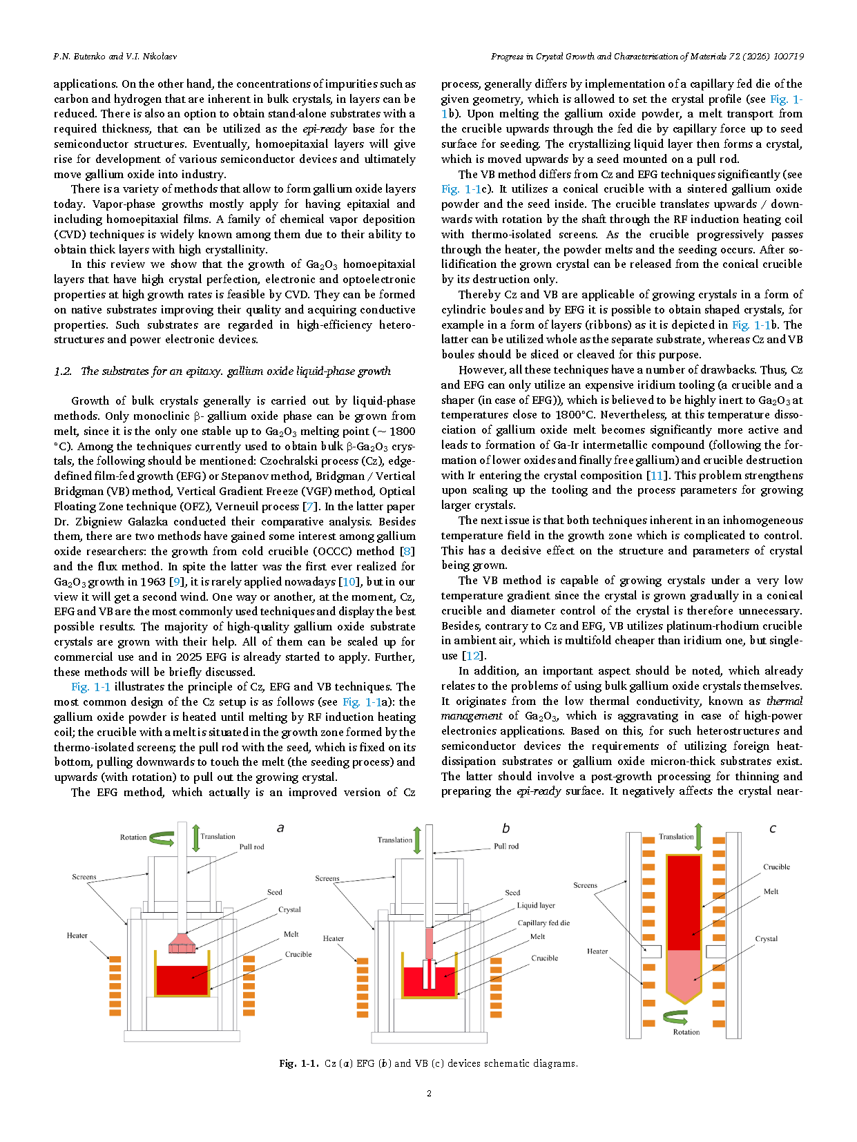
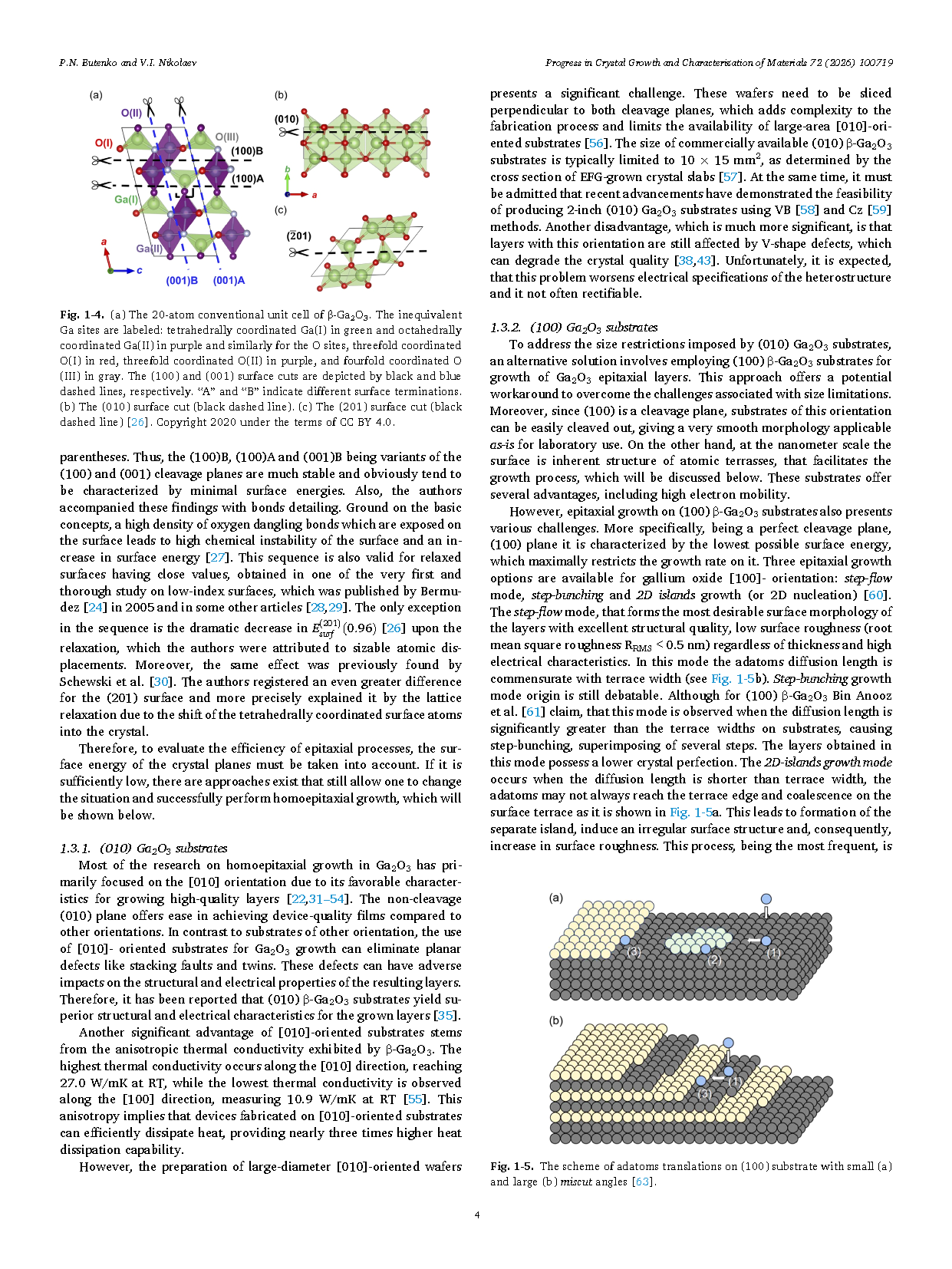
Fig. 1-1. Cz (a) EFG (b) and VB (c) devices schematic diagrams.
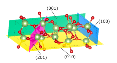
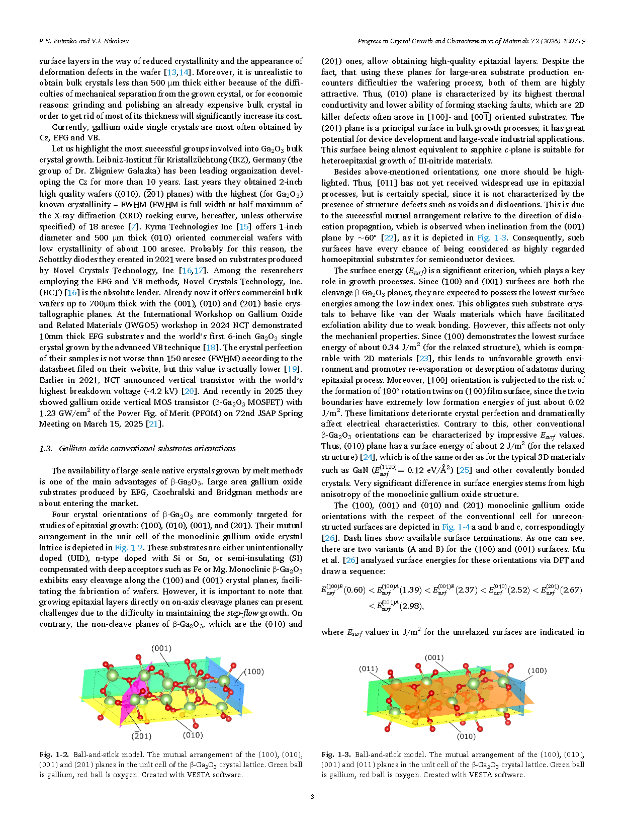
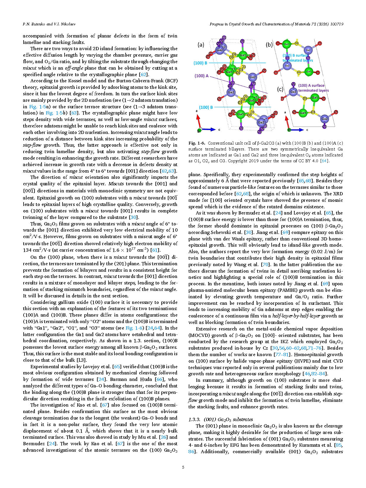
Fig. 1-2. Ball-and-stick model. The mutual arrangement of the (100), (010), (001) and (201) planes in the unit cell of the β-Ga₂O₃ crystal lattice. Green ball is gallium, red ball is oxygen. Created with VESTA software.
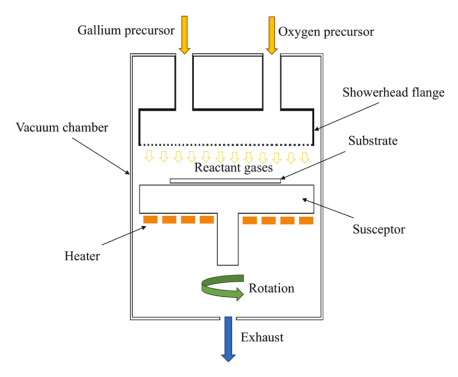
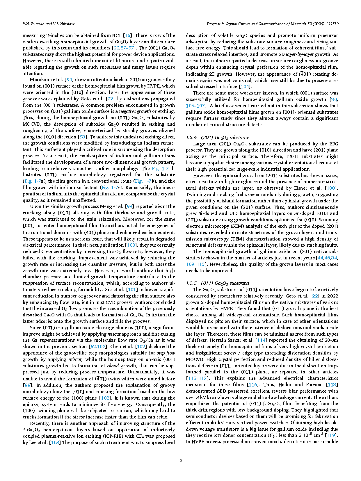
Fig. 2-1. Schematic diagram of MOCVD reactor for β-Ga₂O₃ epitaxial growth.
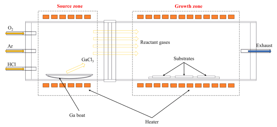
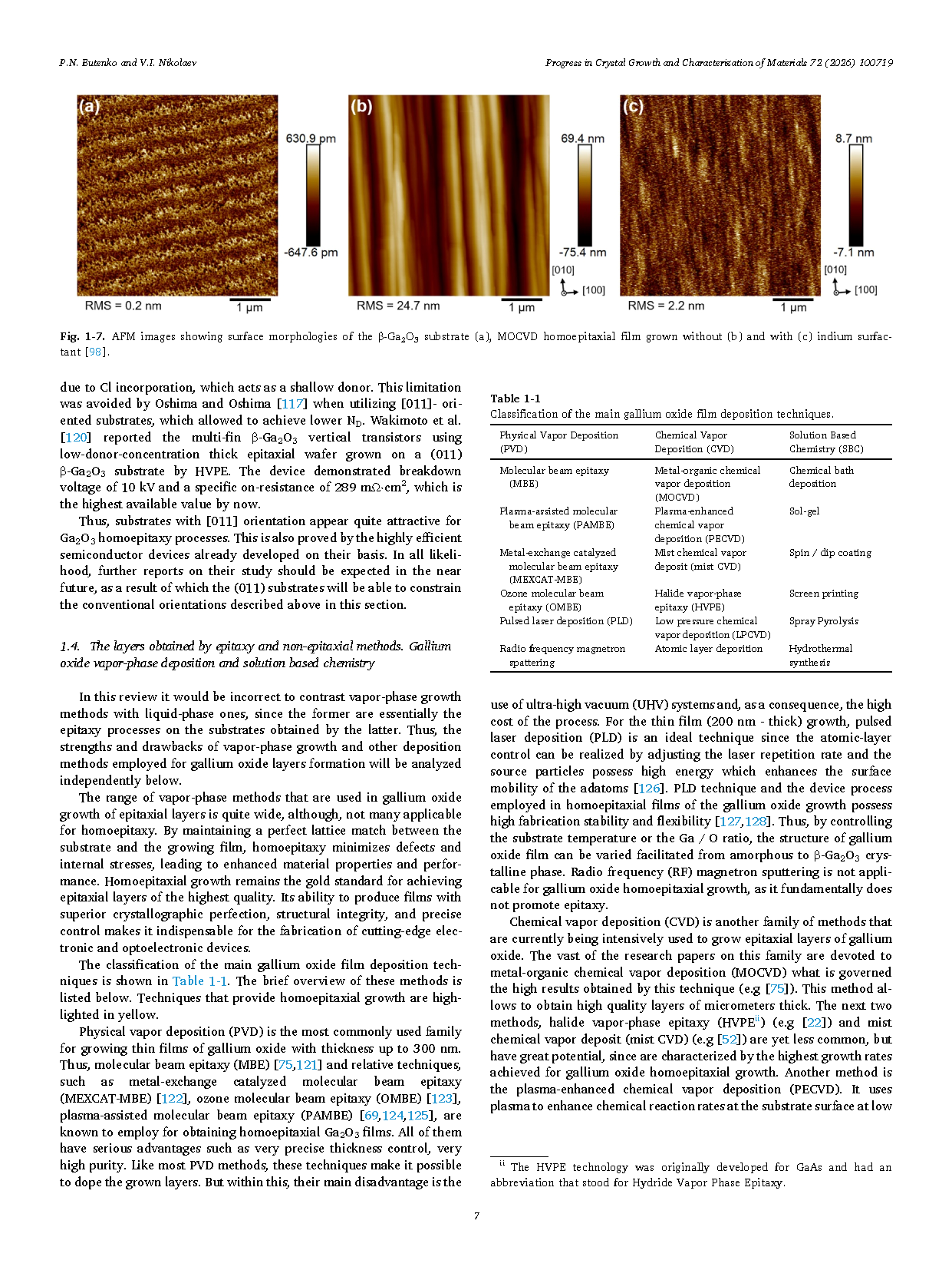
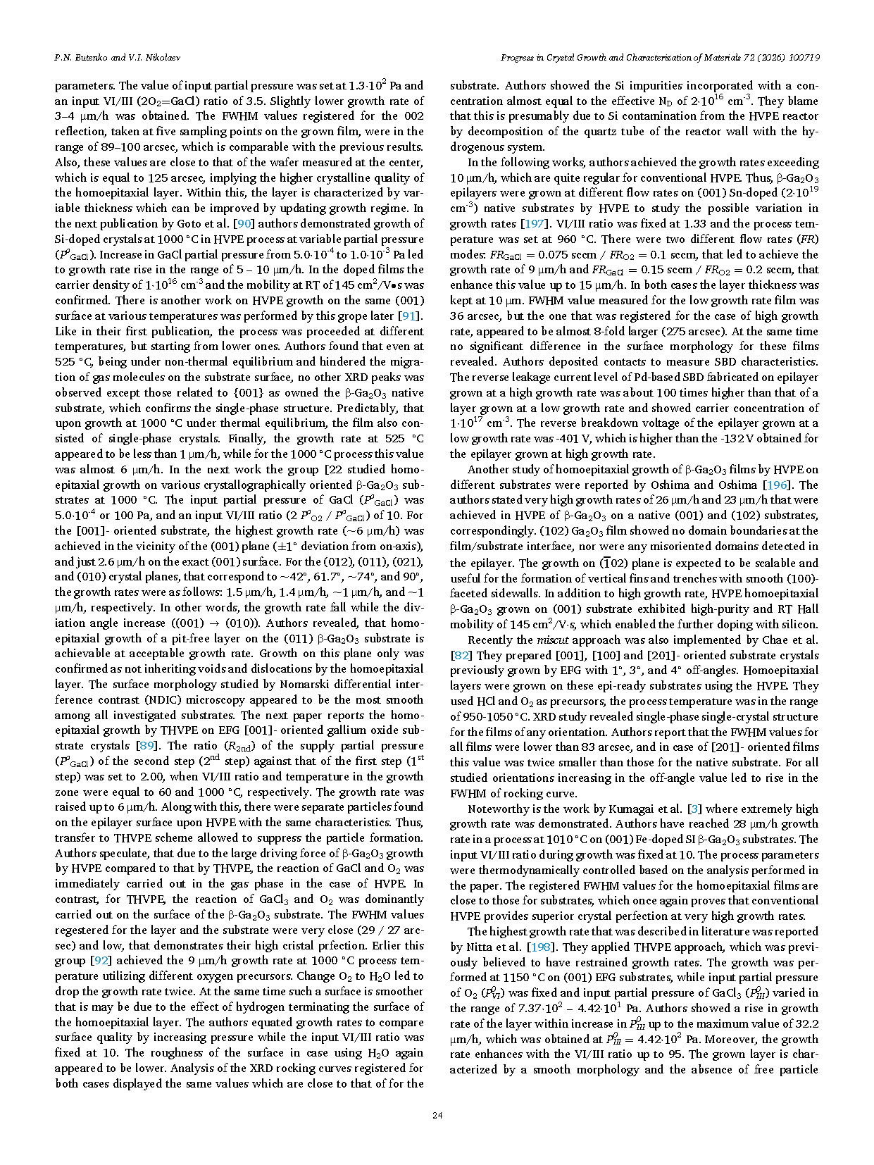
Fig. 3-1. Schematic of HVPE horizontal reactor for β-Ga₂O₃ epitaxial growth.
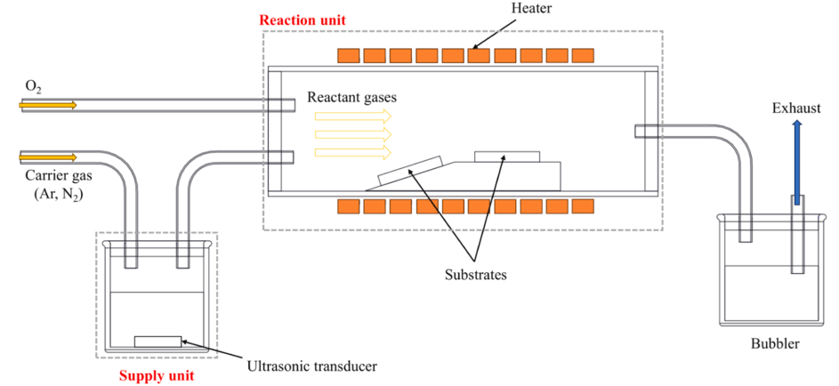
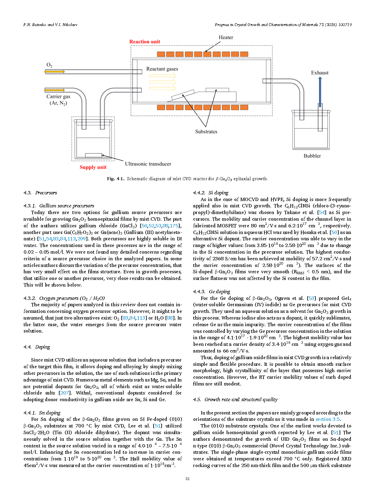
Fig. 4-1. Schematic diagram of mist CVD reactor for β-Ga₂O₃ epitaxial growth.
DOI:
doi.org/10.1016/j.pcrysgrow.2026.100719

Instruction
Official Account

Cooperation
Top
