


Researchers from Peter the Great St.-Petersburg Polytechnic University, Alferov University, JSC “Research and Production Enterprise ELAR”, University of Oslo have published a dissertation titled " Carrier removal in Ga₂O₃ polymorphs under ion irradiation " in Vacuum.
Background
Space nuclear reactors and high-energy accelerators require radiation-hard electronic devices. Ultra-wide bandgap Ga₂O₃ with bandgap of 4.6–5.3 eV is a promising candidate for space power chips and radiation sensors. Ion irradiation generates intrinsic defects and induces carrier removal, severely degrading device electrical performance. Most existing radiation researches only focus on β-Ga₂O₃ , while radiation-induced conductivity evolution in metastable α-Ga₂O₃ is poorly understood. There is no unified quantitative model to predict sheet resistance variation for both polymorphs under different ion species and irradiation temperatures. Previous works only provide qualitative analysis of defect accumulation, lacking universal theoretical framework to optimize ion implantation isolation technology, leaving an obvious research gap for radiation-resistant Ga₂O₃ device development.
Abstract
Irradiation-induced carrier removal is one of the major issues limiting utilization of materials in radiation-hard electronics. On the other hand, ion-beam-irradiation induced selective formation of highly resistive areas could be used for device isolation in electronic technology. Here we study the role of MeV light-ion irradiation on a conductivity evolution in α-Ga₂O₃ thin films. The results show that the dose dependence of sheet resistance exhibits a threshold-like behavior associated with decrease of free carrier concentration and lowering carrier mobility. The results can be adequately explained in the framework of a quantitative model based on the irradiation-induced formation of “defect-shallow dopant” complexes. Moreover, to prove the validity and versatility of used approaches, this model was successfully applied for the results of conductivity degradation in β-Ga₂O₃ irradiated with different ions. The obtained results can be used for better understanding radiation phenomena in Ga₂O₃ polymorphs paving the way for improvement of implant technology in Ga₂O₃ -based devices and development of radiation-tolerant electronic devices.
Highlights
Systematically investigate the conductivity degradation behavior of α-Ga₂O₃ thin films under 0.35 MeV He ion irradiation.
Propose a universal quantitative model based on defect-shallow dopant complex formation to describe threshold-type sheet resistance rising trend.
Verify the model universality via β-Ga₂O₃ samples irradiated by carbon and silicon ions at different temperatures.
Reveal the dominant compensation defects (gallium vacancy complexes) responsible for carrier removal in Ga₂O₃ polymorphs.
Conclusion
In conclusion, we study a conductivity evolution in α-Ga₂O₃ thin films under MeV light ion irradiation. A threshold-like behavior of sheet resistance as a function of ion dose was observed that is associated to decrease of the free carrier concentration and lowering carrier mobility. Furthermore, the carrier removal rate is maximal for low doses and exhibits lowering trend with increasing ion dose. We demonstrate that the observed carrier removal trends in the irradiated α-Ga₂O₃ can be adequately explained in the framework of the model based on the irradiation-induced formation of "defect-shallow donor" complexes. Moreover, to prove the validity and versatility of used approaches, this model was applied for the results obtained for irradiated β-Ga₂O₃ . The obtained results can be used for better understanding radiation phenomena in Ga₂O₃ polymorphs paving the way for improvement of implant technology in Ga₂O₃ -based devices and development of radiation-tolerant electronic devices.
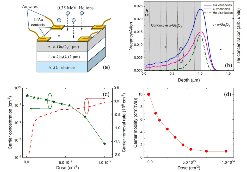
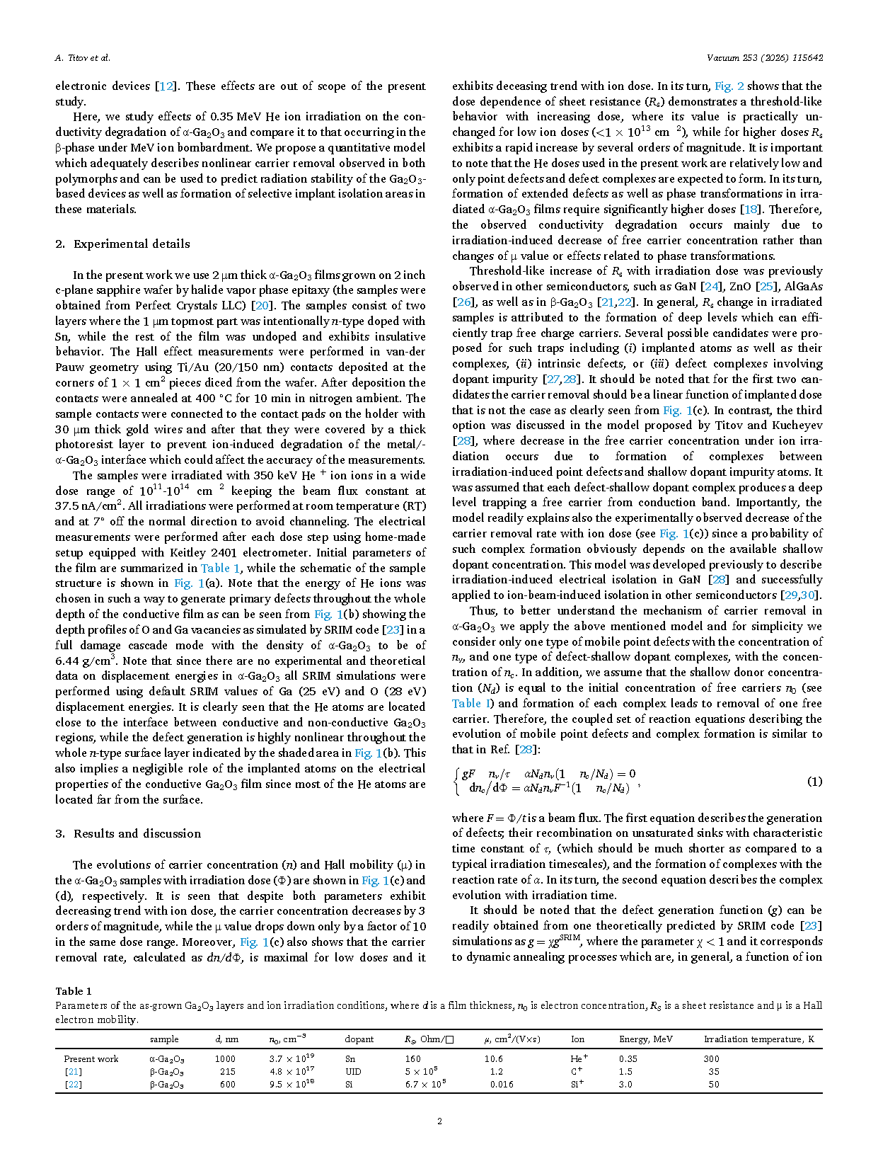
Fig. 1. (a) Schematic of the sample structure, (b) point defect (vacancy) generation function in α-Ga₂O₃ as predicted by SRIM code [23] simulations for 0.35 MeV He⁺ irradiation. (c) Carrier concentration (left-hand-side scale) as well as carrier removal rate (right-hand-side scale) and (d) Hall electron mobility in α-Ga₂O₃ layer as a function of irradiation dose.
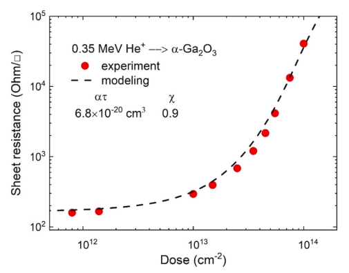
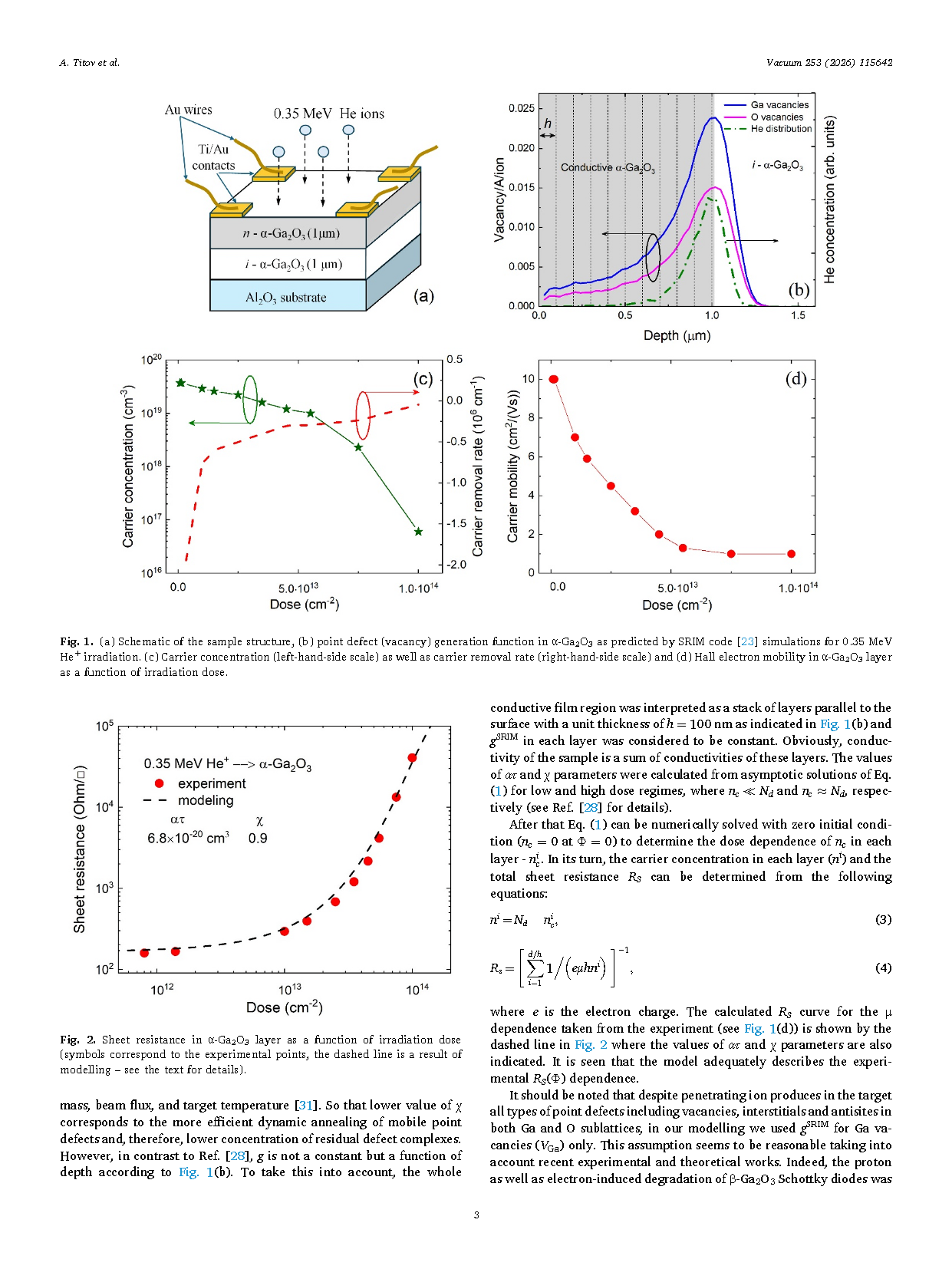
Fig. 2. Sheet resistance in α-Ga₂O₃ layer as a function of irradiation dose (symbols correspond to the experimental points, the dashed line is a result of modelling – see the text for details).
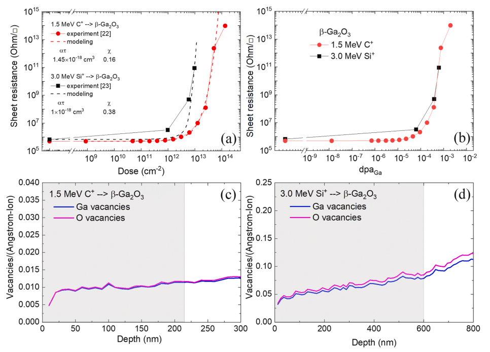
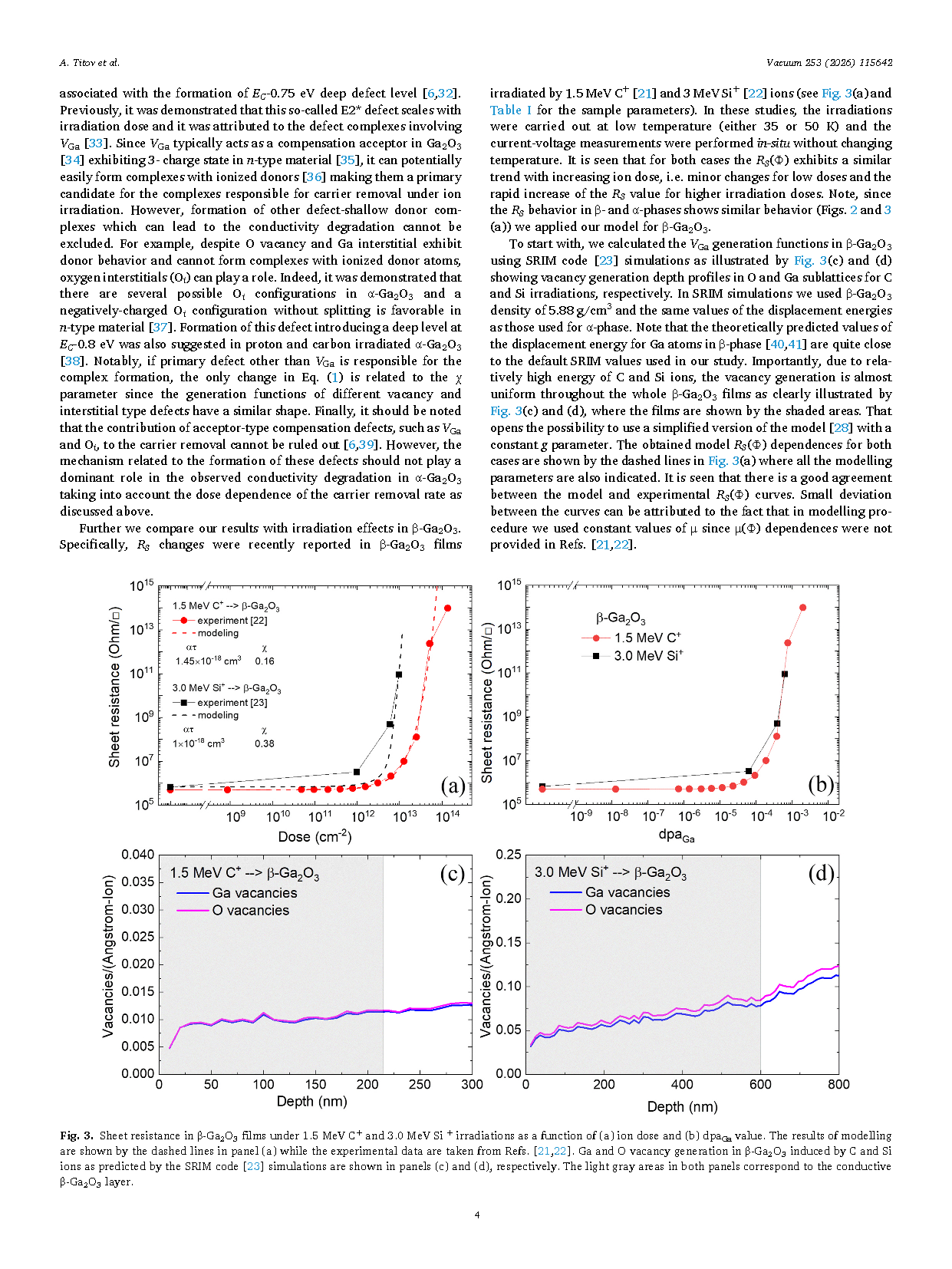
Fig. 3. Sheet resistance in β-Ga₂O₃ films under 1.5 MeV C⁺ and 3.0 MeV Si⁺ irradiations as a function of (a) ion dose and (b) dpa_Ga value. The results of modelling are shown by the dashed lines in panel (a) while the experimental data are taken from Refs. [21,22]. Ga and O vacancy generation in β-Ga₂O₃ induced by C and Si ions as predicted by the SRIM code [23] simulations are shown in panels (c) and (d), respectively. The light gray areas in both panels correspond to the conductive β-Ga₂O₃ layer.
DOI:
doi.org/10.1016/j.vacuum.2026.115642
Instruction
Official Account

Cooperation
Top
