


Researchers from the Shandong University and Ningbo University of Technology and Ningbo University have published a dissertation titled " Complementary optoelectronic effect in silicon nanomembrane-based heterojunction for broadband UV–visible–NIR photodetection " in Applied Physics Letters.
Background
Photodetectors realize the sensing and analysis of optical signals via photoelectric conversion, possessing irreplaceable application value in optical communication, optical computing, biomedical imaging, security surveillance, aerospace, environmental monitoring and other fields. Among them, broadband photodetectors can simultaneously capture optical signals covering ultraviolet, visible and near-infrared bands, and support complex detection scenarios including material composition analysis, remote geological exploration, marine ecological monitoring and military target identification, which act as fundamental components of advanced optical systems and have become a key research hotspot in optoelectronics in recent years.
Single silicon-based photodetectors only respond to visible to near-infrared light (400–1100 nm) and fail to detect solar-blind ultraviolet radiation. In UV region, silicon exhibits extremely high light absorption coefficient with photon penetration depth less than tens of nanometers. Besides, silicon has large reflectivity and limited carrier lifetime under UV illumination, which severely degrade its UV photodetection performance. Gallium oxide (Ga₂O₃) is an ultra-wide bandgap semiconductor with bandgap of 4.5–5.2 eV and outstanding capacity for solar-blind UV (200–280 nm) detection, making it a promising candidate for UV photodetectors.
Constructing Ga₂O₃/Si heterojunctions can theoretically realize full-spectrum broadband photodetection covering UV–visible–NIR bands. Nevertheless, existing fabrication routes face prominent drawbacks. Heterojunctions fabricated by transfer printing require elaborate structural design of silicon thin films, and large-area manufacturing is challenging. Epitaxial growth of Ga₂O₃ on silicon substrates introduces high dislocation density and residual stress originating from severe lattice and thermal expansion mismatch, accompanied by long epitaxy duration that restricts mass production. Accordingly, a facile, scalable fabrication strategy for Ga₂O₃/Si heterojunctions is urgently required.
Abstract
Semiconductor heterojunctions play a vital role in the fabrication of broadband photodetectors, which offer broad application prospects across fields including environmental monitoring, biomedical imaging, and optical communications. However, state-of-the-art technical routes for the fabrication of semiconductor heterojunctions face significant challenges, which could severely compromise their optoelectronic properties. Here, we report a simple and convenient approach for the fabrication of semiconductor heterojunctions, which contains silicon nanomembranes and liquid metal printed gallium oxide. Large-area gallium oxide with controllable thickness can be formed on the top of silicon nanomembranes through spontaneous oxidation of printed liquid gallium. Facilitated by the complementary optoelectronic effects, various light sources with wavelengths covering the solar blind, visible, and near-infrared bands could effectively activate electron–hole pairs in the depletion region of the heterojunction, which can be further separated by the built-in potential. Therefore, the fabricated photodetector exhibits high optoelectronic performances, including broadband photodetection (255–980 nm), high responsivity (3.18 A/W), and detectivity (1.0 ×10¹³ Jones), good stability, fast response time (8/10 ms), and self-powered capability. This work adds to the portfolio of material strategies and fabrication process in high-performance, large-area broadband photodetection platforms.
Highlights
①A facile liquid gallium printing strategy is developed to fabricate wafer-scale Ga₂O₃/Si nanomembrane heterojunctions; continuous large-area Ga₂O₃ films with tunable thickness are formed via spontaneous oxidation of liquid Ga.
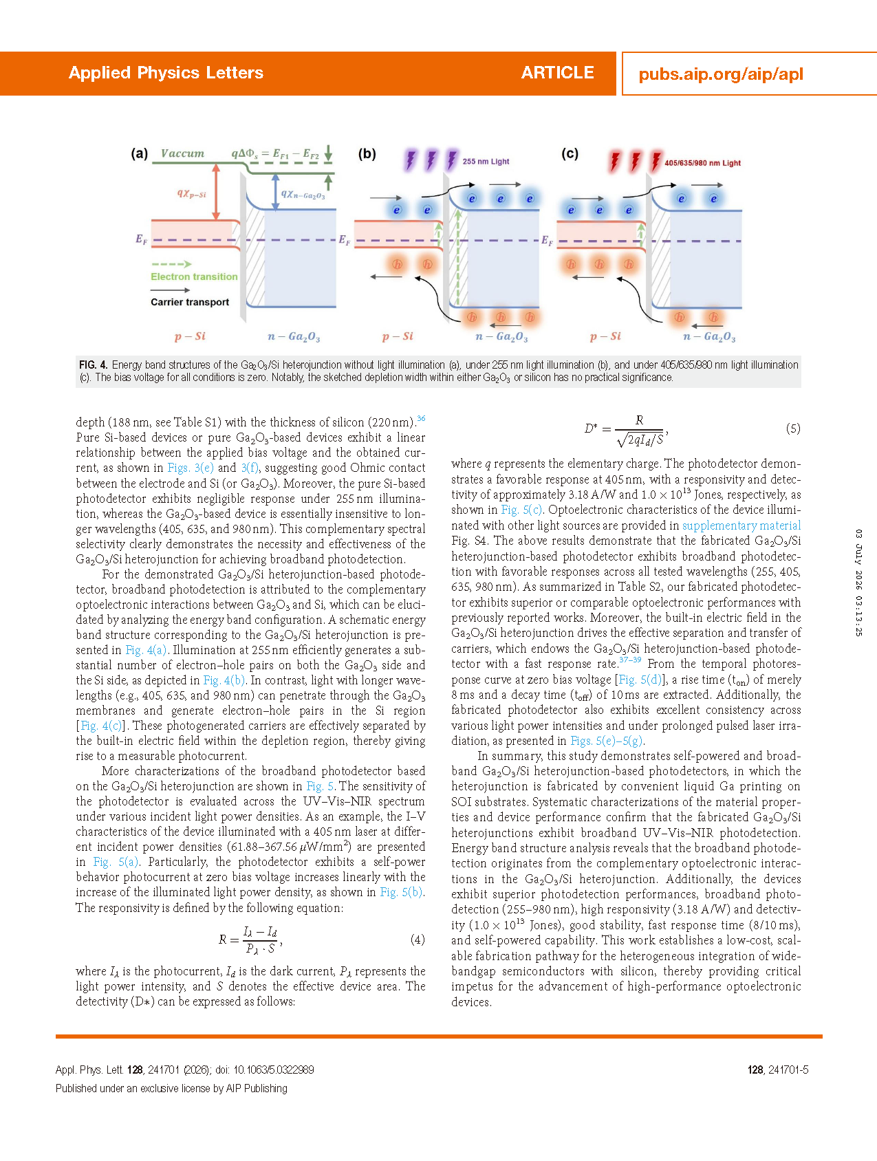
②Complementary optoelectronic effect is revealed in Ga₂O₃/Si PN heterojunction: solar-blind UV light generates carriers in Ga₂O₃, while visible/NIR light penetrates Ga₂O₃ and excites electron-hole pairs in silicon nanomembranes, enabling full-spectrum photodetection (255–980 nm).
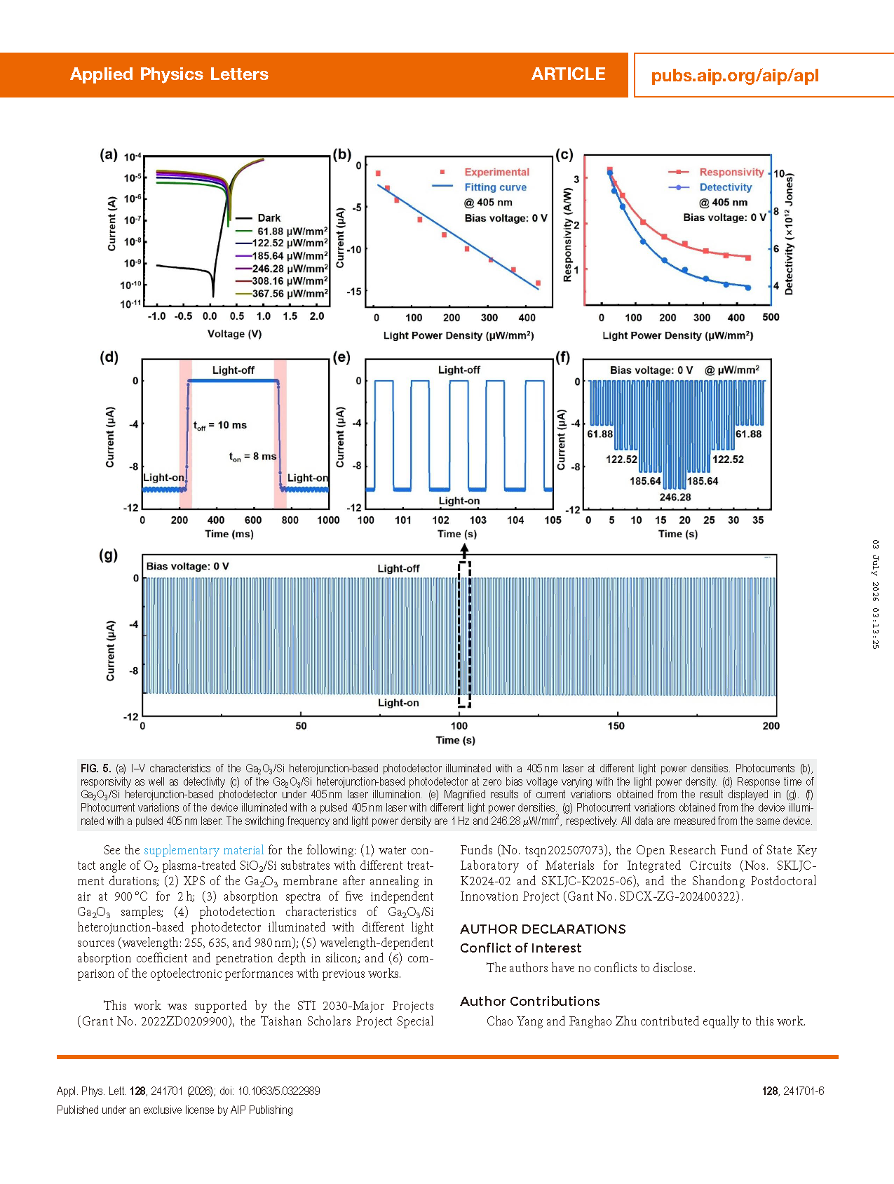
③The self-powered broadband photodetector achieves superior optoelectronic performance: high responsivity of 3.18 A/W, detectivity up to 1.0 ×10¹³ Jones, fast rise/decay time of 8 ms/10 ms and outstanding long-term stability.
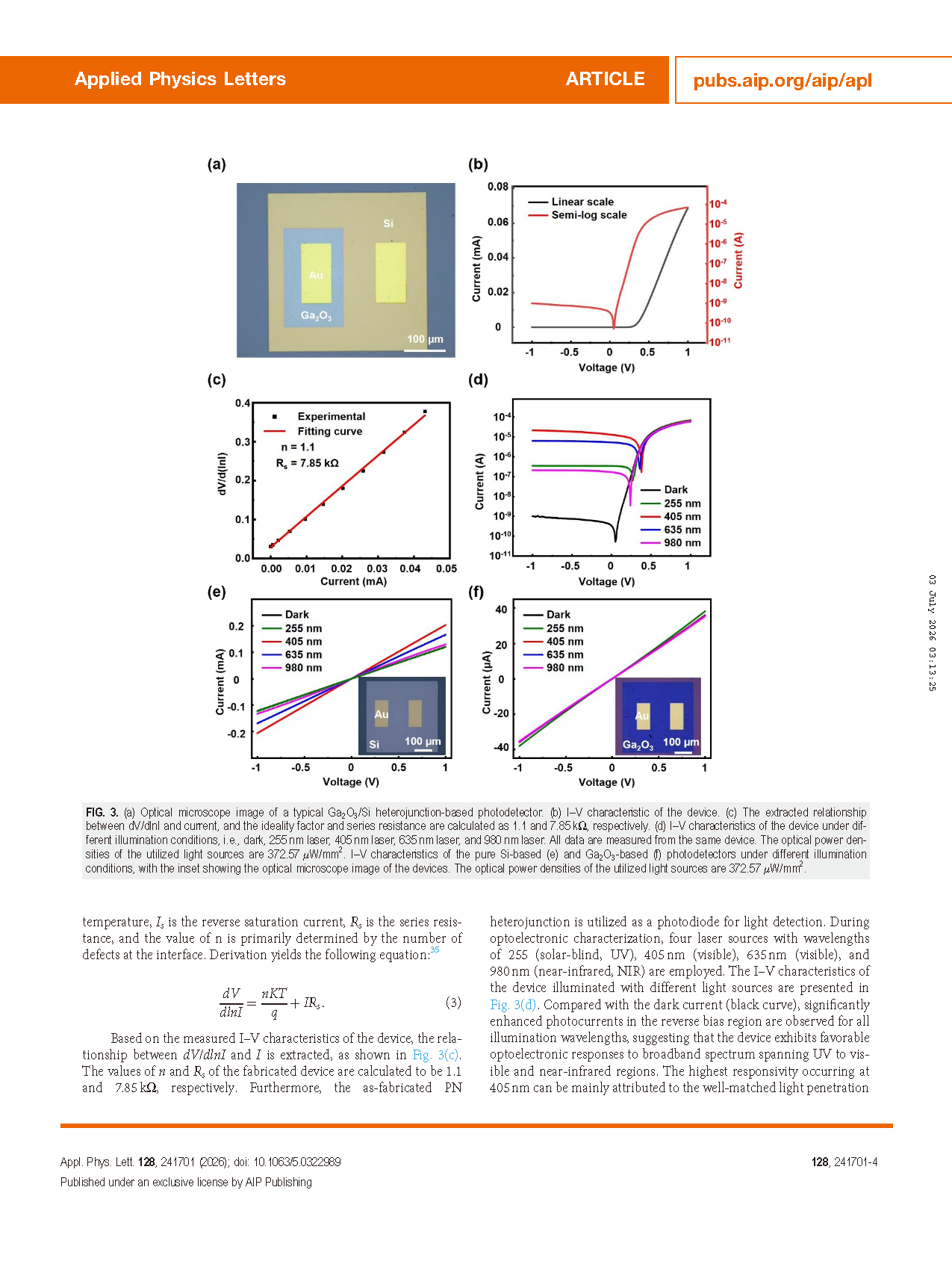
④Post-annealing at 270 °C in air eliminates residual metallic Ga and reduces oxygen vacancies; the heterojunction exhibits ideal rectification behavior with ideality factor n=1.1 and low interface defects.
Conclusion
In summary, this study demonstrates self-powered and broadband Ga₂O₃/Si heterojunction-based photodetectors, in which the heterojunction is fabricated by convenient liquid Ga printing on SOI substrates. Systematic characterizations of the material properties and device performance confirm that the fabricated Ga₂O₃ heterojunctions exhibit broadband UV–Vis–NIR photodetection. Energy band structure analysis reveals that the broadband photodetection originates from the complementary optoelectronic interactions in the Ga₂O₃/Si heterojunction. Additionally, the devices exhibit superior photodetection performances, broadband photodetection (255–980 nm), high responsivity (3.18 A/W) and detectivity (1.0 ×10¹³ Jones), good stability, fast response time (8/10 ms), and self-powered capability. This work establishes a low-cost, scalable fabrication pathway for the heterogeneous integration of wide-bandgap semiconductors with silicon, thereby providing critical impetus for the advancement of high-performance optoelectronic devices.
Project Support
This work was supported by the STI 2030-Major Projects (Grant No. 2022ZD0209900), the Taishan Scholars Project Special Funds (No. tsqn202507073), the Open Research Fund of State Key Laboratory of Materials for Integrated Circuits (Nos. SKLJC-K2024-02 and SKLJC-K2025-06), and the Shandong Postdoctoral Innovation Project (Grant No. SDCX-ZG-202400322).
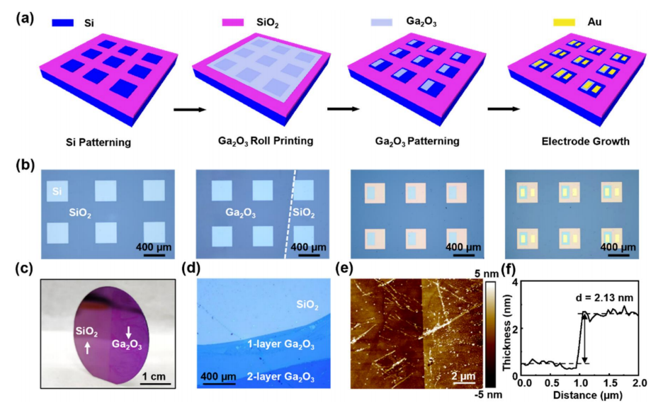
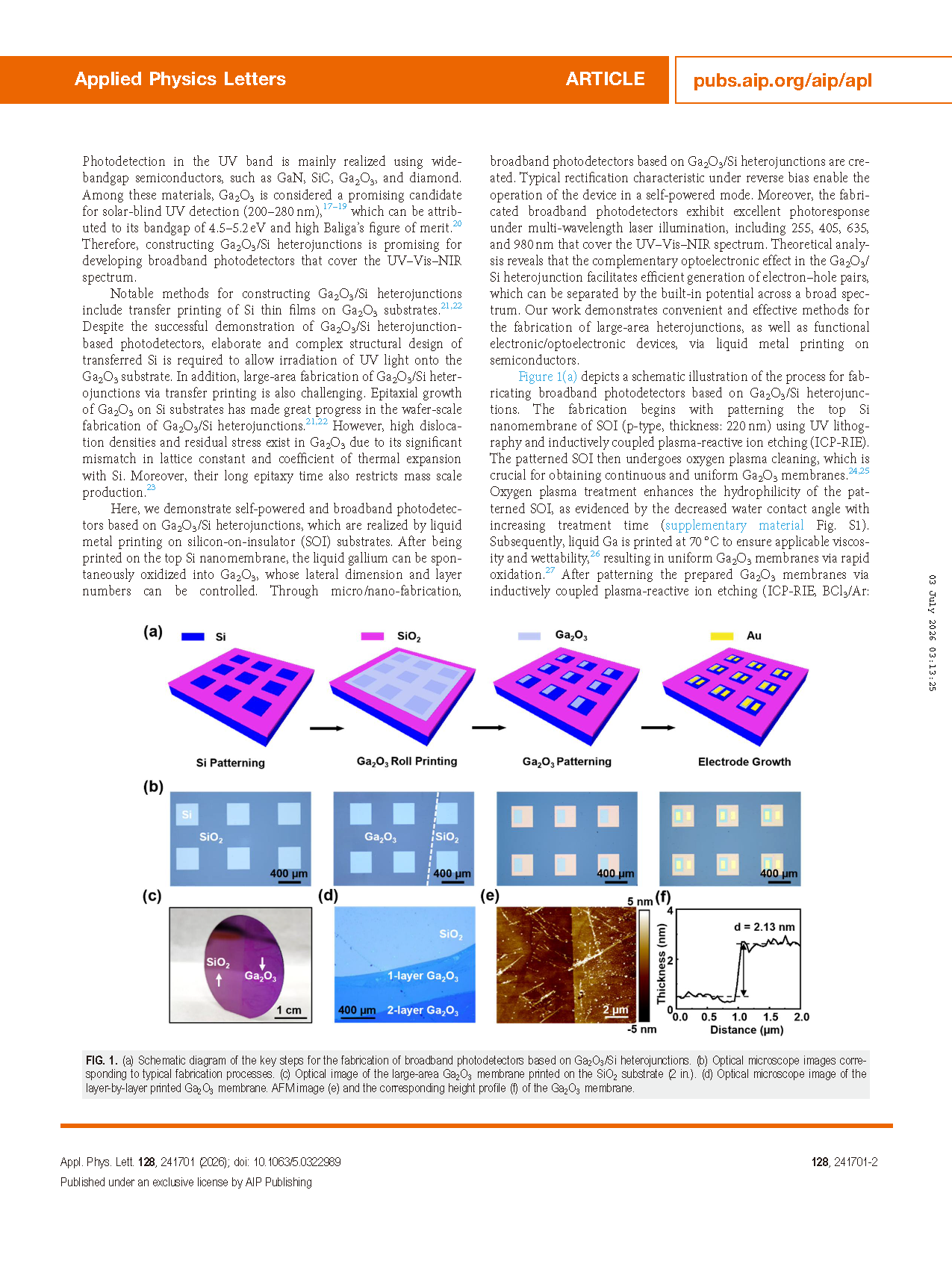
Fig. 1. (a) Schematic diagram of the key steps for the fabrication of broadband photodetectors based on Ga₂O₃/Si heterojunctions. (b) Optical microscope images corresponding to typical fabrication processes. (c) Optical image of the large-area Ga₂O₃ membrane printed on the SiO₂ substrate (2 in.). (d) Optical microscope image of the layer-by-layer printed Ga₂O₃ membrane. AFM image (e) and the corresponding height profile (f) of the Ga₂O₃ membrane.
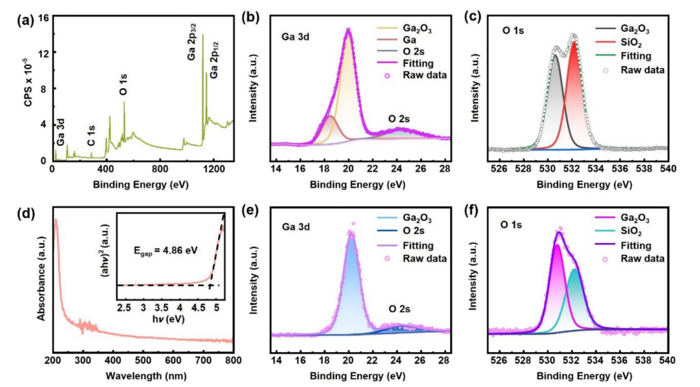
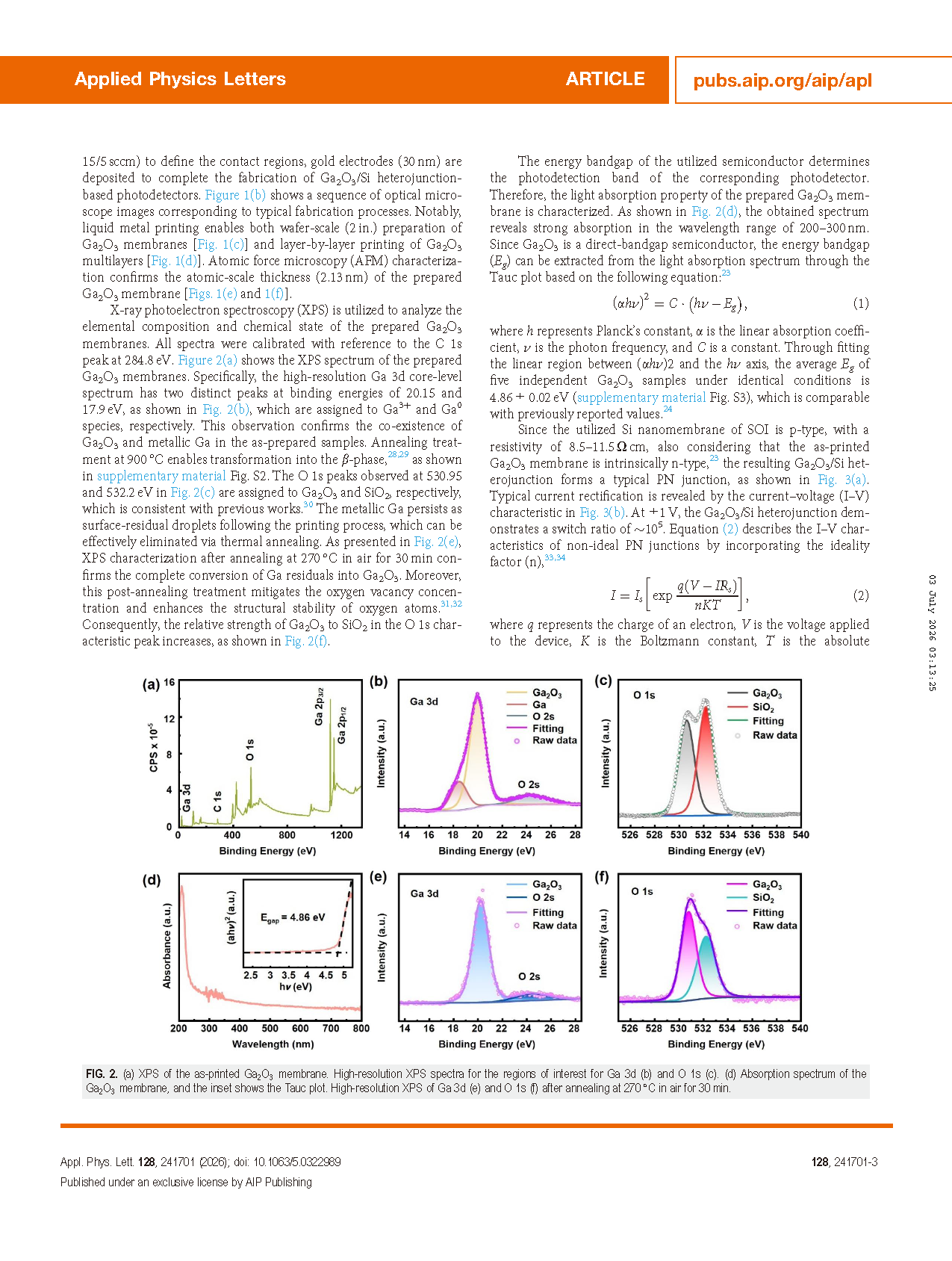
Fig. 2. (a) XPS of the as-printed Ga₂O₃ membrane. High-resolution XPS spectra for the regions of interest for Ga 3d (b) and O 1s (c). (d) Absorption spectrum of the Ga₂O₃ membrane, and the inset shows the Tauc plot. High-resolution XPS of Ga 3d (e) and O 1s (f) after annealing at 270 °C in air for 30 min.
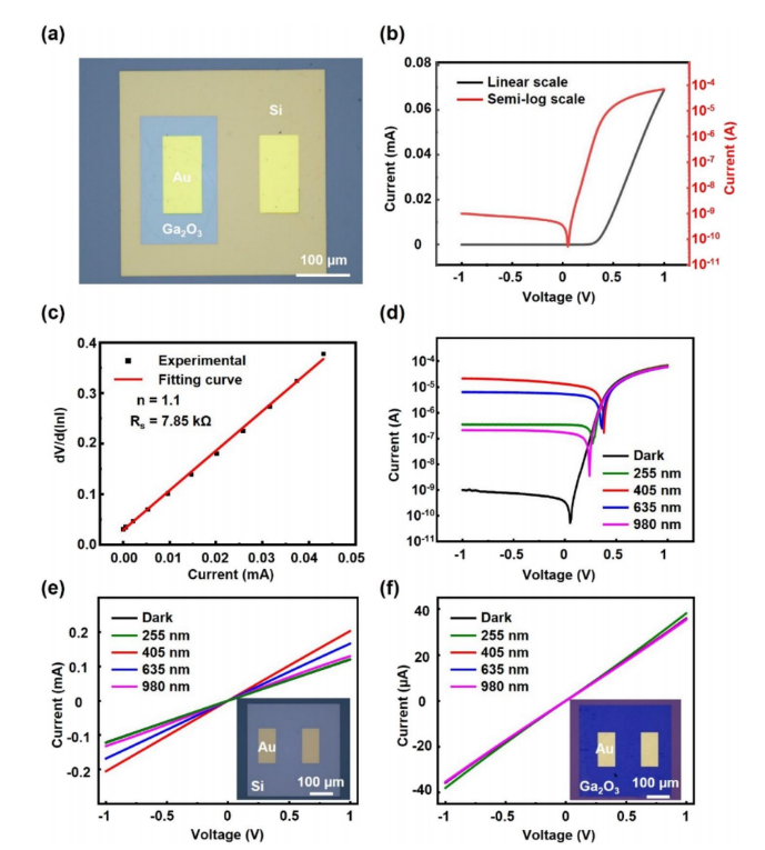
Fig. 3. (a) Optical microscope image of a typical Ga₂O₃/Si heterojunction-based photodetector. (b) I–V characteristic of the device. (c) The extracted relationship between dV/dlnI and current, and the ideality factor and series resistance are calculated as 1.1 and 7.85 kΩ, respectively. (d) I–V characteristics of the device under different illumination conditions, i.e., dark, 255 nm laser, 405 nm laser, 635 nm laser, and 980 nm laser. All data are measured from the same device. The optical power densities of the utilized light sources are 372.57 μW/mm². I–V characteristics of the pure Si-based (e) and Ga₂O₃-based (f) photodetectors under different illumination conditions, with the inset showing the optical microscope image of the devices. The optical power densities of the utilized light sources are 372.57 μW/mm².
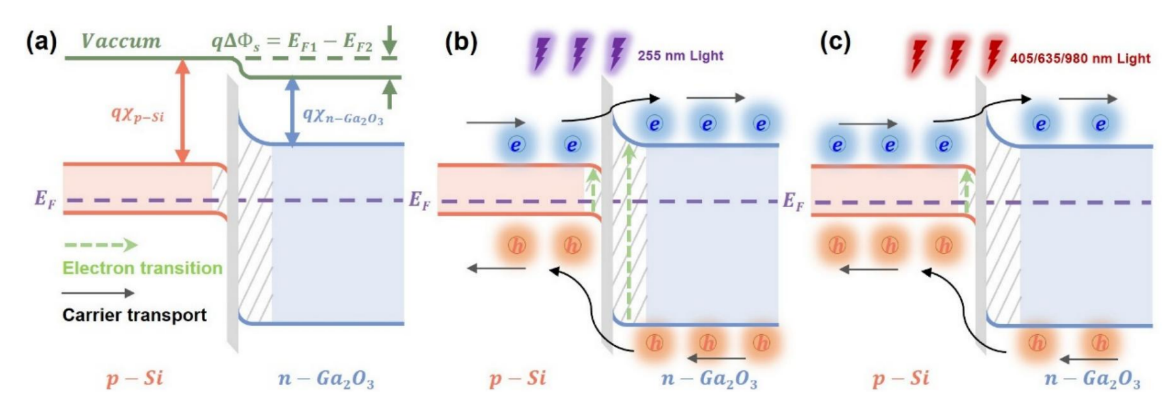
Fig. 4. Energy band structures of the Ga₂O₃/Si heterojunction without light illumination (a), under 255 nm light illumination (b), and under 405/635/980 nm light illumination (c). The bias voltage for all conditions is zero. Notably, the sketched depletion width within either Ga₂O₃ or silicon has no practical significance.
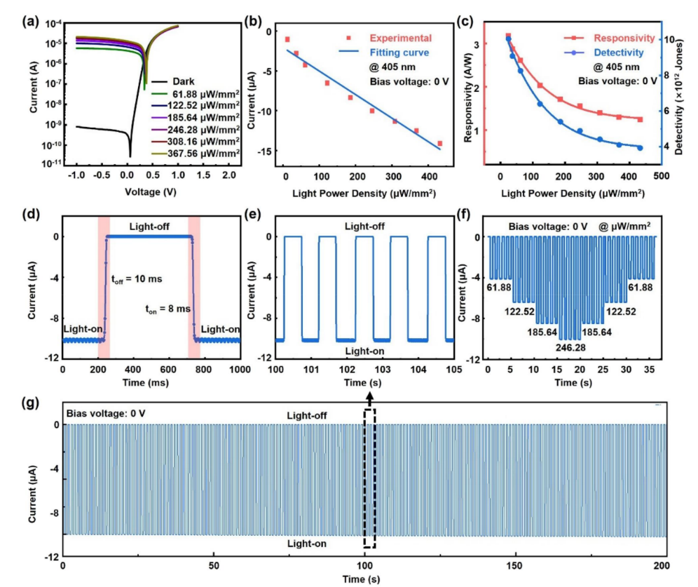
Fig. 5. (a) I–V characteristics of the Ga₂O₃/Si heterojunction-based photodetector illuminated with a 405 nm laser at different light power densities. Photocurrents (b), responsivity as well as detectivity (c) of the Ga₂O₃/Si heterojunction-based photodetector at zero bias voltage varying with the light power density. (d) Response time of Ga₂O₃/Si heterojunction-based photodetector under 405 nm laser illumination. (e) Magnified results of current variations obtained from the result displayed in (g). (f) Photocurrent variations of the device illuminated with a pulsed 405 nm laser with different light power densities. (g) Photocurrent variations obtained from the device illuminated with a pulsed 405 nm laser. The switching frequency and light power density are 1 Hz and 246.28 μW/mm², respectively. All data are measured from the same device.
DOI :
10.1063/5.0322989
Instruction
Official Account

Cooperation
Top
