


Researchers from University of Science and Technology of China have published a dissertation titled " Over 3.5 kV (011) β-Ga₂O₃ Schottky Barrier Diode and First Demonstration of 4.7 kV NiO-based (011) β-Ga₂O₃ Heterojunction Diode " in 2026 IEEE 38th International Symposium on Power Semiconductor Devices and ICs (ISPSD).
Background
Ultra-wide bandgap semiconductor Gallium oxide (β Ga₂O₃) has been the hot topic of power devices recent years, due to its wide bandgap (4.5~4.8 eV), high breakdown electric field of 6~8 MV/cm, controllable n-type doping and large-area wafer availability. Owing to these excellent material properties, β-Ga₂O₃ has emerged as a promising candidate for high-voltage applications (>3300 V), such as high-voltage direct current transmission systems, rail transportation and new energy power generation, to reduce energy loss and improve efficiency.
Abstract
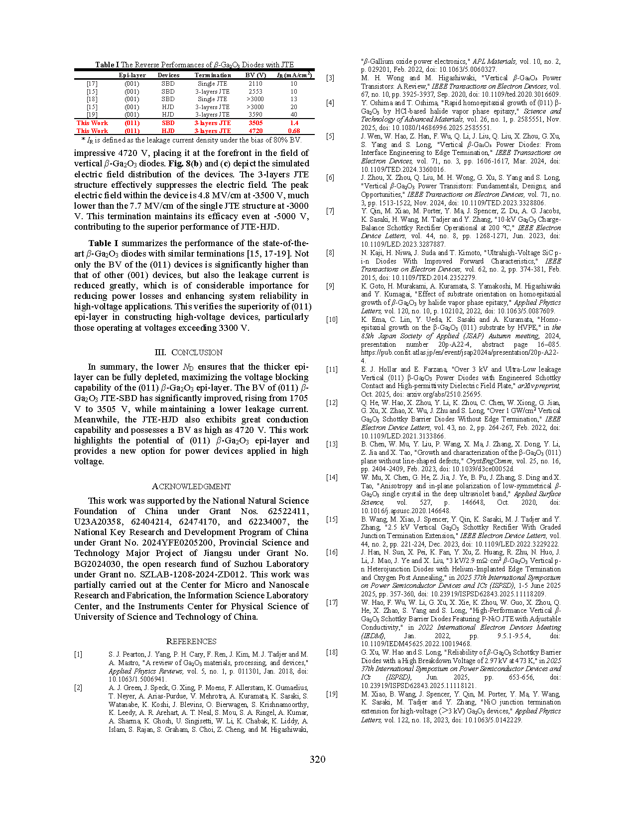
The superior material properties of β-Ga₂O₃ make it a promising candidate for high-voltage applications. High quality epi-layers are essential for power devices to enhance the breakdown voltage (BV). However, the widely used (001) β-Ga₂O₃ epi-layer encounters challenges in increasing thickness and reducing carrier concentration, which limits the further improvement of the BV. Importantly, the (011) β-Ga₂O₃ epi-layer does not suffer from these bottlenecks. In this work, we compared the characteristics of Schottky barrier diodes (SBDs) based on (011) and (001) epi-layers. Owing to the fully depleted epi-layer, the BV of (011) SBD without termination reached 1785 V, which is significantly higher than that of (001) SBD. Furthermore, we demonstrated the first NiO-based heterojunction diode (HJD) on (011) β-Ga₂O₃ epi-layer. By utilizing a 3-layers junction termination extension structure, the BV of SBD and HJD improved to 3505 V and 4720 V respectively, confirming the superiority of (011) epi-layer in constructing high-voltage devices.
Conclusion
In summary, the lower ND ensures that the thicker epi layer can be fully depleted, maximizing the voltage blocking capability of the (011) β-Ga₂O₃ epi-layer. The BV of (011) β Ga₂O₃ JTE-SBD has significantly improved, rising from 1705 V to 3505 V, while maintaining a lower leakage current. Meanwhile, the JTE-HJD also exhibits great conduction capability and possesses a BV as high as 4720 V. This work highlights the potential of (011) β-Ga₂O₃ epi-layer and provides a new option for power devices applied in high voltage.
Project Support
This work was supported by the National Natural Science Foundation of China under Grant Nos. 62522411, U23A20358, 62404214, 62474170, and 62234007, the National Key Research and Development Program of China under Grant No. 2024YFE0205200, Provincial Science and Technology Major Project of Jiangsu under Grant No. BG2024030, the open research fund of Suzhou Laboratory under Grant no. SZLAB-1208-2024-ZD012. This work was partially carried out at the Center for Micro and Nanoscale Research and Fabrication, the Information Science Laboratory Center, and the Instruments Center for Physical Science of University of Science and Technology of China.
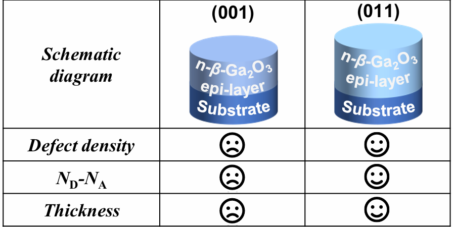
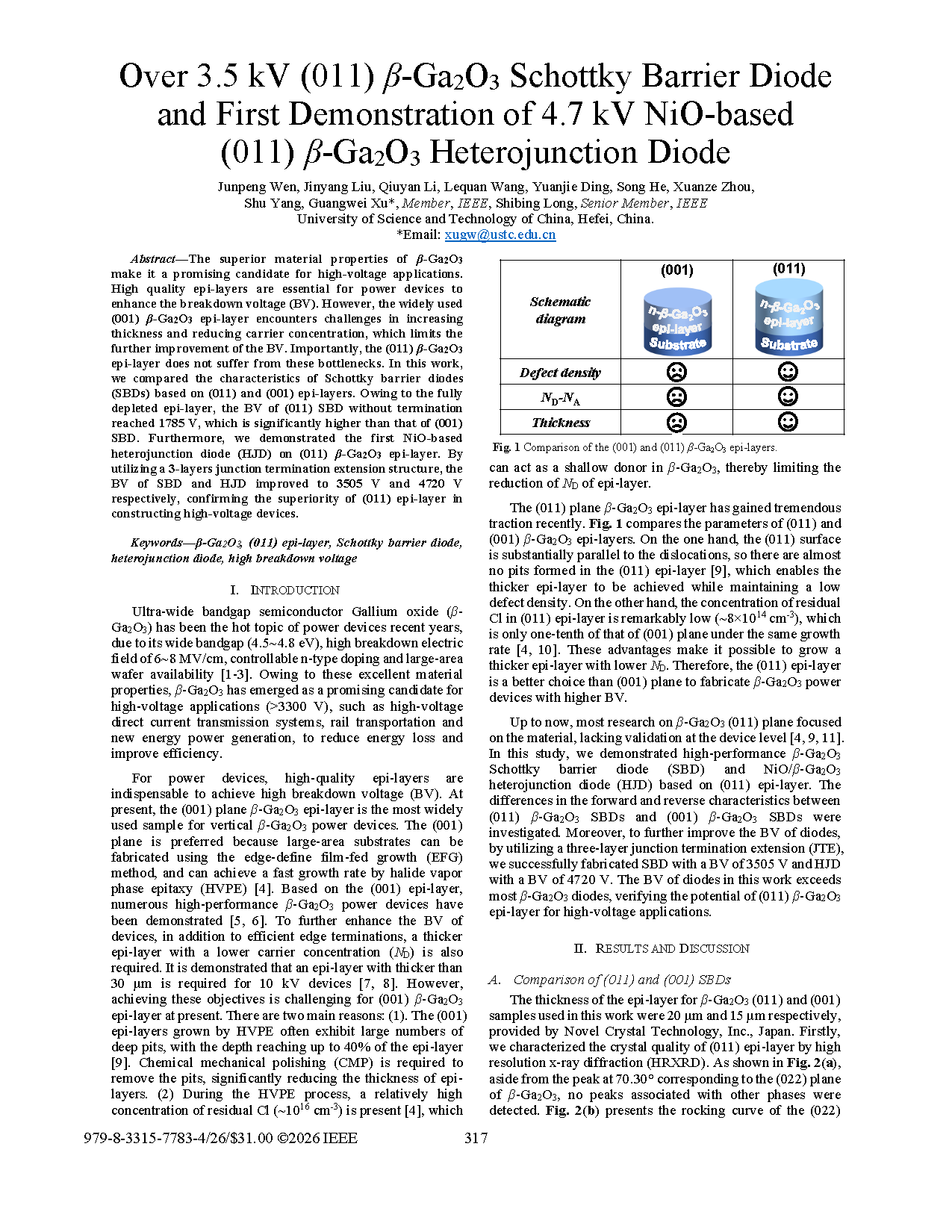
Fig. 1 Comparison of the (001) and (011) β-Ga₂O₃ epi-layers.
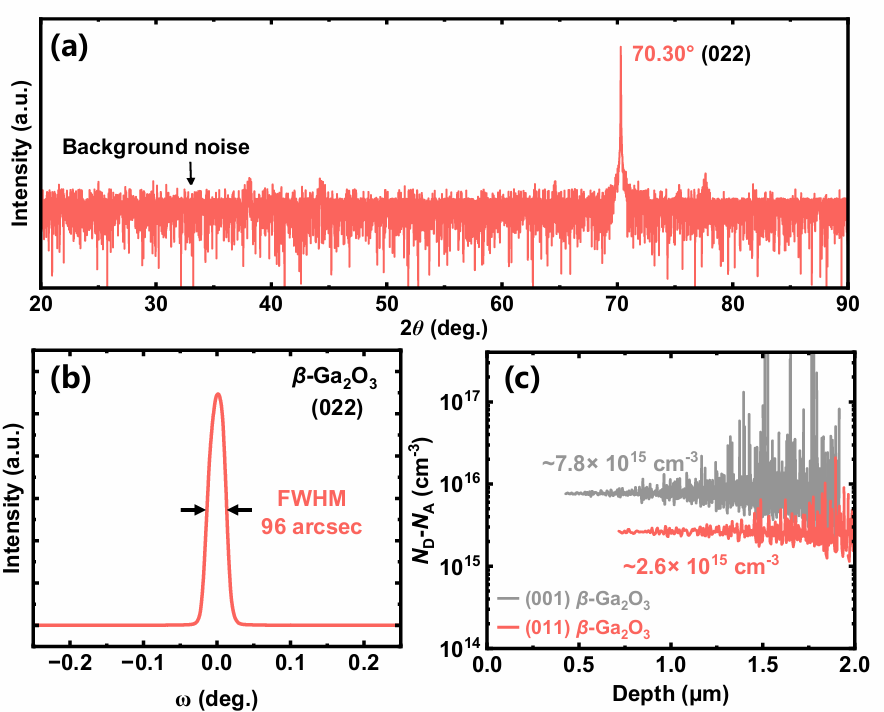
Fig. 2 (a) HRXRD 2theta-omega scans and (b) the rocking curve of the (011) β-Ga₂O₃ epi-layer. (c) The net carrier concentrations extracted from C-V measurements versus depth of the (011) and (001) epi-layers.
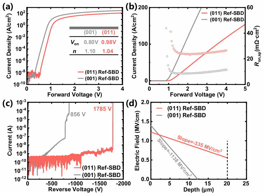
Fig. 3 The forward I-V characteristics of (011) and (001) Ref-SBD (a) with semi-logarithmic scale and (b) linear scale. (c) The reverse I-V characteristics of (011) and (001) Ref-SBD. (d) Theoretical electric field within the (011) and (001) epi-layer.
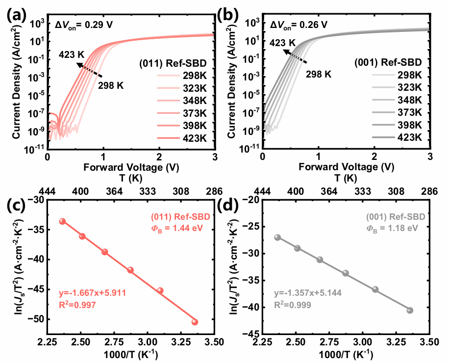
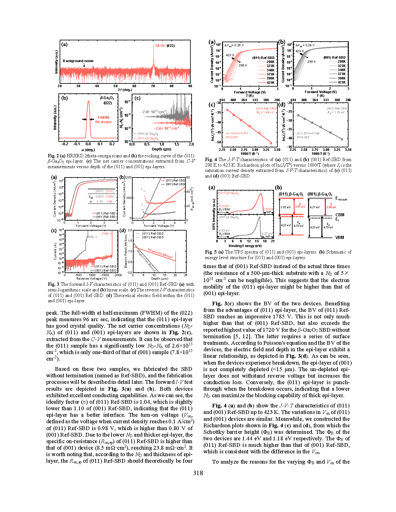
Fig. 4 The J-V-T characteristics of (a) (011) and (b) (001) Ref-SBD from 298 K to 423 K. Richardson plots of ln(Js/T2) versus 1000/T (where Js is the saturation current density extracted from J-V-T characteristics) of (c) (011) and (d) (001) Ref-SBD.
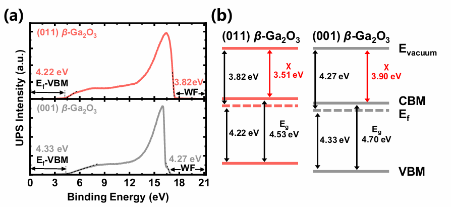
Fig. 5 (a) The UPS spectra of (011) and (001) epi-layers. (b) Schematic of energy level structure for (011) and (001) epi-layers.
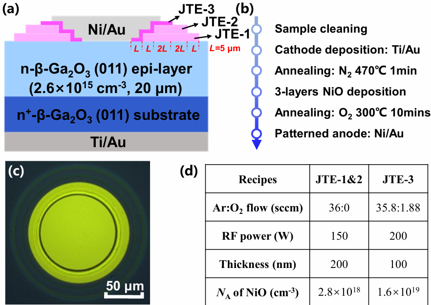
Fig. 6 (a) Schematic cross-section and (b) fabrication details of (011) 3 layers JTE-SBD. (c) The optical microscope image of the JTE-SBD. (d) The sputtering conditions and parameters of NiO in this work. The NA of NiO is extracted from the C-V results of fabricated HJD.
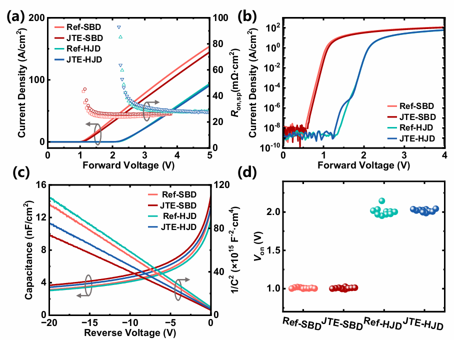
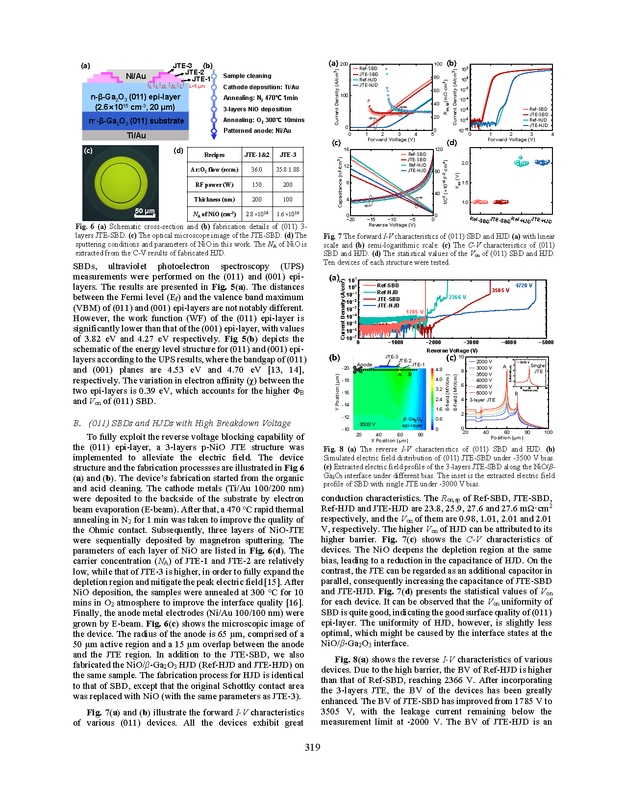
Fig. 7 The forward I-V characteristics of (011) SBD and HJD (a) with linear scale and (b) semi-logarithmic scale. (c) The C-V characteristics of (011) SBD and HJD. (d) The statistical values of the Von of (011) SBD and HJD. Ten devices of each structure were tested.
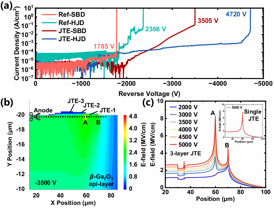
Fig. 8 (a) The reverse I-V characteristics of (011) SBD and HJD. (b) Simulated electric field distribution of (011) JTE-SBD under -3500 V bias. (c) Extracted electric field profile of the 3-layers JTE-SBD along the NiO/β Ga₂O₃ interface under different bias. The inset is the extracted electric field profile of SBD with single JTE under -3000 V bias.
DOI:
10.1109/ISPSD64561.2026.11553728
Instruction
Official Account

Cooperation
Top
