


Researchers from the Fuzhou University have published a dissertation titled " Conductance Modulation Mechanisms in Gallium Oxide-Based Neuromorphic Devices: From Device Physics to Intelligent Applications " in Advanced Materials Technologies.
Background
In the traditional von Neumann architecture, memory and processing units are physically separated, resulting in massive transmission power consumption and delay during data interaction, which cannot meet the low-power and real-time parallel computing requirements of the Internet of Things and edge artificial intelligence. Brain-inspired neuromorphic computing simulates the working modes of biological synapses and neurons to realize hardware-integrated storage and computation, serving as a critical solution to break the von Neumann bottleneck, with artificial synaptic devices as the core hardware unit.
Conventional synaptic materials including organics, quantum dots, perovskites, 2D materials and common oxides mostly exhibit photoresponse ranging from near-ultraviolet to near-infrared, failing to adapt to extreme working conditions such as deep-space exploration, high-temperature industry, nuclear radiation and solar-blind ultraviolet detection.
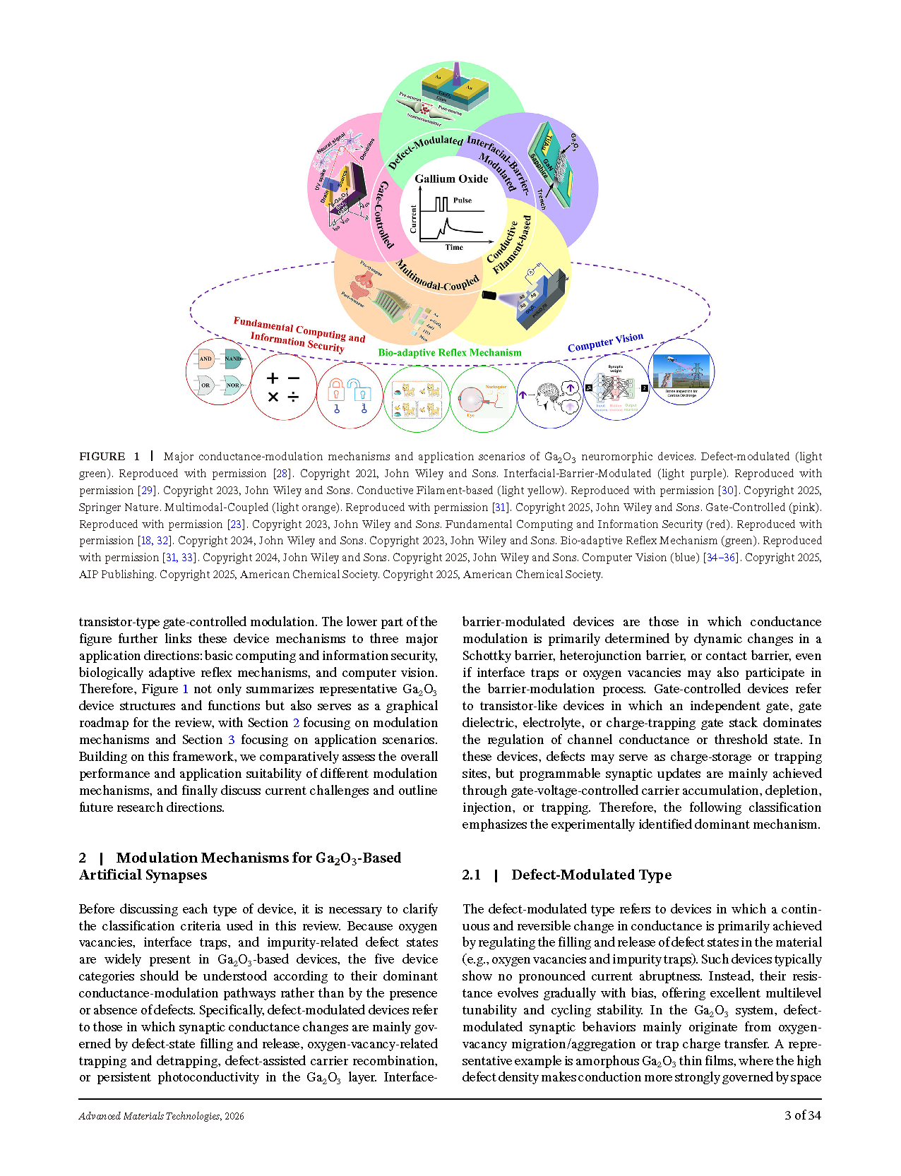
Ga₂O₃ is an ultrawide-bandgap semiconductor with a bandgap of 4.4–5.3 eV. It features an ultrahigh breakdown electric field, multiple polymorphs (α, β, ε, γ, δ), excellent thermal stability and precise controllable doping. It has intrinsic solar-blind UV response without visible light crosstalk. The low formation energy of oxygen vacancies easily induces persistent photoconductivity (PPC), which can mimic short-term memory (STM) and long-term memory (LTM). Doping modification, phase engineering and heterostructure integration can extend its synaptic response to visible light and X-rays. Meanwhile, Ga₂O₃ supports five conductance modulation pathways: defect modulation, interfacial barrier modulation, conductive filament modulation, multimodal coupling and gate voltage modulation, compatible with synaptic behaviors co-triggered by optical, electrical and mechanical stimuli.
Existing research on various Ga₂O₃-based synaptic devices is scattered. No review systematically sorts out device physics, structures, synaptic functions and full-scenario applications classified by dominant conductance modulation mechanisms. This paper fills this gap and comprehensively summarizes modulation mechanisms, device architectures, cutting-edge applications and remaining challenges.
Abstract
This review systematically surveys the recent progress in gallium oxide-based neuromorphic devices. As an ultrawidebandgap semiconductor, Ga₂O₃ offers controllable doping, an exceptionally high breakdown electric field, multiple polymorphs, and excellent thermal stability. These intrinsic properties make Ga₂O₃ particularly suitable for neuromorphic devices operating under high-temperature, strong-radiation, and solar-blind deep-ultraviolet (DUV) conditions. Beyond environmental stability, Ga₂O₃ can also support diverse conductance-modulation mechanisms, including defect-mediated carrier trapping, interface-barrier engineering, conductive-filament evolution, multimodal coupling, and gate-controlled channel modulation, thereby providing a versatile material platform for programmable synaptic devices driven by optical, electrical, or coupled external stimuli. Starting from the conductance-modulation mechanisms underlying synaptic functions, we classify Ga₂O₃ neuromorphic devices and systematically summarize their physical mechanisms, structural designs, and conductance-tuning schemes, highlighting the potential of Ga₂O₃ for neuromorphic computing, low-power operation, and spectrally selective sensing, as well as its broad prospects in fundamental computing and information security, bio-adaptive reflex mechanisms, and computer vision. Finally, we summarize the progress and remaining challenges of Ga₂O₃ neuromorphic devices, and outline future research directions including materials doping, heterostructure integration, multimodal fusion, high-density arrays, and energy-efficiency optimization to fully exploit Ga₂O₃ for brain-inspired computing and intelligent perception.
Highlights
For the first time, all existing Ga₂O₃-based neuromorphic devices are categorized into five types dominated by conductance modulation mechanisms: defect-modulated, interfacial-barrier-modulated, conductive-filament-based, multimodal-coupled and gate-controlled devices. The carrier transport physics, typical architectures and synaptic plasticity schemes of each category are systematically summarized to eliminate messy classification and mixed mechanisms in previous reviews.
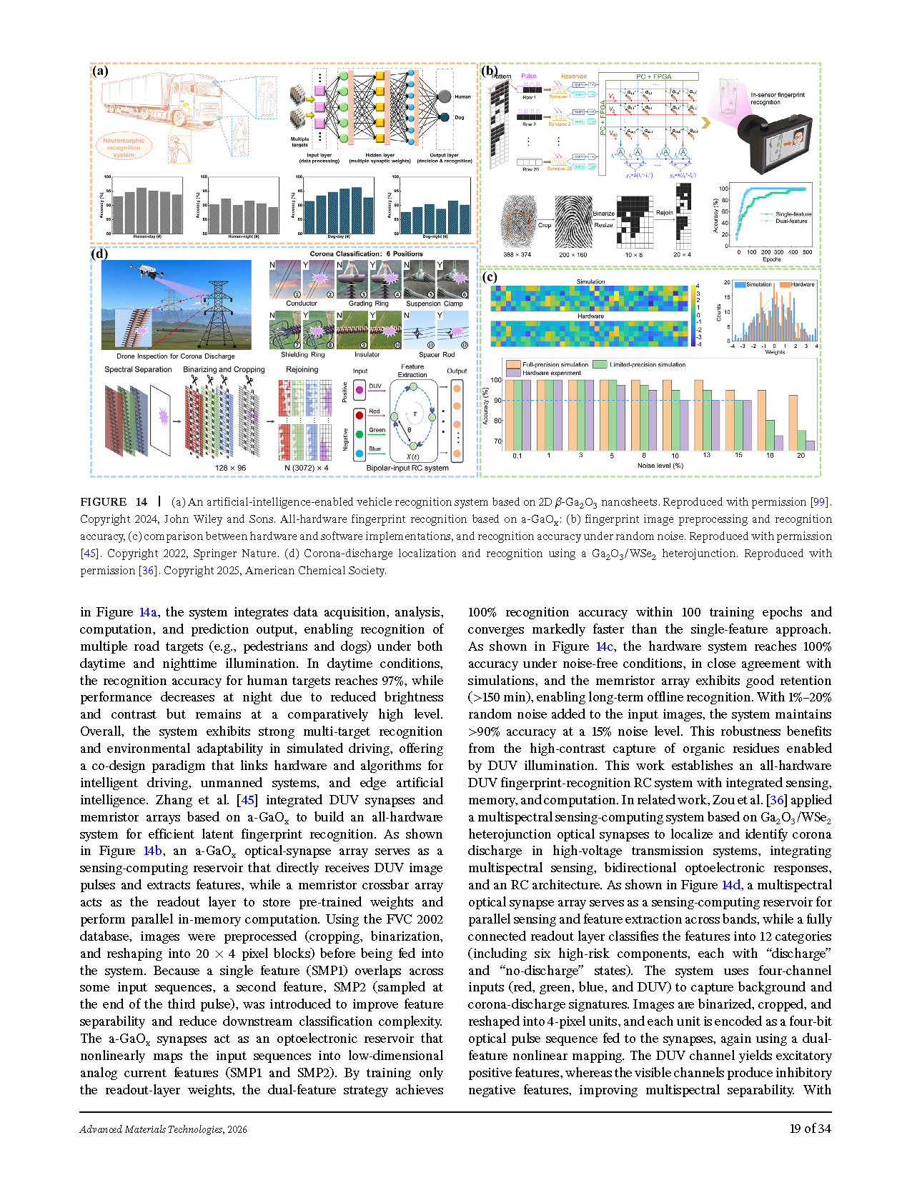
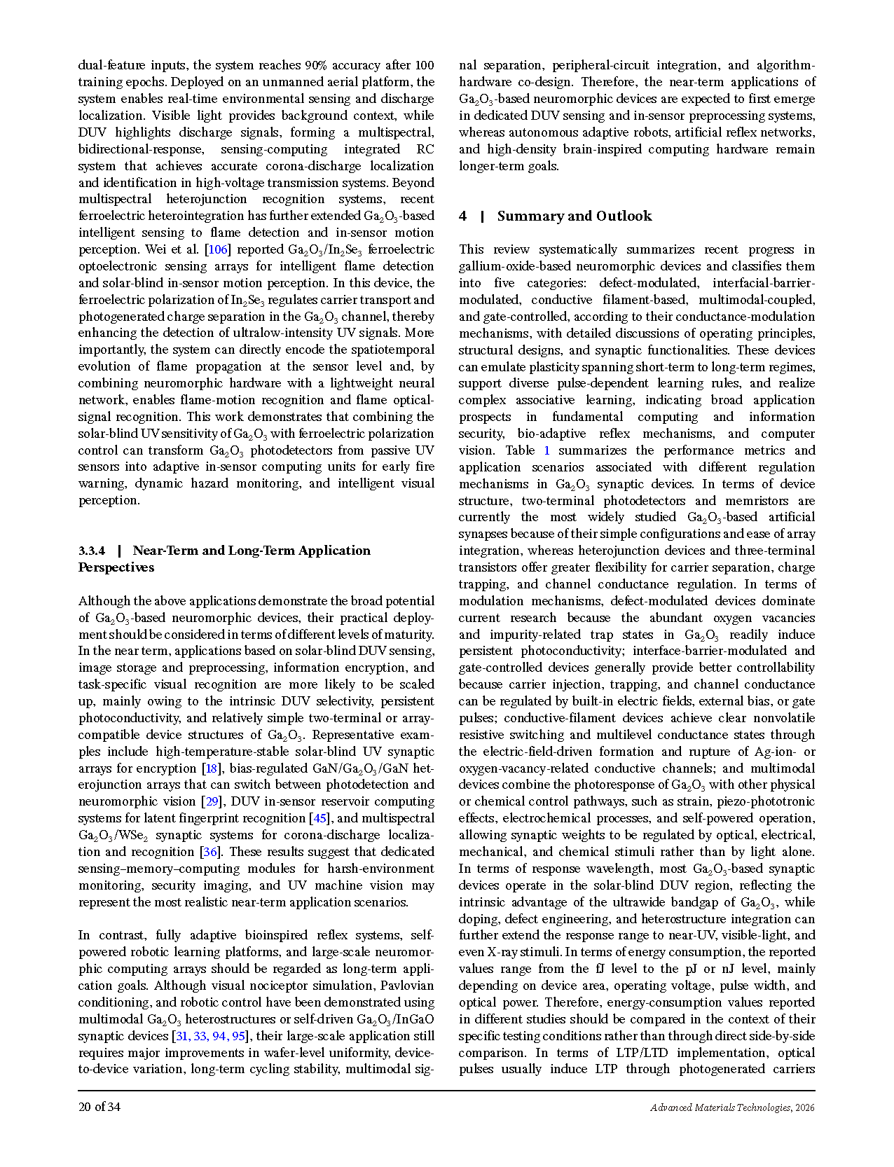
All application scenarios of Ga₂O₃ synaptic devices are fully covered and divided into three major fields: fundamental computing & information security, bio-adaptive reflex emulation and computer vision, including logic operation, equation solving, data encryption, Pavlovian conditioning, nociceptor simulation, image memory & classification, medical CT diagnosis, high-voltage corona detection and autonomous robot learning.
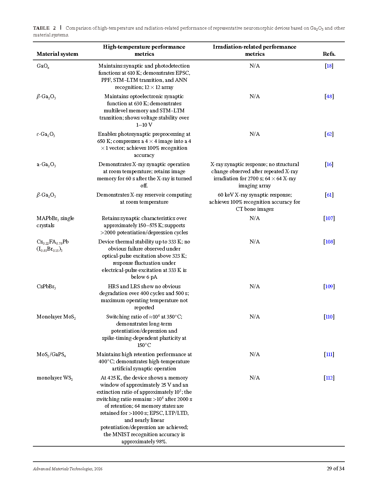
A horizontal performance comparison among Ga₂O₃, perovskite and 2D material neuromorphic devices under high temperature and irradiation is conducted, verifying the unique comprehensive merits of Ga₂O₃ for extreme-environment sensing-computing integration: combined high thermal tolerance, radiation hardness, intrinsic solar-blind selectivity and X-ray synaptic response.
Critical industrial bottlenecks of Ga₂O₃ are comprehensively analyzed, including lack of reliable p-type doping, poor wafer-scale device uniformity, trade-off between switching speed and retention, and high power consumption. Practical short-to-medium strategies are proposed: heterointegration with p-type oxides, ferroelectric/floating-gate/electrolyte substitution for bulk p-type Ga₂O₃, low-temperature compatible fabrication, precise defect energy level engineering and self-powered system optimization.
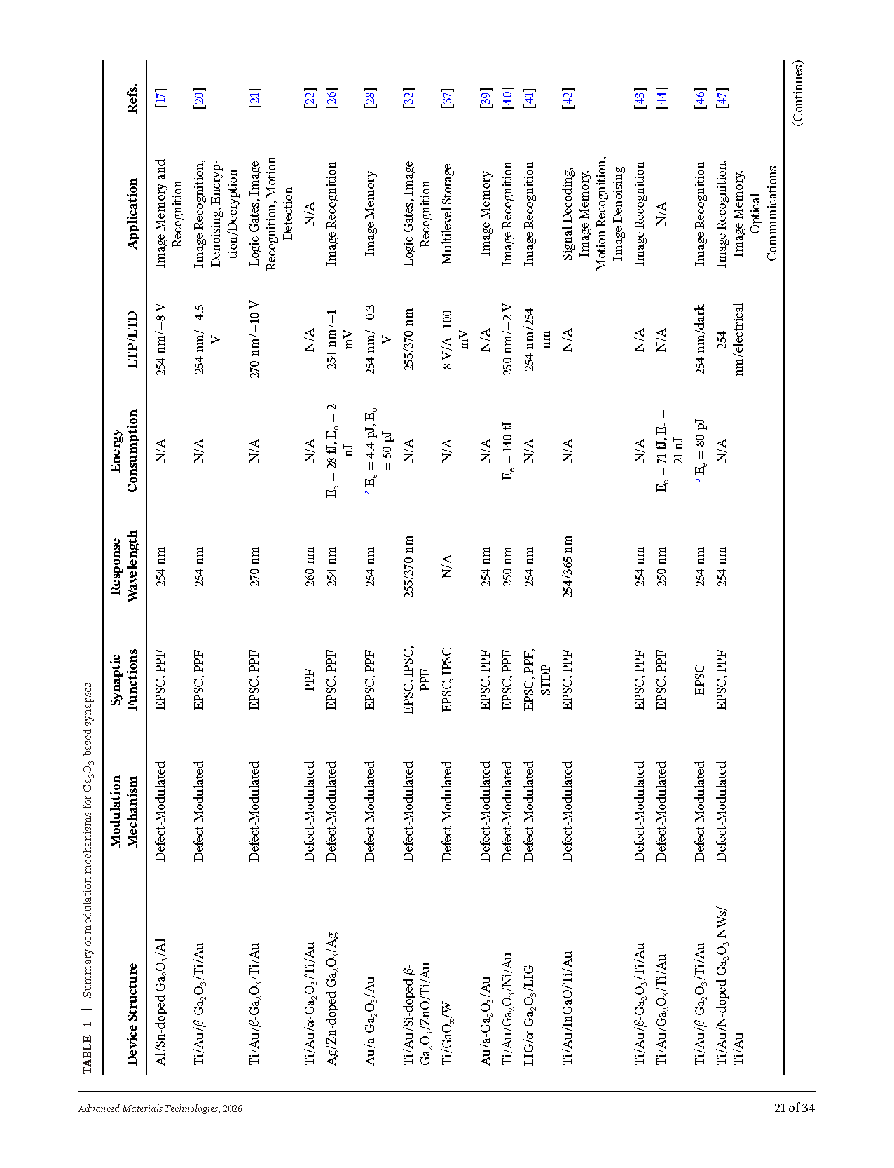
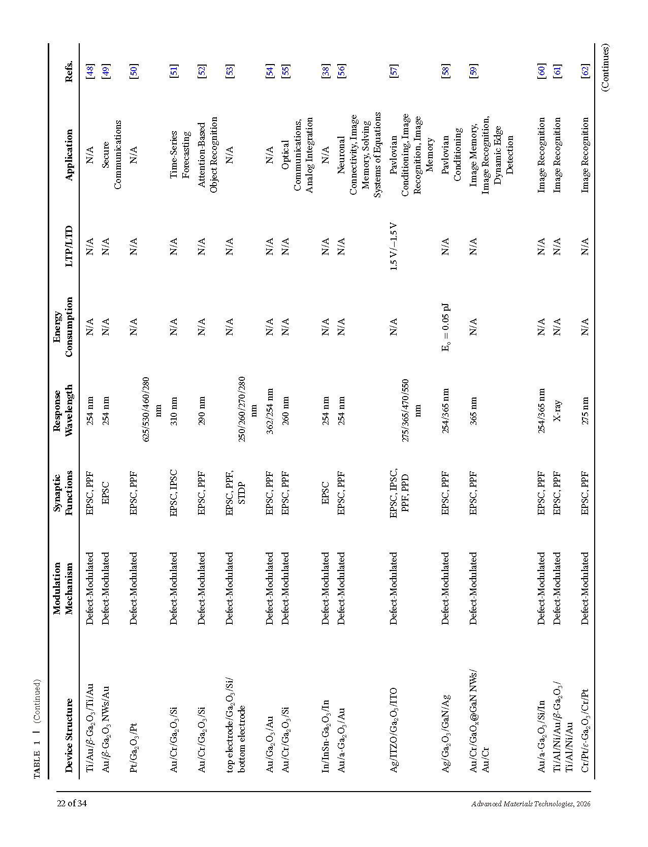
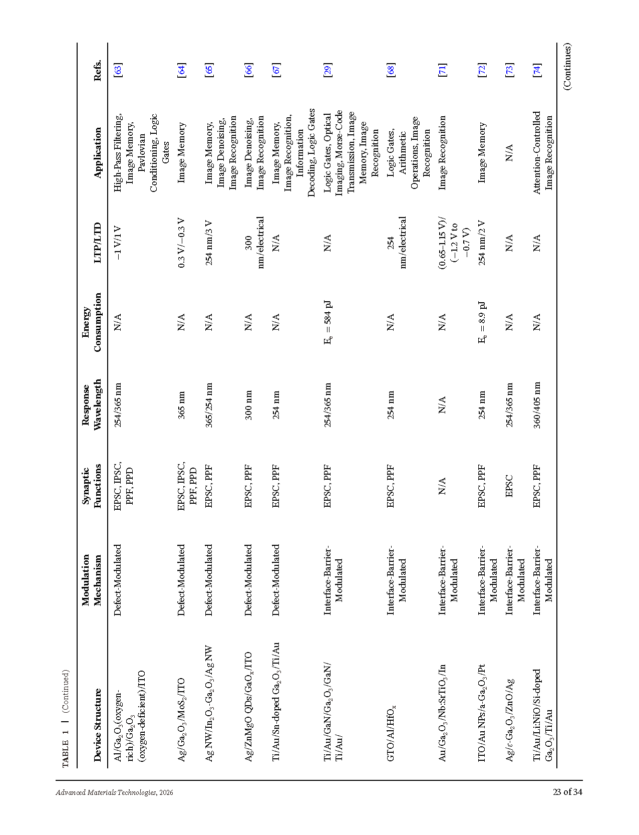
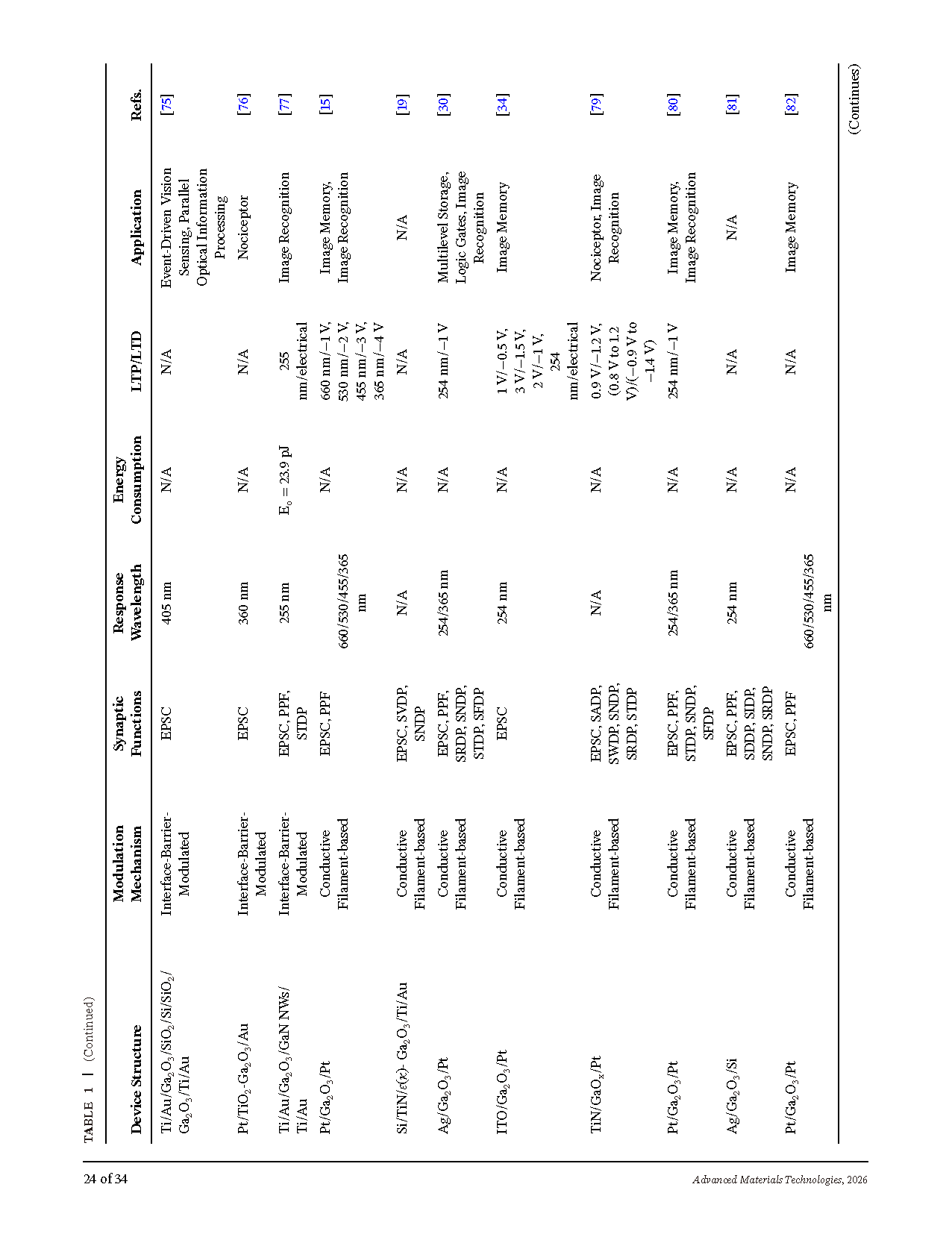
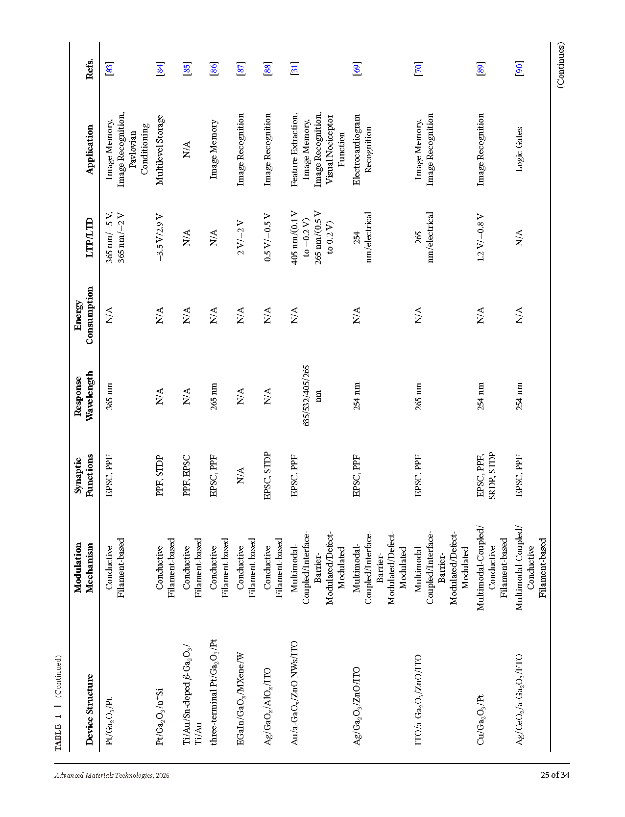
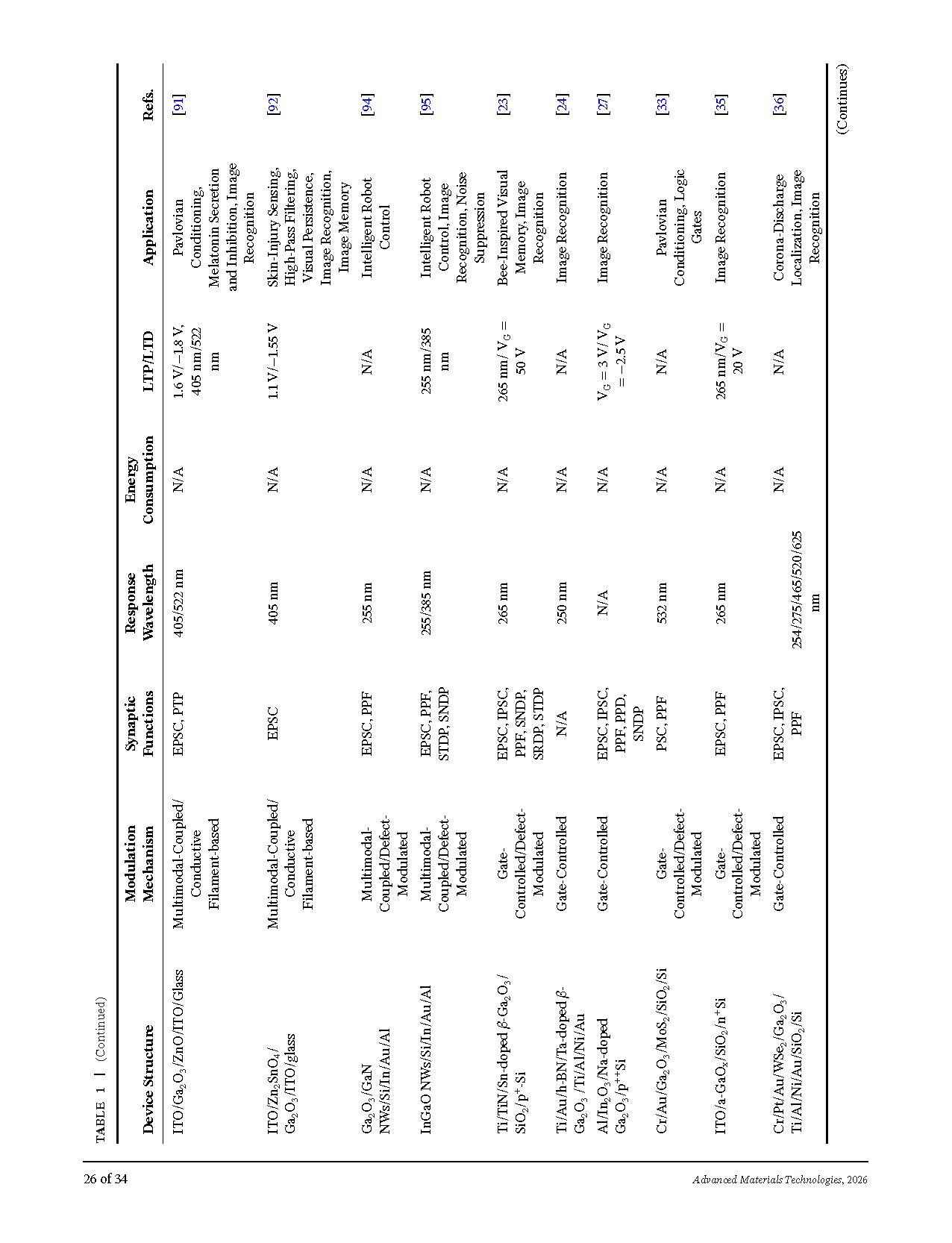
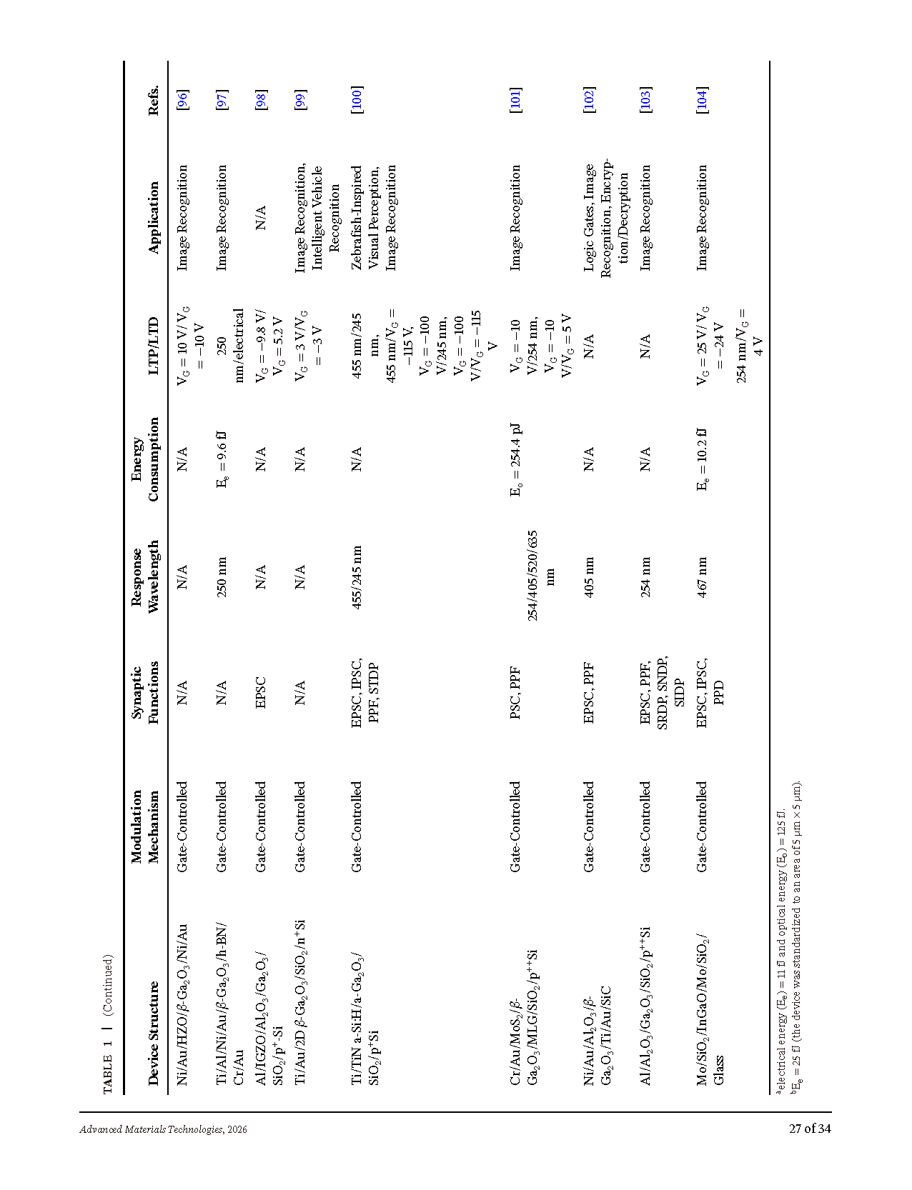
Comprehensive quantitative comparison tables are established to summarize device structures, modulation physics, synaptic functions, response spectra, energy consumption, LTP/LTD strategies and references for five device categories, offering standardized guidance for subsequent device design and mechanism exploration.
Conclusion
Owing to its distinctive material characteristics and versatile device architectures, gallium oxide demonstrates substantial research value in neuromorphic electronics. With an ultrawide bandgap and a robust crystal structure, Ga₂O₃ synaptic devices can operate reliably under extreme conditions where conventional materials fail, such as high temperatures and intense radiation. A growing body of work shows that Ga₂O₃ artificial synapses not only enable high-speed, low-power resistive switching memory and analog computing, but also exhibit spectrally selective sensing, thereby integrating sensing and computing within a single device. This attribute is particularly valuable for edge computing nodes of the Internet of Things and next-generation intelligent vision systems, because sensors can directly output preprocessed, task-relevant information, reducing both backend processing and data transmission. Notably, for aerospace and nuclear detection applications, the radiation hardness and high-temperature tolerance of Ga₂O₃ make it a strong candidate for brain-inspired autonomous learning systems in harsh environments.
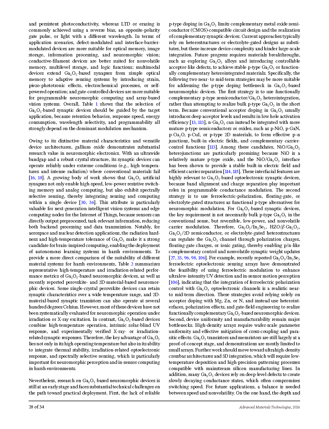
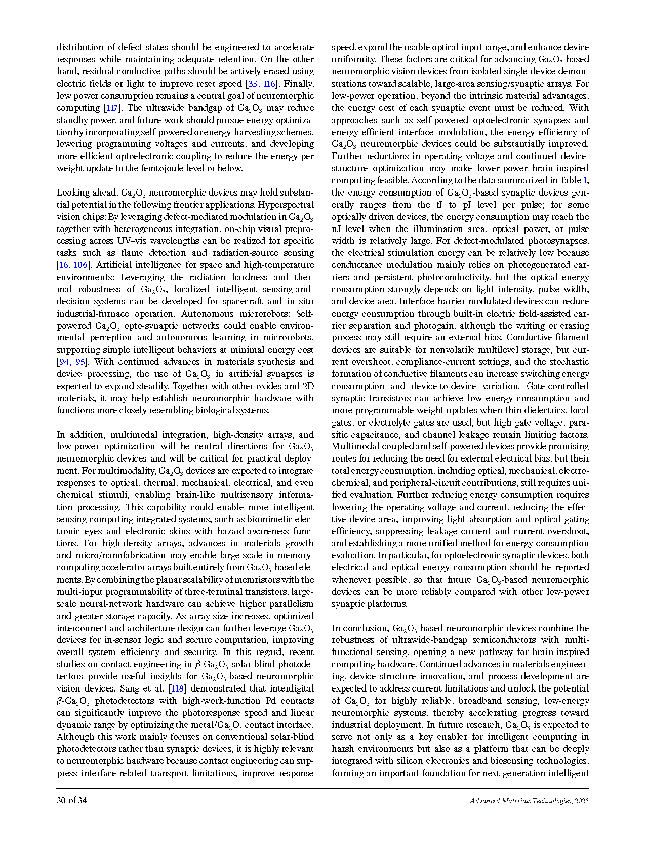
Nevertheless, research on Ga₂O₃-based neuromorphic devices is still at an early stage and faces substantial technical challenges on the path toward practical deployment. First, the lack of reliable p-type doping limits complementary metal oxide semiconductor (CMOS)-compatible circuit design and the realization of complementary synaptic devices. Current substitutes including heterostructures and electrolyte-gated devices increase device complexity and hinder large-scale integration. Second, wafer-level device uniformity, array crosstalk and parasitic effects remain difficult to suppress, and breakthroughs are required for ultrahigh-density crossbar arrays and three-dimensional integration. Meanwhile, many devices rely on deep-level defects to generate slowly decaying conductance states, which sacrifices switching speed; a balance between response speed and nonvolatile retention must be achieved in future development. Finally, low power consumption remains a central goal of neuromorphic computing. The ultrawide bandgap of Ga₂O₃ reduces standby power, and further progress should combine self-powered and energy-harvesting schemes, lower operating voltages and currents, and reduce the energy per weight update to the femtojoule level.
Looking ahead, Ga₂O₃ neuromorphic devices may hold substantial potential in three frontier directions: hyperspectral vision chips, artificial intelligence for space and high-temperature environments, and autonomous microrobots. With continuous advances in materials doping, heterogeneous integration, multimodal fusion, high-density arrays and energy-efficiency optimization, Ga₂O₃ is expected to work together with other oxides and two-dimensional materials to establish brain-like hardware systems. As fabrication processes evolve, multimodal sensing integration, large-scale in-memory computing arrays and ultra-low-power synaptic hardware will be gradually deployed, opening new research tracks including intelligent perception for harsh environments, silicon-circuit compatible integration and biosensor fusion. With coordinated efforts from academia and industry, Ga₂O₃ neuromorphic electronics may significantly accelerate the industrialization of artificial brain hardware.
Project Support
This work was supported by the National Science and Technology Major Project (No. 2025ZD0616200), the National Key Research and Development Program of China (No. 2022YFB3606603), and the Fujian Science & Technology Innovation Laboratory for Optoelectronic Information of China (Nos. 2020ZZ111, 2020ZZ113, and 2021ZZ130).
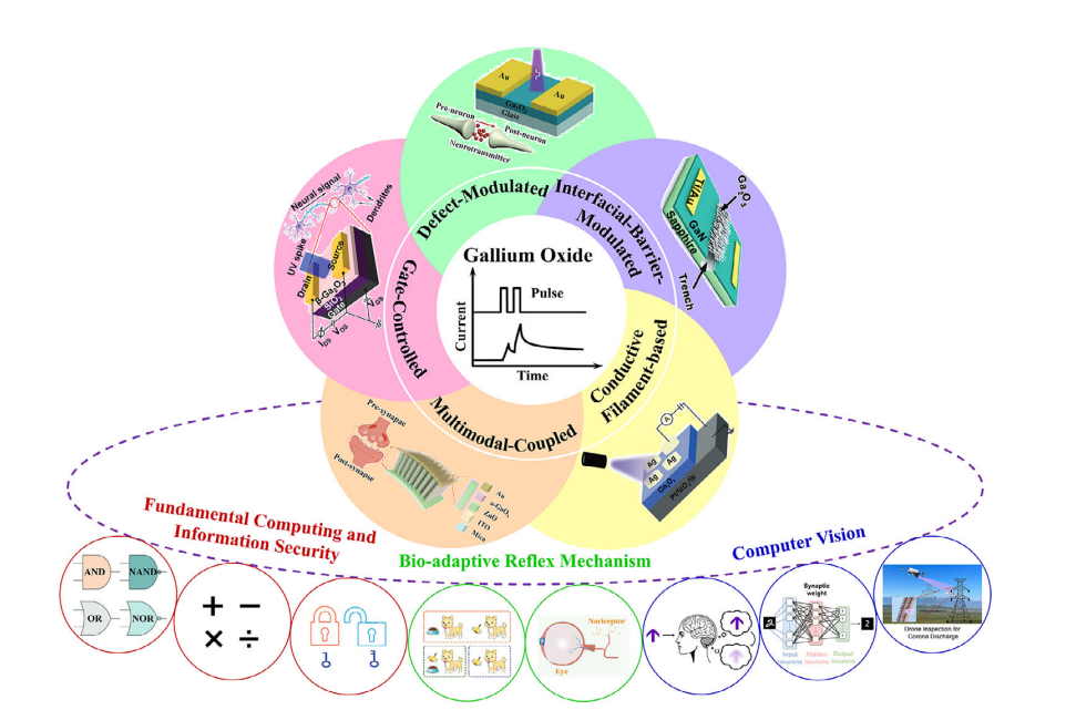
Figure 1 Major conductance-modulation mechanisms and application scenarios of Ga₂O₃ neuromorphic devices.
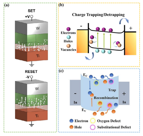
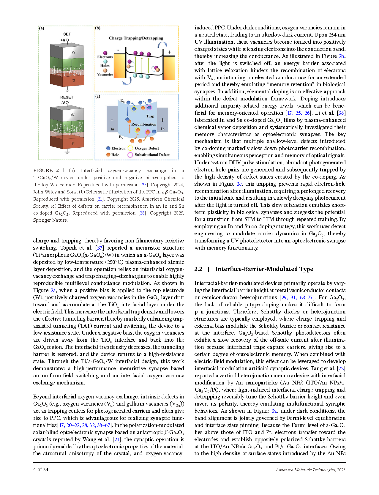
Figure 2 (a) Interfacial oxygen-vacancy exchange in a Ti/GaOₓ/W device under positive and negative biases applied to the top W electrode. (b) Schematic illustration of the PPC in a β-Ga₂O₃. (c) Effect of defects on carrier recombination in an In and Sn co-doped Ga₂O₃.
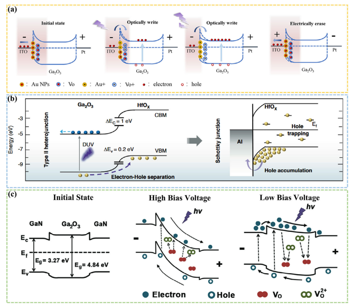
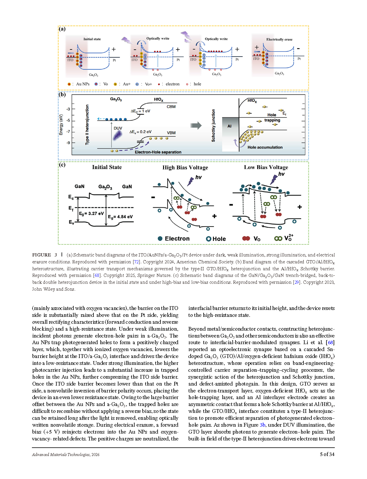
Figure 3 (a) Schematic band diagrams of the ITO/AuNPs/a-Ga₂O₃/Pt device under dark, weak illumination, strong illumination, and electrical erasure. (b) Band diagram of the cascaded GTO/Al/HfOₓ heterostructure, illustrating carrier transport mechanisms governed by the type-II heterojunction and the Al/HfOₓ Schottky barrier. (c) Schematic band diagrams of the GaN/Ga₂O₃/GaN trench-bridged, back-to-back double heterojunction device in the initial state and under high-bias and low-bias conditions.
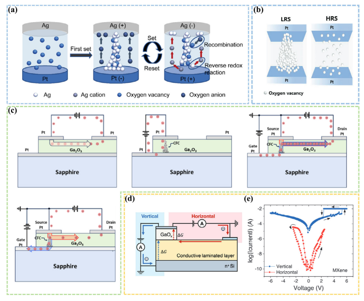
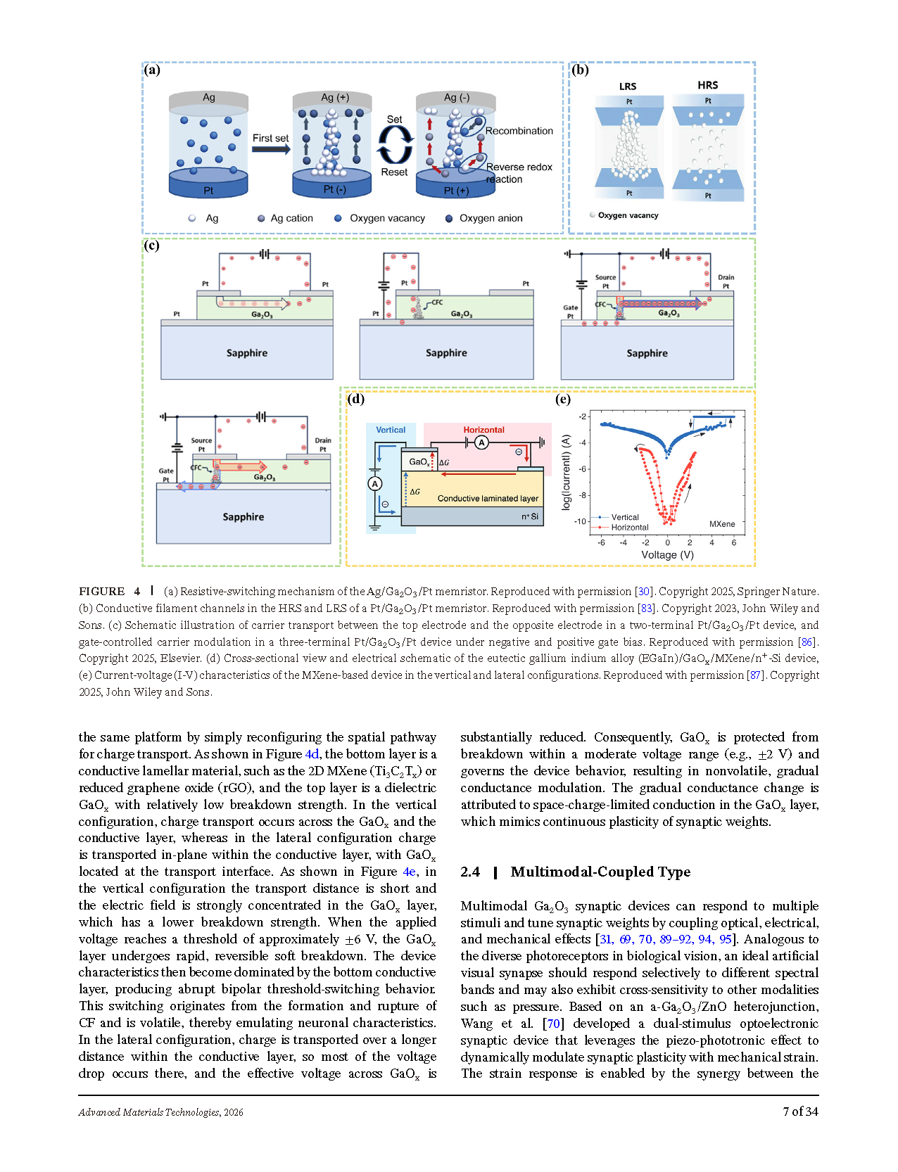
Figure 4 (a) Resistive-switching mechanism of the Ag/Ga₂O₃/Pt memristor. (b) LRS and HRS conductive filament channel diagram of Pt/Ga₂O₃ memristor. (c) Schematic illustration of carrier transport between the top and bottom electrode in two-terminal Pt/Ga₂O₃/Pt device and gate-controlled carrier modulation in three-terminal Pt/Ga₂O₃/Pt device under negative and positive gate bias. (d) Cross-sectional view and electrical schematic of eutectic gallium indium alloy/GaOₓ/MXene/n⁺-Si device. (e) I-V curves of vertical and lateral configurations of MXene-based bilayer memristive device.
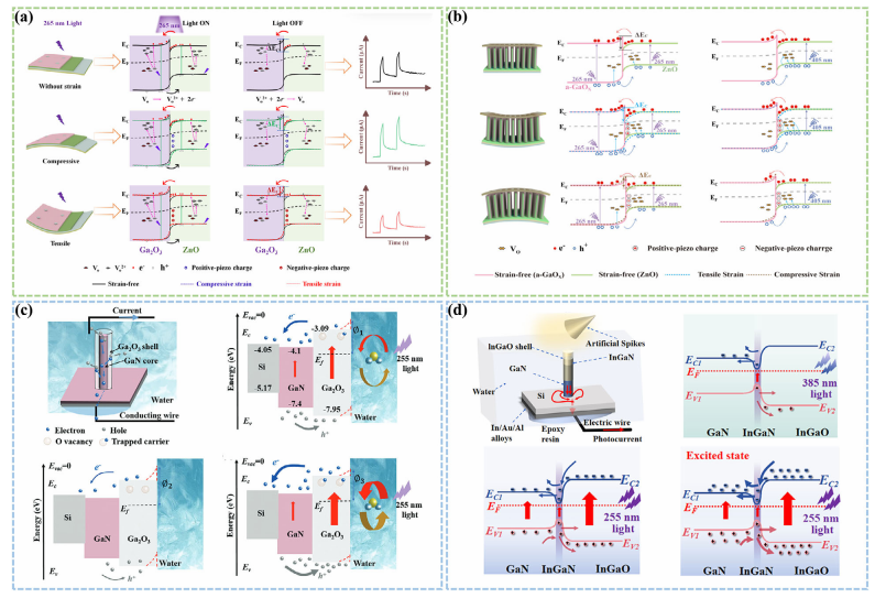
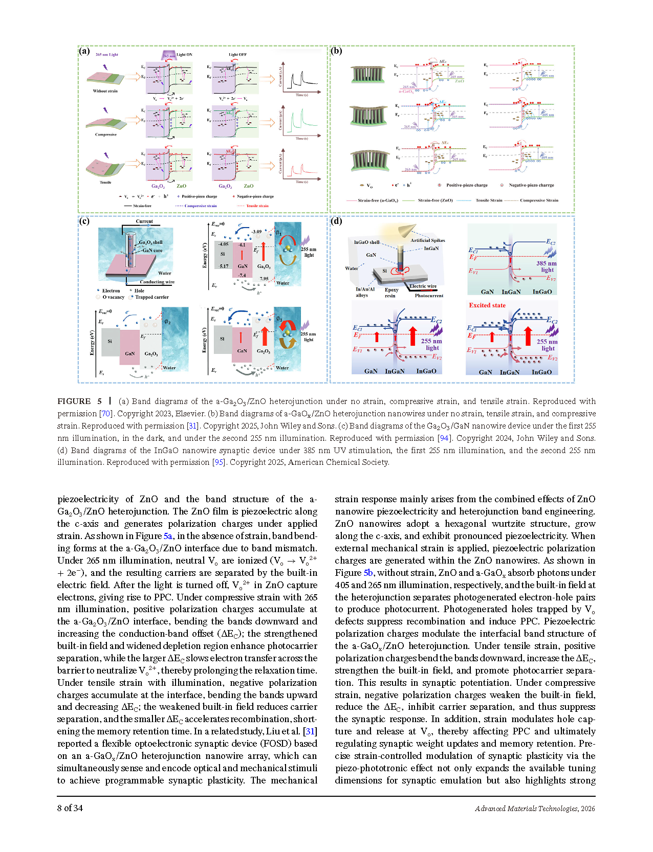
Figure 5 (a) Band diagrams of a-Ga₂O₃/ZnO heterojunction under no strain, compressive strain, and tensile strain. (b) Band diagrams of a-GaOₓ/ZnO heterojunction nanowires under no strain, tensile strain, and compressive strain. (c) Band diagrams of Ga₂O₃/GaN nanowire device under first 255 nm illumination, dark state, and second 255 nm illumination. (d) Band diagrams of InGaO nanowire synaptic device under 385 nm UV, first 255 nm UV, second 255 nm UV irradiation
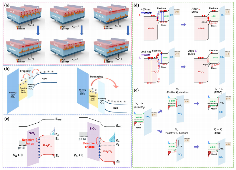
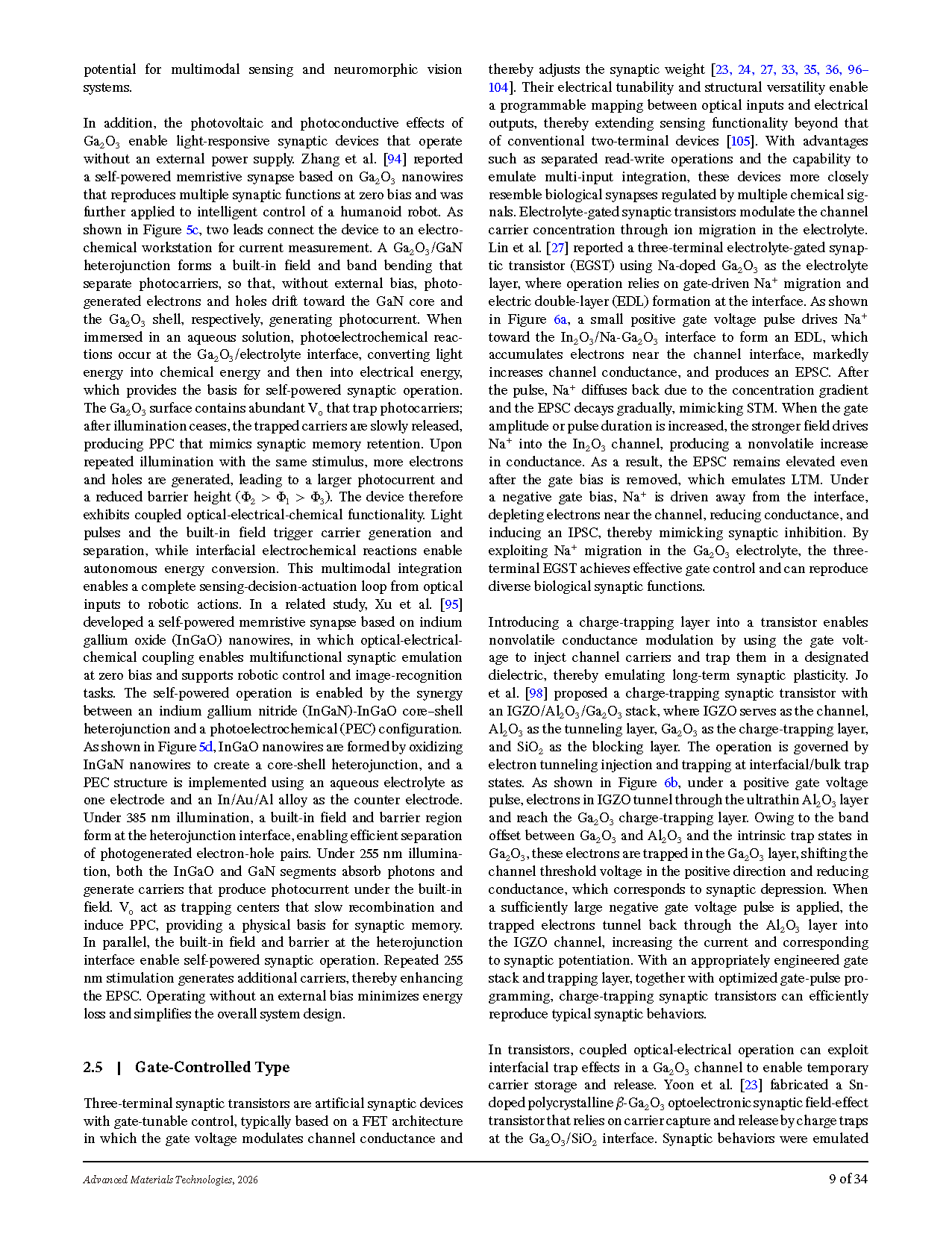
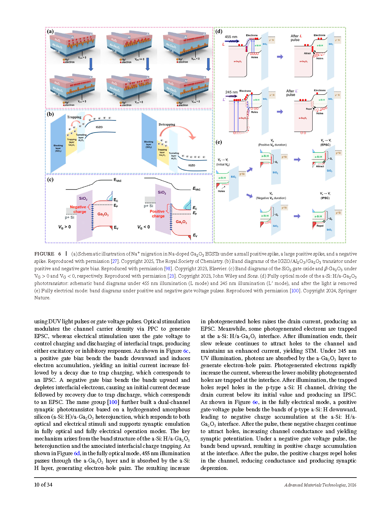
Figure 6 (a) Schematic illustration of Na⁺ migration in Na-doped Ga₂O₃ electrolyte-gated synaptic transistor under small positive spike, large positive spike, negative spike. (b) Band diagrams of IGZO/Al₂O₃/Ga₂O₃ transistor under positive and negative gate bias. (c) Band diagrams of SiO₂/β-Ga₂O₃ under VG>0 and VG<0. (d) Fully optical operation band diagram of a-Si:H/a-Ga₂O₃ phototransistor under 455 nm and 245 nm illumination; (e) Fully electrical band diagram under positive and negative gate voltage pulses.
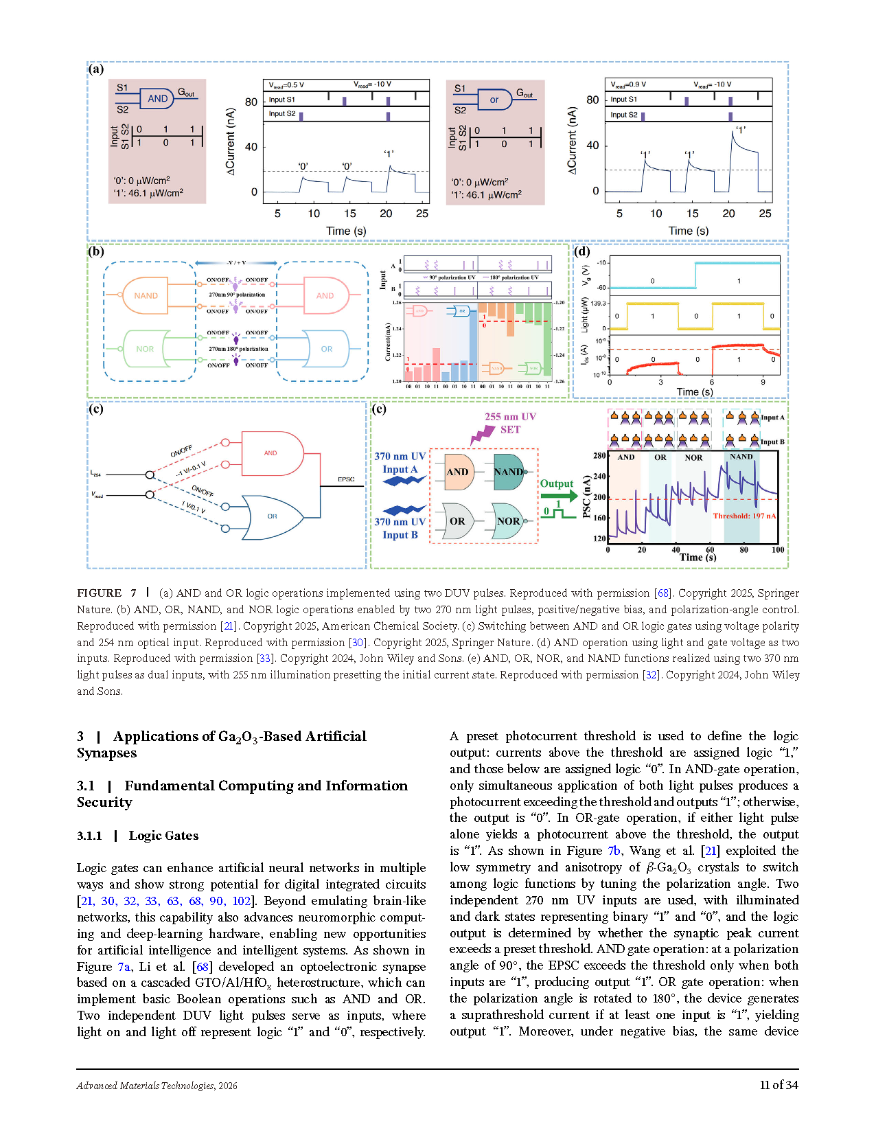
Figure 7 (a) AND and OR logic operations realized by two independent DUV pulse inputs. (b) AND, OR, NAND, NOR logic functions modulated by polarization angle and bias voltage with dual 270 nm UV inputs. (c) AND/OR logic switching controlled by voltage polarity and 254 nm optical signal. (d) AND gate implemented by light and gate voltage dual inputs. (e) AND, OR, NOR, NAND logic realized by two 370 nm UV pulses with 255 nm preset illumination.
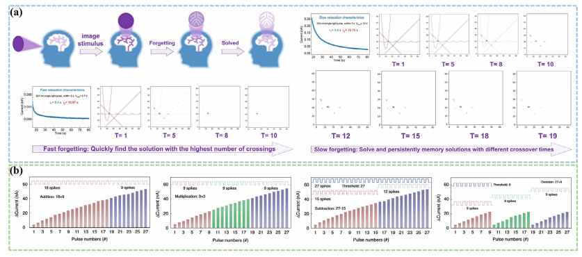
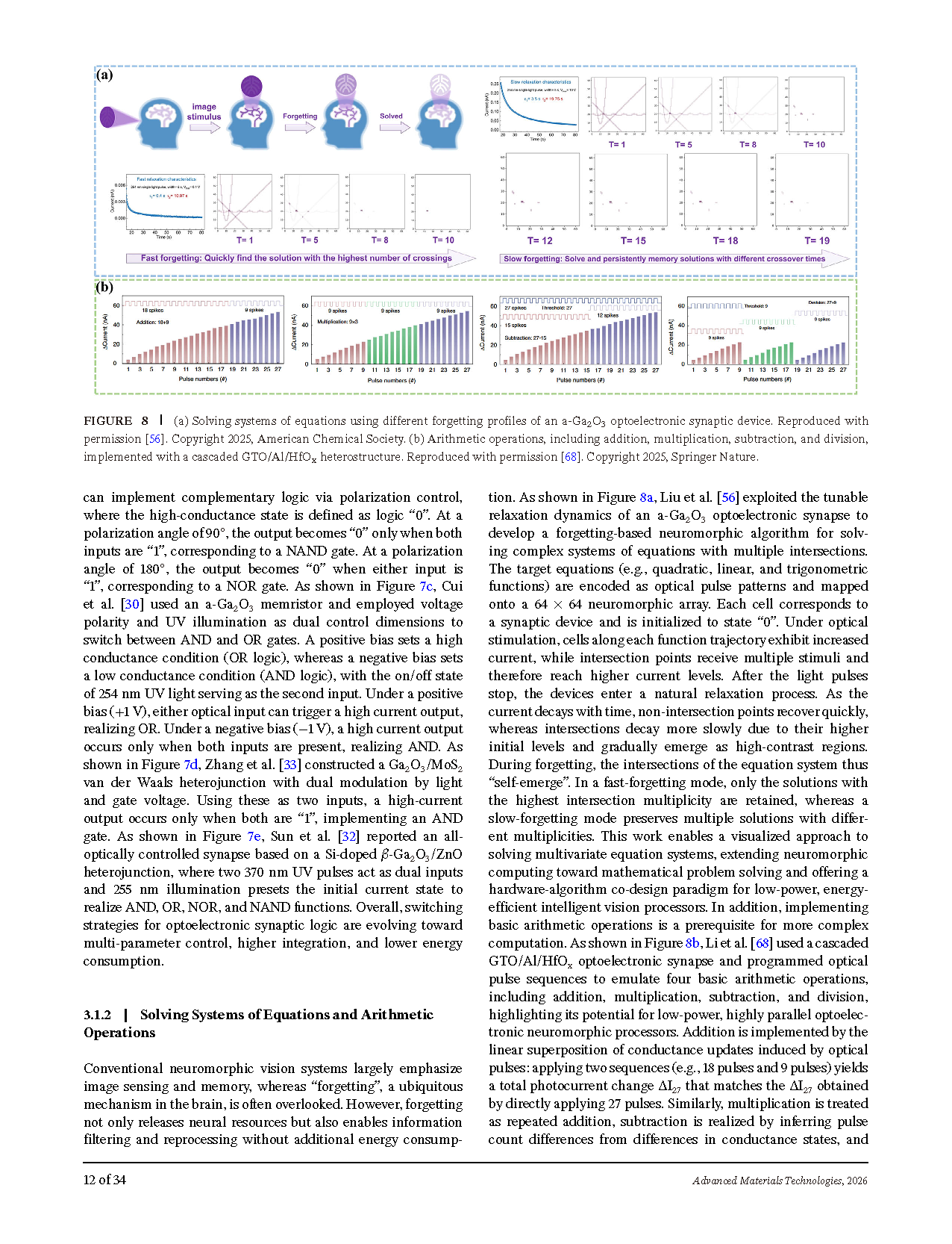
Figure 8 (a) Solving systems of equations utilizing tunable forgetting dynamics of a-Ga₂O₃ optoelectronic synaptic array. (b) Addition, subtraction, multiplication, division arithmetic operations based on cascaded GTO/Al/HfOₓ heterostructure synapse.
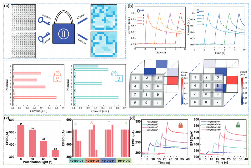
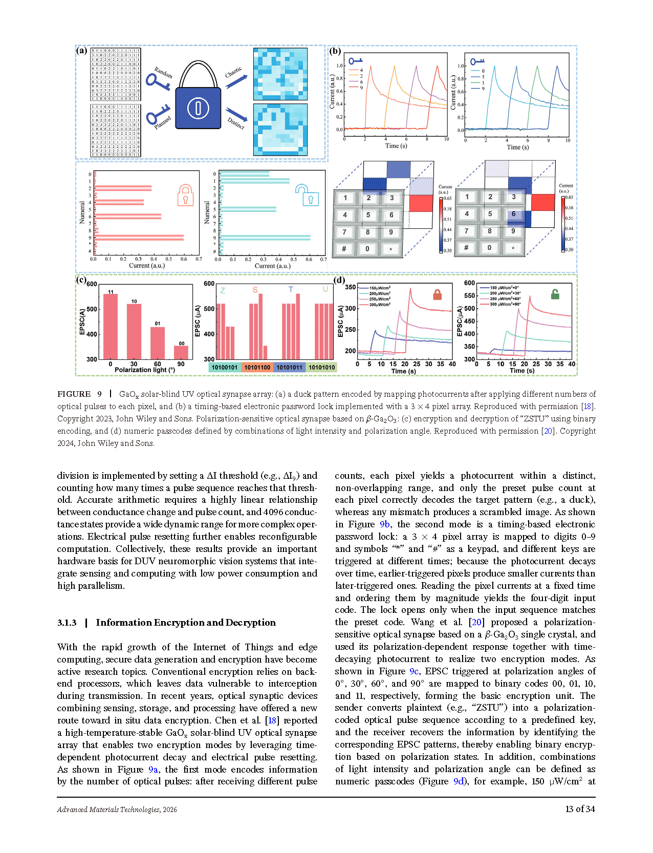
Figure 9 (a) Encoded duck pattern by varying optical pulse numbers on each pixel of GaOₓ solar-blind UV synaptic array; (b) Timing-based password lock based on 3 × 4 pixel synaptic array. (c) Binary encryption and decryption of text "ZSTU" via polarization-dependent EPSC of β-Ga₂O₃ single crystal synapse; (d) Numeric passcode constructed by combined light intensity and polarization angle.
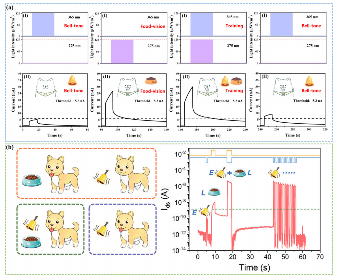
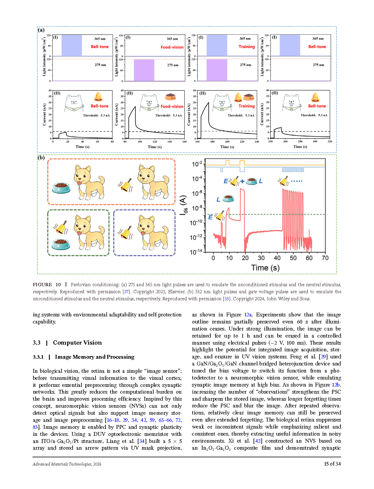
Figure 10 (a) Fully optical Pavlovian conditioning using 275 nm unconditioned stimulus and 365 nm neutral stimulus light pulses; (b) Optoelectronic hybrid Pavlovian conditioning with 532 nm light as unconditioned stimulus and gate voltage pulse as neutral stimulus.
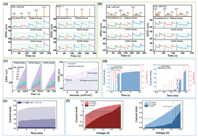
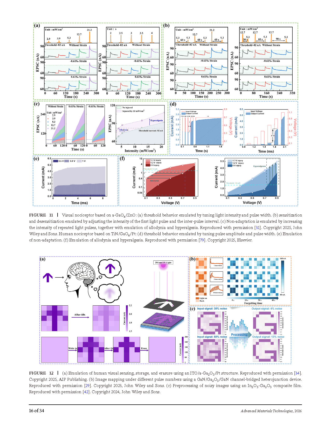
Figure 11 (a) Threshold nociceptor behavior modulated by light intensity and pulse width on a-GaOₓ/ZnO heterojunction device; (b) Sensitization and desensitization behaviors regulated by pre-stimulus intensity and inter-pulse interval; (c) Non-adaptation, allodynia and hyperalgesia emulated by increasing light intensity and post-injury stimulation; (d) Threshold characteristic of TiN/GaOₓ/Pt memristor controlled by electrical pulse amplitude and width; (e) Non-adaptation response under consecutive electrical pulses; (f) Allodynia and hyperalgesia after high-amplitude injury pulse.
DOI :
10.1002/admt.71146
Instruction
Official Account

Cooperation
Top
