


Researchers from the Inner Mongolia University and Nanjing University of Posts and Telecommunications have published a dissertation titled "Enhanced Light–Matter Interaction and Efficient Energy Transfer in Ga2O3 Photodetectors Based on van der Waals Heterogeneous Structures" in ACS Photonics.
Background
Gallium oxide (Ga₂O₃), an ultra-wide bandgap semiconductor with an optical bandgap of ~4.8 eV, only responds to solar-blind deep ultraviolet (DUV) light ranging from 200 to 280 nm. There is no natural UVC radiation on the Earth’s surface due to ozone shielding, so Ga₂O₃ photodetectors feature low background noise and superior detection sensitivity, making them a leading candidate for deep ultraviolet optoelectronic sensing. Single-component Ga₂O₃ devices suffer from inherent limitations: there is an intrinsic trade-off between light absorbance and light–matter interaction; standalone Ga₂O₃ thin films cannot simultaneously realize strong UV absorption and efficient photocarrier separation. Conventional device architectures including MSM, Schottky diodes and homojunctions are limited by lattice mismatch, interfacial dangling bonds and oxygen vacancy defects. High-density interface states trap photogenerated carriers, leading to an unavoidable compromise between responsivity and response speed, high dark current and poor long-term stability.
Traditional chemically bonded heterojunctions suffer severe lattice mismatch at hetero-interfaces, which generates dense defect energy levels acting as carrier traps and drastically suppresses energy transfer efficiency. In contrast, van der Waals (vdW) heterostructures are stacked via weak intermolecular forces, free from lattice matching constraints and interfacial chemical bonding. Their dark current can be modulated by external electric fields, effectively eliminating carrier traps and fundamentally mitigating the performance trade-off between high responsivity and fast response. At present, diverse vdW heterostructures can be fabricated by combining Ga₂O₃ with two-dimensional materials, organic semiconductors and p-type doped Ga₂O₃. However, a systematic analysis of the underlying mechanisms governing light–matter coupling and interfacial energy transfer across various vdW hetero-interfaces remains absent, and numerous challenges in material engineering, interface control and device fabrication hinder their practical large-scale deployment. This review comprehensively summarizes advances in Ga₂O₃-based vdW heterojunction DUV photodetectors and analyzes intrinsic interfacial mechanisms to provide theoretical guidelines for high-performance solar-blind photodetector design.
Abstract
New generation wide bandgap semiconductor gallium oxide (Ga₂O₃), with a decent optical bandgap and absorbance cutoff wavelength, has been a desired material for constructing deep-ultraviolet photodetectors, highlighting advantages of low noise and high sensitivity. Considering two key matters, “light−matter interaction” and “light absorbance”, influencing the photodetection performance, additional materials are required to fabricate heterostructures with Ga₂O₃ to overcome the intrinsic limitations of a single material. A compensatory material should be chosen to develop heterointerfaces with Ga₂O₃ to collect excitons, concerning the photon excitation and carrier transport. This scheme would solve the conflict between strong light absorbance and weak light−matter interaction. The emerging van der Waals (vdW) system features free stacking, no surface-free bonding, and easy control of dark current by an external field, providing a new opportunity to study heterogeneous deep-ultraviolet optoelectronics, catering to the demand for developments in modern optics, materials science, physics, electronics, etc. Progress in materials preparation contributes to the convenience of fabrication of vdW heterojunctions to discover abundant novel optoelectronic properties in optoelectronic devices, which are desired in various scientific fields. Although the vdW heterojunction displays huge potential, it is yet to achieve practical application. Therefore, in this review article, its advantages and inherent mechanisms are discussed and analyzed in view of enhanced light−matter interaction and efficient energy transfer across heterointerfaces, in order to give insights into the interfaces of Ga₂O₃-based van der Waals heterostructures.
Highlights
This review systematically analyzes the fundamental optoelectronic mechanisms of Ga₂O₃-based vdW heterojunctions from two core perspectives: enhanced light–matter interaction and efficient interfacial energy transfer, and identifies the root cause of performance degradation induced by carrier traps in conventional chemically bonded heterostructures.
Three mainstream Ga₂O₃-based vdW heterostructure categories are fully categorized and reviewed: 2D–3D multidimensional heterojunctions, organic–inorganic hybrid vdW heterojunctions, and Ga₂O₃ vdW PN homojunctions, with distinct band alignment, carrier dynamics and functional merits discussed for each architecture.
Three microscopic mechanisms of Fermi-level depinning enabled by vdW contacts are elaborated, and the Schottky barrier tunability of MXene contacts is quantitatively compared with conventional metal contacts, addressing the severe interfacial state issue of metal/Ga₂O₃ junctions.
The highly asymmetric conduction band offset (ΔE_c) and valence band offset (ΔE_v) in Type-II vdW heterostructures are revealed, and differentiated transport routes (hot-electron emission for electrons, tunneling-dominated transport for holes) are clarified to explain ultralow dark current and efficient carrier separation.
Four major bottlenecks restricting the lab-to-fab transition of Ga₂O₃ vdW devices are summarized, with a complete set of countermeasures including interface engineering, band engineering, low-temperature transfer and high-quality vdW epitaxy proposed.
Conclusion
In summary, this review systematically highlights the significant advances in Ga₂O₃-based van der Waals heterogeneously integrated optoelectronic devices, with a specific focus on their application in solar-blind DUV photodetection. A detailed physical analysis is provided to explain the operation of the vdW heterojunction photodetectors. Enhanced light−matter interactions and efficient ET play vital roles in this process. Importantly, these mechanisms overcome the negative effects of interface trapping states.
For stability evaluation, systematic long-term aging tests under real-world atmospheric, temperature−humidity, and bias conditions are indispensable. Combined with existing literature, key metrics such as I_dark, R, and D* should be tracked over extended periods, while in situ characterization techniques can be adopted to reveal interface evolution mechanisms induced by oxygen and moisture. Regarding encapsulation, both physical and chemical strategies are necessary to preserve fragile vdW interfaces. Physically, inserting barrier layers (e.g., h-BN) and transparent packaging can isolate the heterojunction from ambient erosion. Chemically, surface passivation is effective to suppress dangling-bondrelated interfacial reactions. Optimized encapsulation schemes tailoring Ga₂O₃-based vdW heterojunctions remain necessary to be further explored to realize stable and reliable optoelectronic performance.
By comprehensively discussing energy-band alignments in both PN and NN heterojunctions and related carrier dynamics, we explained how vdW integration avoids the traditional lattice mismatch constraints. Furthermore, vdW interfaces lack chemical dangling bonds. This feature significantly reduces defect-induced carrier trapping. Consequently, the robust E_built-in across these high-quality heterointerfaces facilitates the highly efficient separation of photogenerated electron− hole pairs, laying a solid foundation for ultrafast and selfpowered photodetection.
Moreover, we reviewed various architectures of Ga₂O₃-based vdW heterojunctions and their unique functionalities:
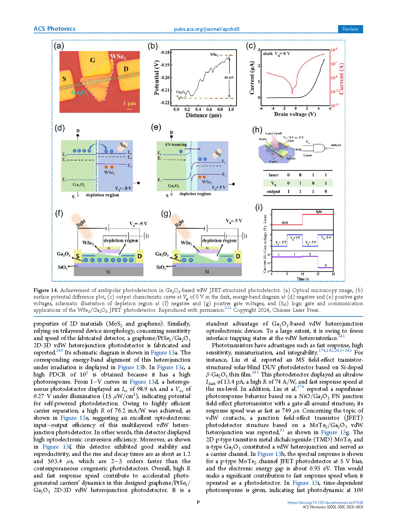
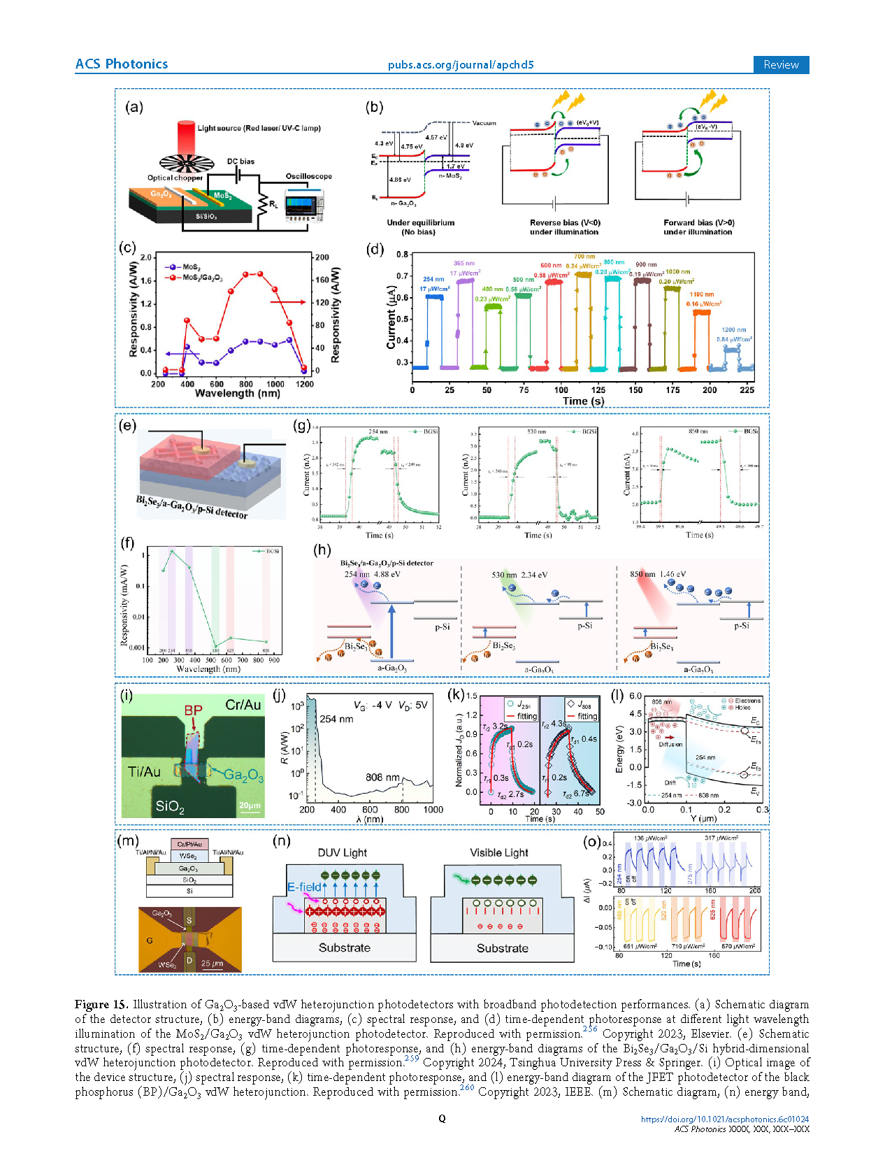
1.2D−3D hybrid heterostructures: The integration with 2D materials (e.g., graphene, MXene, and MoS₂) enables Fermi-level unpinning, accelerates photogenerated carrier dynamics, and realizes multifunctional capabilities such as ambipolar and broadband photodetection.
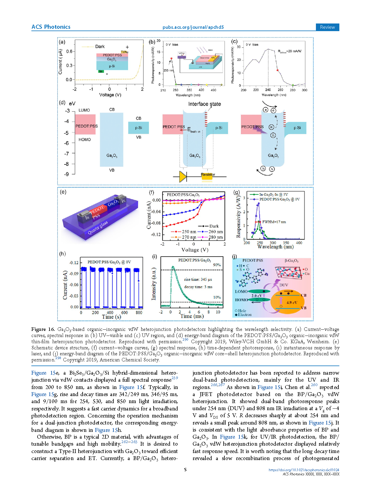
2.Organic−inorganic heterostructures: Incorporating organic layers (e.g., PEDOT:PSS) grants devices excellent wavelength selectivity and large V_oc, thereby maximizing the self-powered photoresponse.
3.vdW PN homojunctions: Ga₂O₃ faces a notorious p-type doping bottleneck. Constructing vdW homojunctions effectively bypasses this issue. This breakthrough pushes the boundaries for bipolar wide-bandgap optoelectronics.
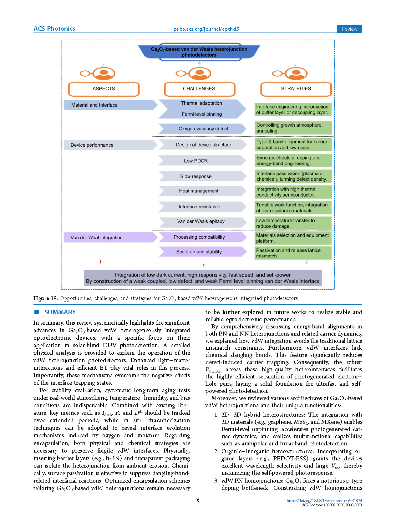
Despite the tremendous potential, bridging the gap between current laboratory research and practical applications faces several common challenges, as summarized in Figure 19. Future endeavors should be directed toward:
1.High-quality vdW epitaxy: Achieving large-area, high-quality vdW epitaxial growth remains a critical scientific challenge. This difficulty appears in both hetero- and homoepitaxy. Recent studies used graphene as a buffer layer to grow Ga₂O₃ on diamond substrates, which aimed at solving the heat dissipation problem. Meanwhile, other researchers constructed a near-vdW surface on the Ga₂O₃ (100) facet to achieve homoepitaxy. However, these breakthroughs have left behind some challenges. In heteroepitaxy, massive lattice and thermal mismatches still exist between the underlying materials. Achieving uniform nucleation and strict stress control over large-area graphene buffer layers remains very difficult. In homoepitaxy, the structural stability of the near-vdW surface on large wafers is hard to guarantee. The nondestructive exfoliation technique for high-quality epitaxial layers is also not yet fully mature. This severely limits the large-scale fabrication of flexible devices.
2.Comprehensive performance optimization: Breaking the performance trade-off is a major technical bottleneck. Devices struggle to simultaneously achieve low dark current, high responsivity, and fast response speed. This trade-off is deeply limited by internal oxygen vacancies and interface hole-trapping effects. Under DUV illumination, trapping centers capture numerous photogenerated holes. This provides a high photoelectric gain but severely delays the device recovery speed. Precisely controlling or eliminating trapping effects is difficult. Furthermore, devices are moving toward low-power neuromorphic computing and nonvolatile optoelectronic memory. Constructing multilayer vdW heterostructures (like MoS₂/Ga₂O₃/graphene) faces many unsolved problems. Achieving precise charge transfer control, stable multilevel conductance retention, and low operating energy consumption in such complex structures remains highly challenging.
Addressing these challenges will undoubtedly promote the practical deployment of Ga₂O₃-based vdW heterostructures in next-generation solar-blind DUV imaging, secure optical communications, environmental monitoring, and deep space exploration, boosting the development of integrated optics based on wide bandgap semiconductors (especially for Ga₂O₃).
Project Support
This work was supported by the National Natural Science Foundation of China (Grant Nos. 62564011, 62204125, U23A20349, 62305171, 62364014, and 62501320), the Young Scientists Fund (Type A) of the Natural Science Foundation of Inner Mongolia Autonomous Region of China (Grant No. 2026QA016), the Basic Scientific Research Funding for Universities Directly Affiliated with the Inner Mongolia Autonomous Region of China (Grant No. 2026JBKY002), the Inner Mongolia Autonomous Regionlevel Scientific Research Startup Fund (Grant Nos. 21700252904 and 21700-252905), the Steed Plan of Inner Mongolia University for Introducing High-Level Talents (Grant Nos. 10000-A24199006 and 10000-A24106015), the Inner Mongolia University Experimental Technology Research Project in 2026 (Self-Made and Modified Equipment Project) (Grant No. SYJS2026007), the Program for Innovative Research Team in Universities of Inner Mongolia Autonomous Region (Grant No. NMGIRT2503), and the Frontier Technologies R&D Program of Jiangsu (Grant No. BF202507).
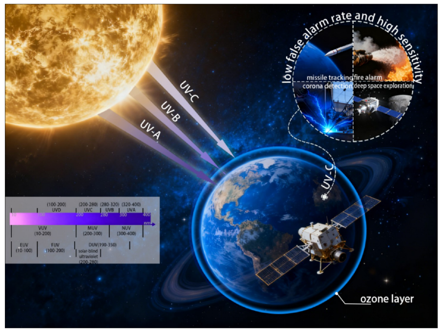
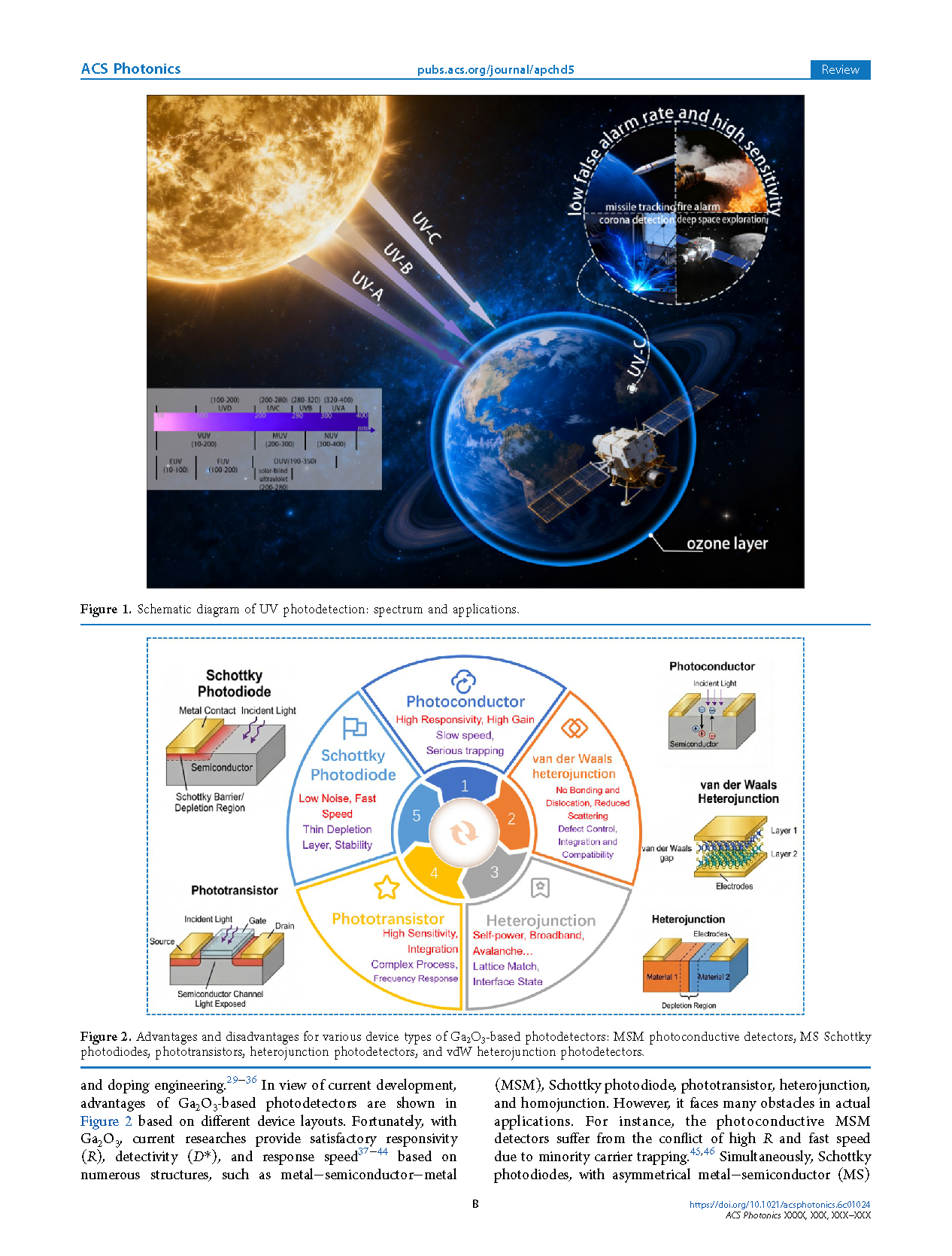
Figure 1. Schematic diagram of UV photodetection: spectrum and applications.
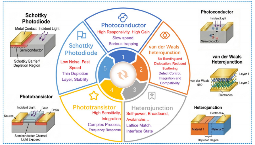
Figure 2. Advantages and disadvantages for various device types of Ga₂O₃-based photodetectors: MSM photoconductive detectors, MS Schottky photodiodes, phototransistors, heterojunction photodetectors, and vdW heterojunction photodetectors.
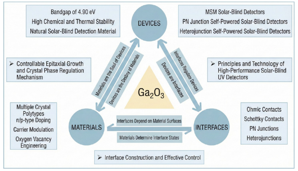
Figure 3. Researches on Ga₂O₃-based materials, devices and interfaces, and the inherent physical correlation.
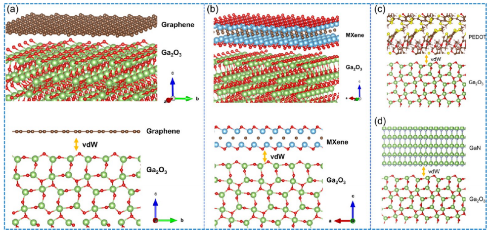
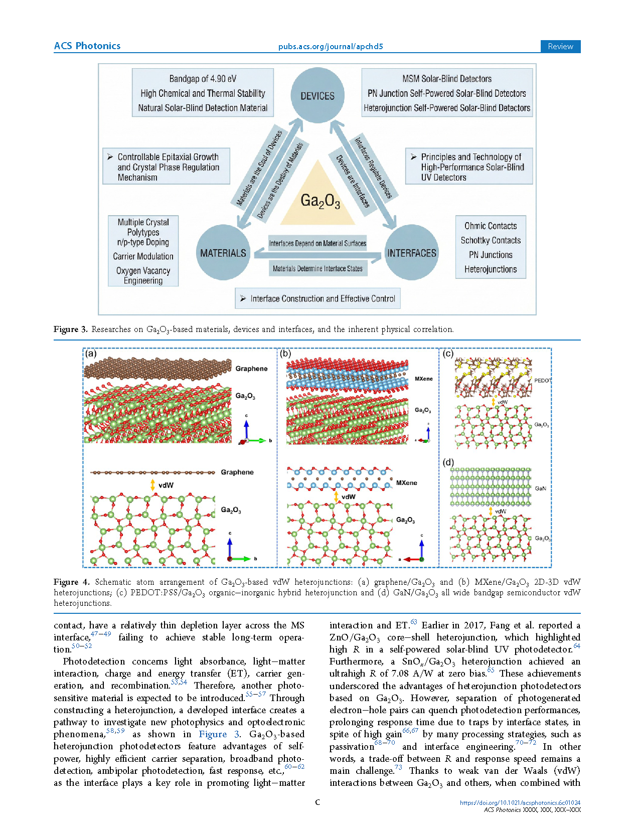
Figure 4. Schematic atom arrangement of Ga₂O₃-based vdW heterojunctions: (a) graphene/Ga₂O₃ and (b) MXene/Ga₂O₃ 2D-3D vdW heterojunctions; (c) PEDOT:PSS/Ga₂O₃ organic−inorganic hybrid heterojunction and (d) GaN/Ga₂O₃ all wide bandgap semiconductor vdW heterojunctions.
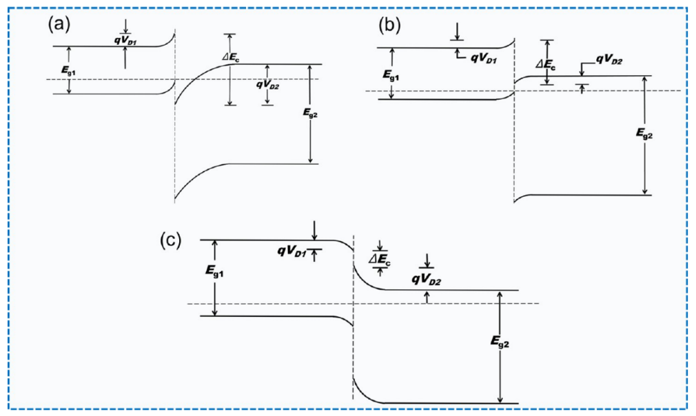
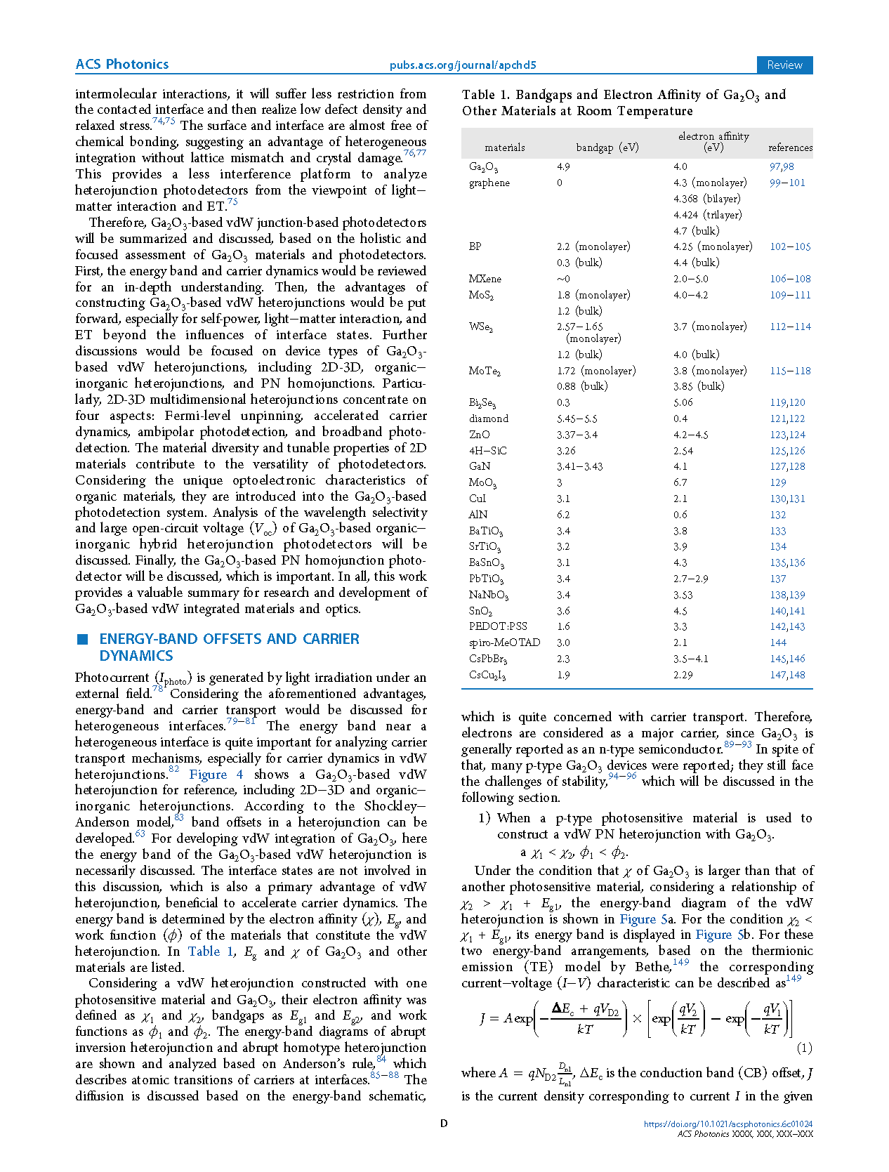
Figure 5. Schematic of energy-band alignments of the Ga₂O₃-based PN heterojunction when the electron affinity of Ga₂O₃ (χ₂) is larger than that of another material (χ₁). Ga₂O₃ is usually considered as an n-type semiconductor with a large bandgap.
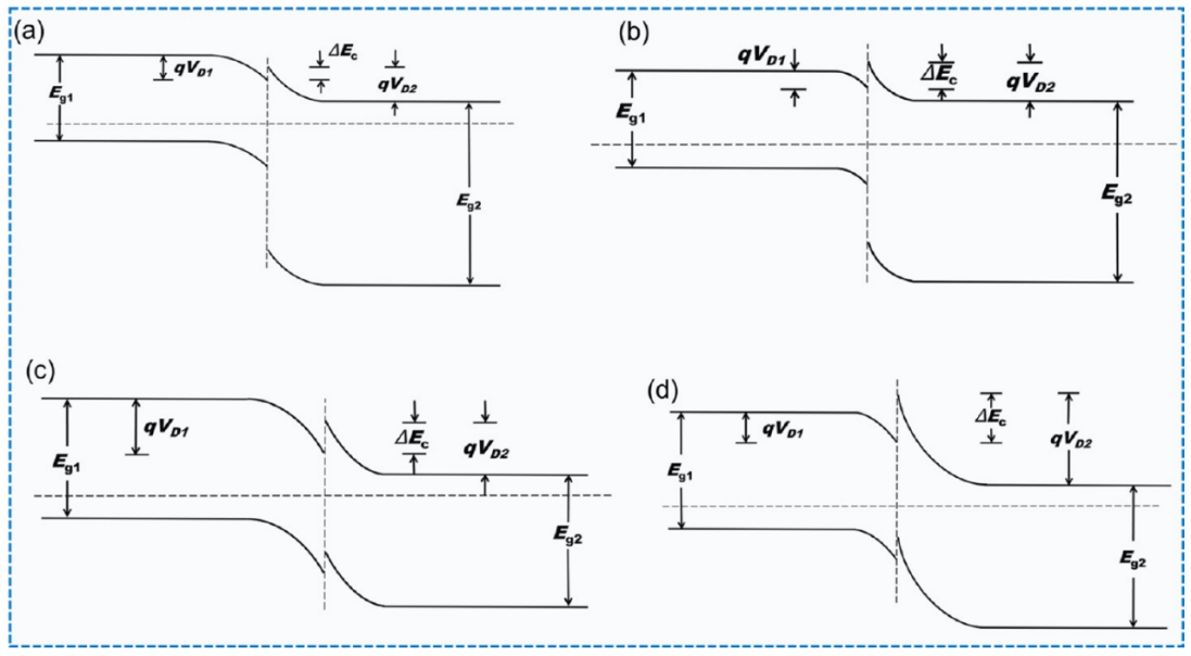
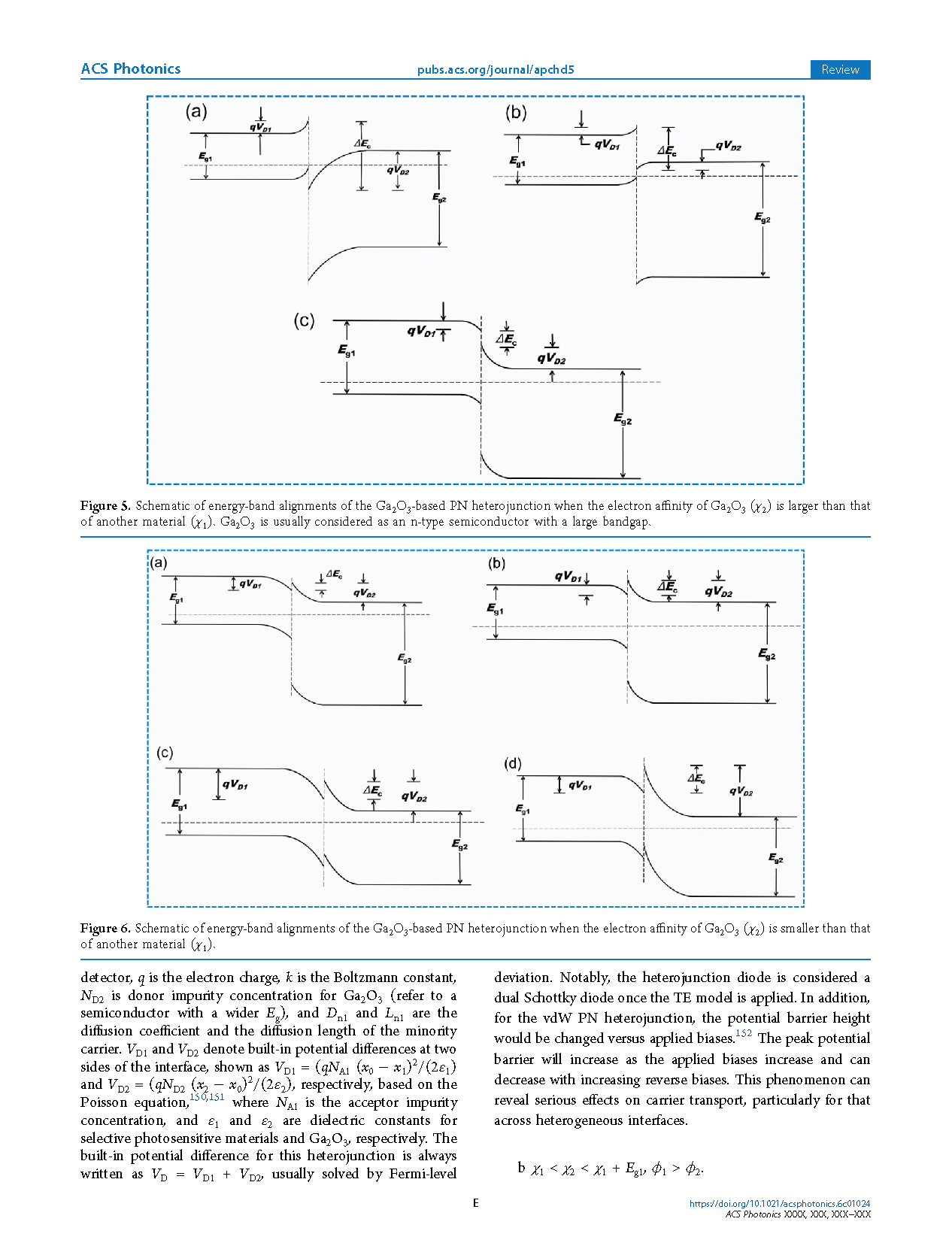
Figure 6. Schematic of energy-band alignments of the Ga₂O₃-based PN heterojunction when the electron affinity of Ga₂O₃ (χ₂) is smaller than that of another material (χ₁).
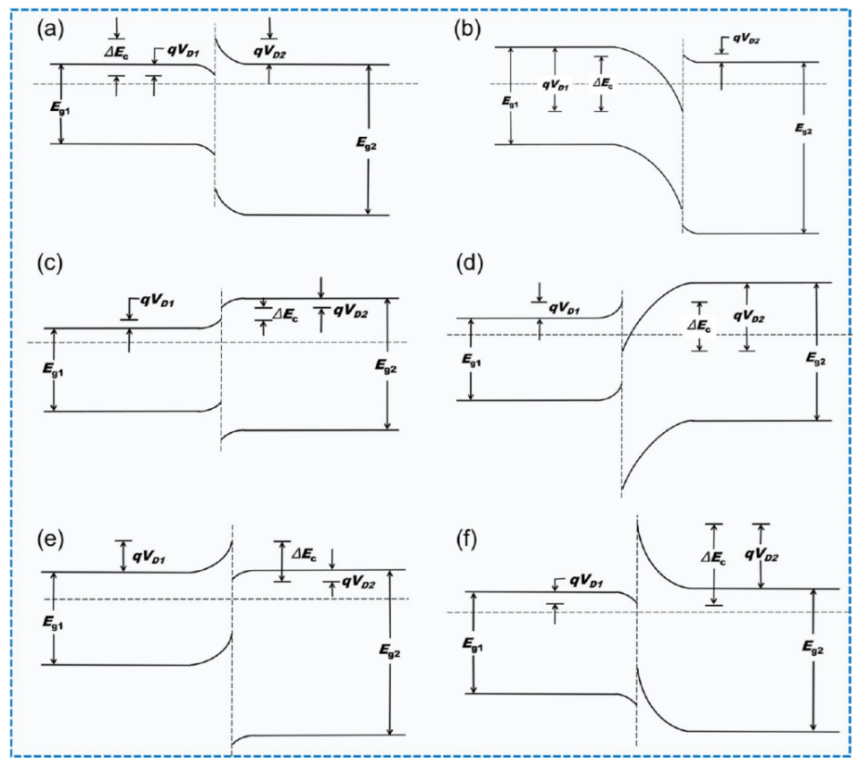
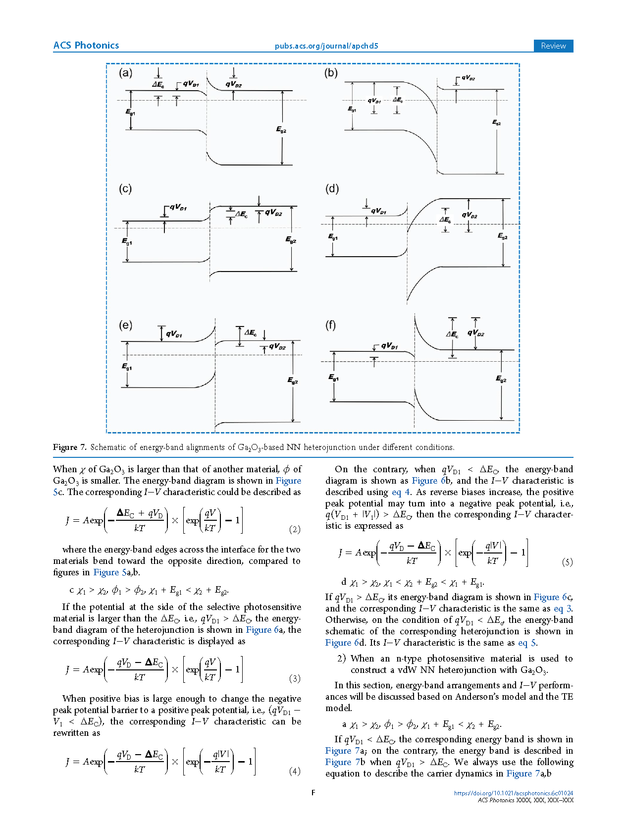
Figure 7. Schematic of energy-band alignments of Ga₂O₃-based NN heterojunction under different conditions.
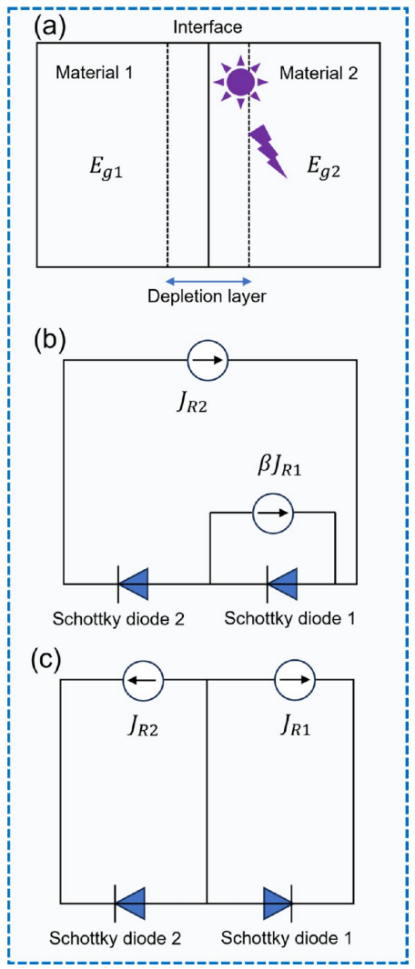
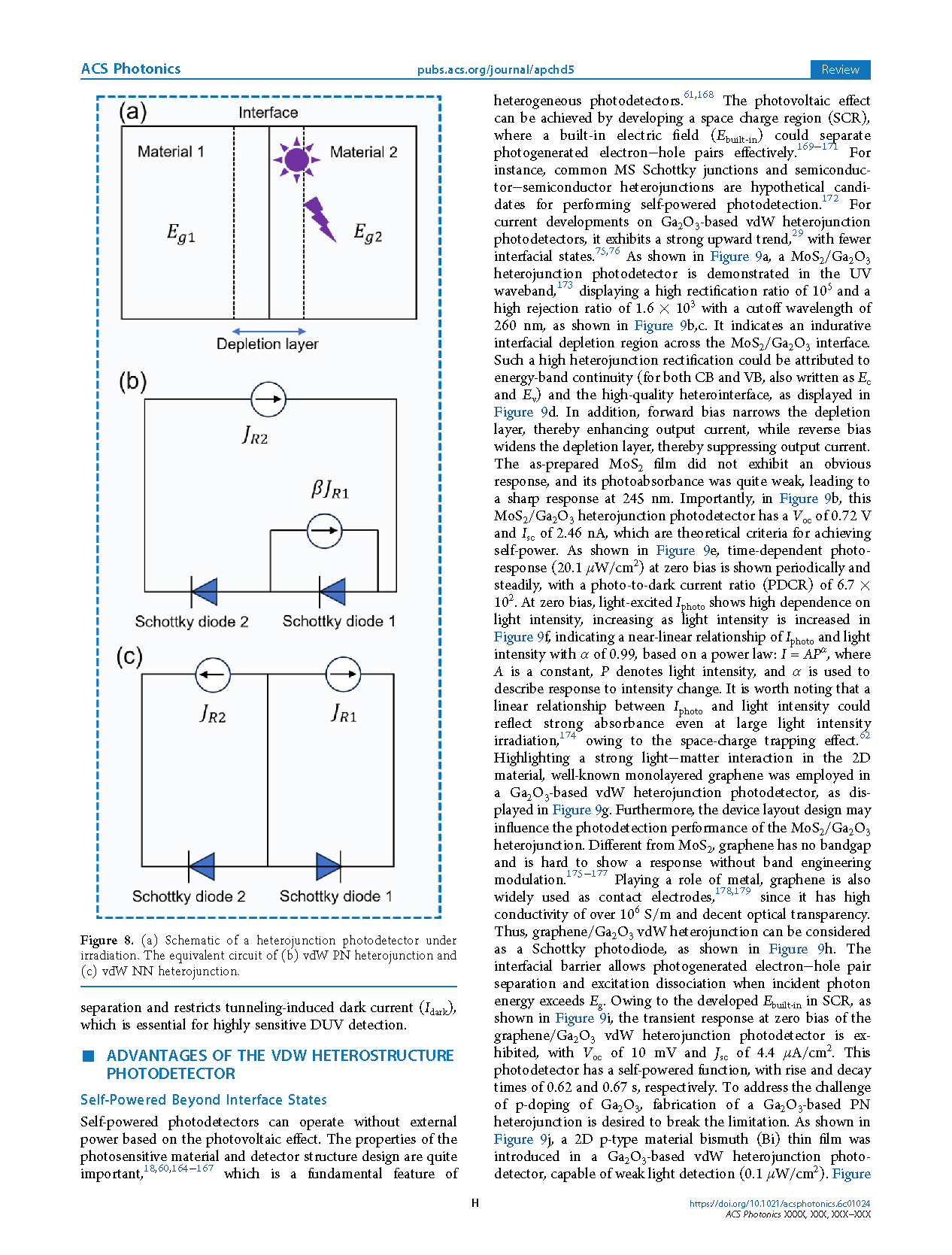
Figure 8. (a) Schematic of a heterojunction photodetector under irradiation. The equivalent circuit of (b) vdW PN heterojunction and (c) vdW NN heterojunction.
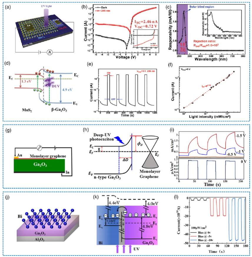
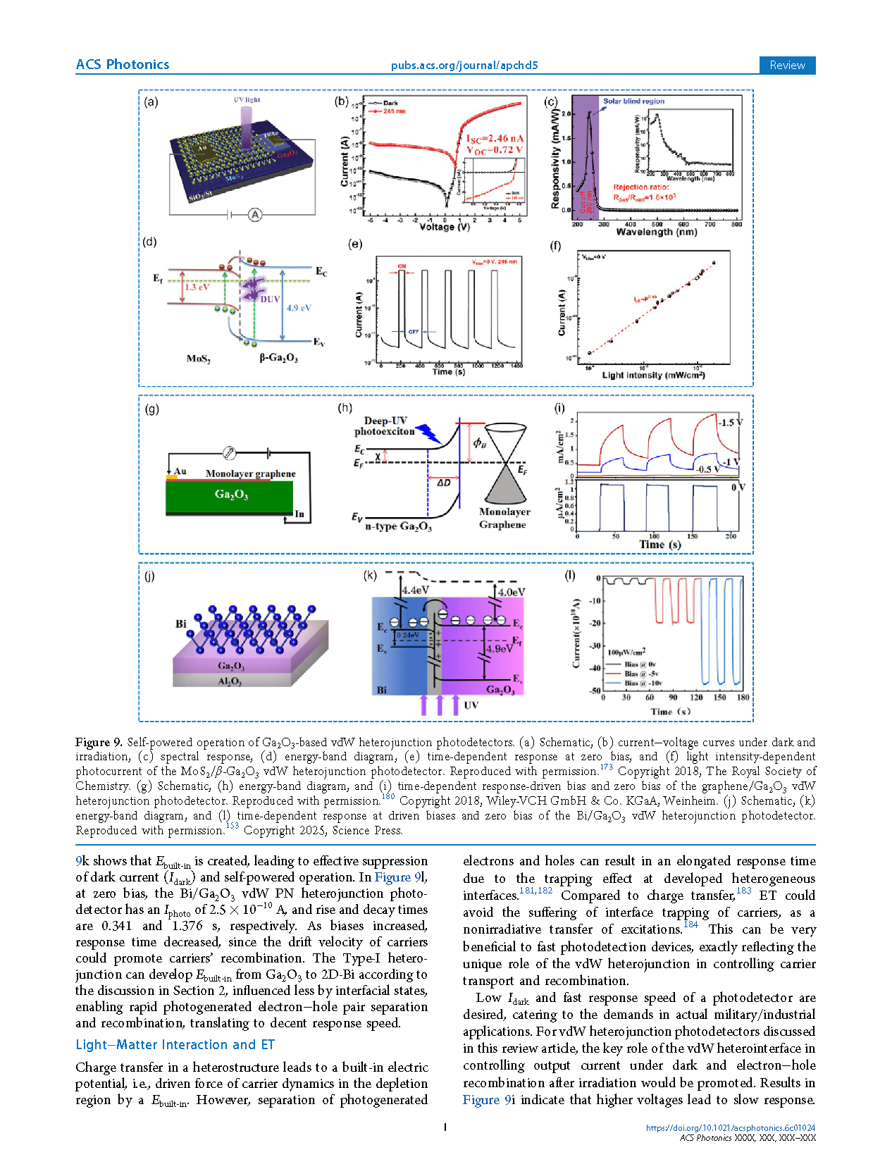
Figure 9.Self-powered operation of the MoS₂/Ga₂O₃ vdW heterojunction photodetector. (a) Schematic, (b) current−voltage curves under dark and irradiation, (c) spectral response, (d) energy-band diagram, (e) time-dependent response at zero bias, and (f) light intensity-dependent photocurrent of the MoS₂/β-Ga₂O₃ vdW heterojunction. (g) Schematic, (h) energy-band diagram, and (i) time-dependent response driven bias and zero bias of the graphene/Ga₂O₃ vdW heterojunction photodetector. (j) Schematic, (k) energy-band diagram, and (l) time-dependent response at driven biases and zero bias of the Bi/Ga₂O₃ vdW heterojunction photodetector.
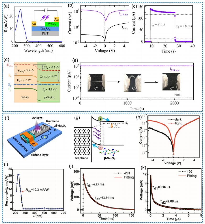
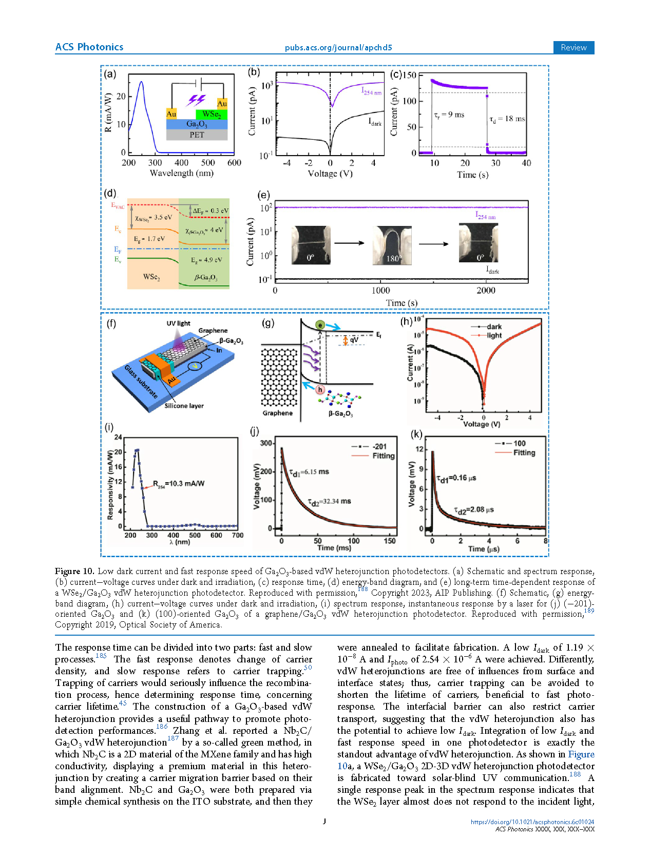
Figure 10.Low dark current and fast response speed of a WSe₂/Ga₂O₃ vdW heterojunction photodetector. (a) Schematic and spectrum response, (b) current−voltage curves under dark and irradiation, (c) response time, (d) energy-band diagram, and (e) long-term time-dependent response of a WSe₂/Ga₂O₃ vdW heterojunction photodetector. (f) Schematic, (g) energy-band diagram, (h) current−voltage curves, (i) spectrum response, instantaneous response by a laser for (j) (−201)-oriented Ga₂O₃ and (k) (100)-oriented Ga₂O₃ of a graphene/Ga₂O₃ vdW heterojunction photodetector.
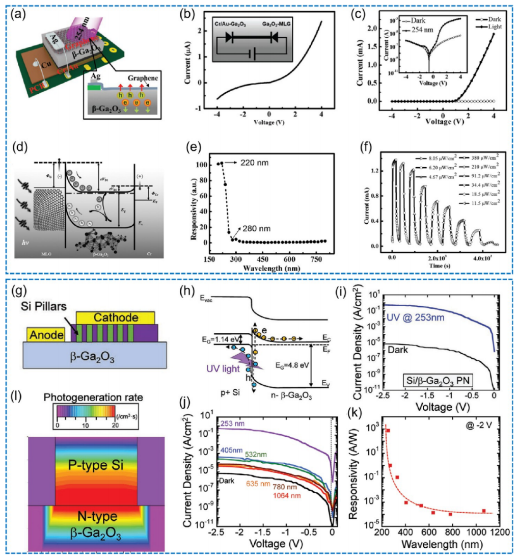
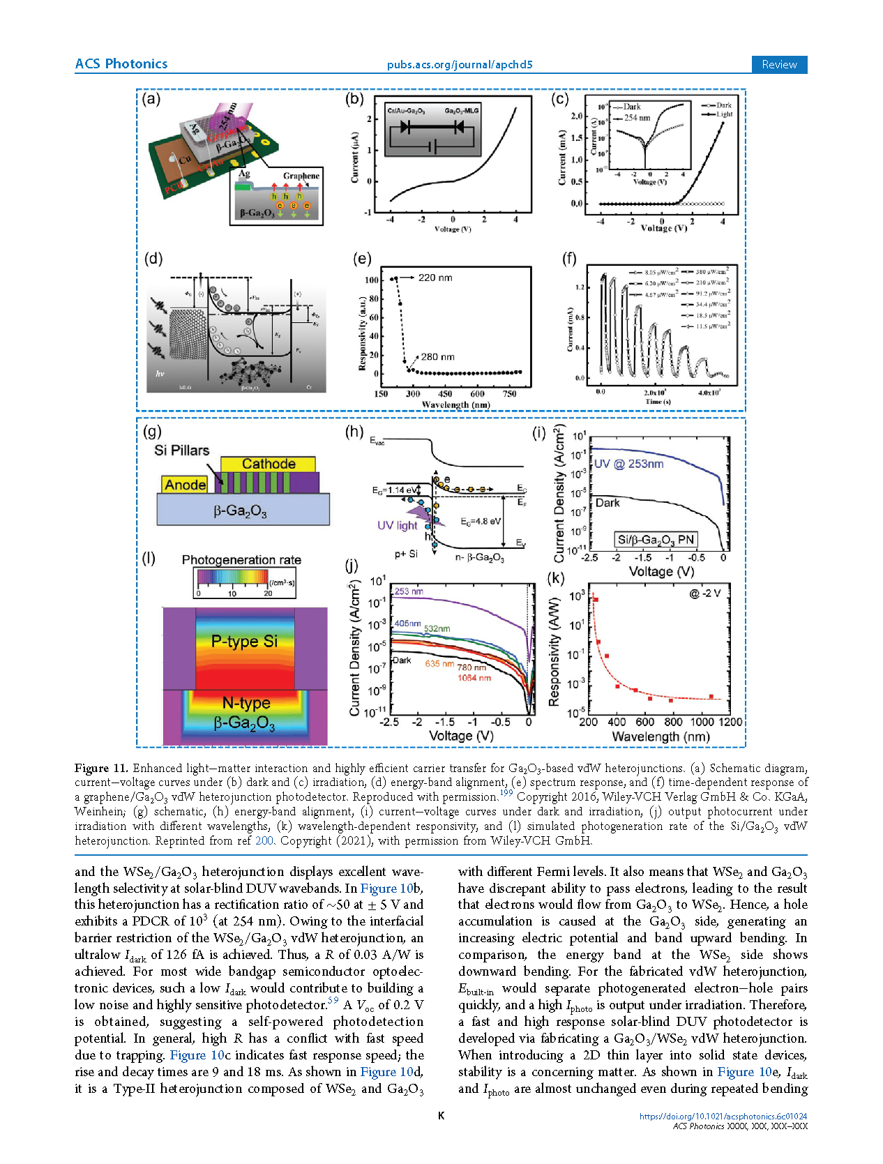
Figure 11.Enhanced light−matter interaction and highly efficient carrier transfer for graphene/Ga₂O₃ and Si/Ga₂O₃ vdW heterojunctions. (a) Schematic diagram, (b) current−voltage curves, (c) spectral response, (d) energy-band alignment, (e) spectrum response, and (f) time-dependent response of the graphene/Ga₂O₃ heterojunction. (g) Schematic, (h) energy-band diagram, (i) current−voltage curves, (j) output photocurrent under different wavelengths, (k) wavelength-dependent responsivity, and (l) simulated photogeneration rate of the Si/Ga₂O₃ vdW heterojunction.
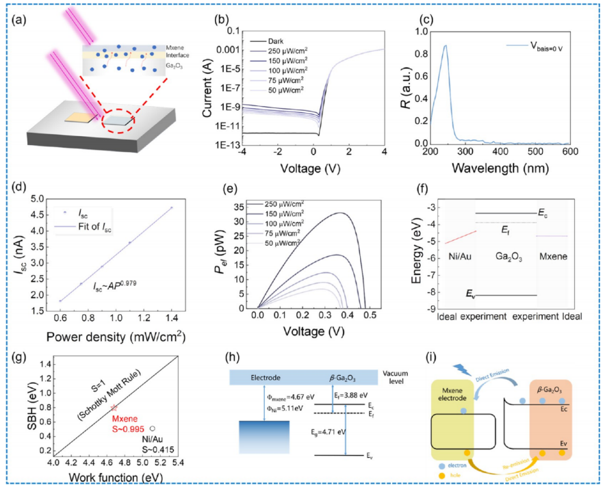
Figure 12.Fermi-level pinning-free MXene/Ga₂O₃ hybrid vdW heterojunction photodetector. (a) Schematic, (b) current−voltage curves under dark and irradiation, (c) spectral response, (d) light intensity-dependent short-circuit current, (e) output electrical power under different light intensities, (f) energy band of Ga₂O₃ with vdW contact, (g) SBH versus work functions, and (h,i) energy-band diagrams of the MXene/Ga₂O₃ vdW heterojunction photodetector.
DOI :
10.1021/acsphotonics.6c01024
Instruction
Official Account

Cooperation
Top
