


Researchers from the Xidian University have published a dissertation titled "Substrate Orientation-Dependent Domain Formation in Epitaxial NiO/β-Ga2O3 Heterostructures via Mist-CVD" in Journal of Alloys and Compounds.
Background
As an ultra-wide bandgap semiconductor, β-Ga₂O₃ possesses ultrahigh Baliga‘s figure of merit and a theoretical breakdown field of 8 MV/cm, which makes it a revolutionary candidate material for next-generation ultra-efficient power converters. Nevertheless, the intrinsic lack of stable and efficient p-type conductivity severely restricts the fabrication of high-performance homojunction p–n diodes and bipolar devices, which greatly limits the full exploitation of its power device potential.
Constructing heterojunctions between β-Ga₂O₃ and p-type oxides has become the mainstream technical route to break through this inherent limitation, among which p-type NiO exhibits outstanding application prospects. Since the first demonstration of NiO/β-Ga₂O₃ heterojunction diodes in 2016, this material system has realized breakdown voltages up to kilovolt level and ultra-low specific on-resistance, and its device performance can reach or even exceed that of conventional SiC and GaN power devices. Previous research mainly adopts high-energy vacuum deposition technologies including ALD, PLD and MBE combined with post-annealing treatment to adjust the non-stoichiometry of NiO films, so as to control hole concentration and reduce device leakage current.
However, three critical challenges still hinder the practical application of NiO/β-Ga₂O₃ heterojunctions. Firstly, polycrystalline NiO films contain massive grain boundaries, pores and oxygen vacancy point defects, which act as carrier trapping centers and localized leakage paths, degrading electrical performance and reliability. Secondly, even epitaxial NiO films generate rotational domains and domain boundaries, which aggravate carrier scattering and high-field leakage. Thirdly, thermal and electrical stress induces interdiffusion at the NiO/β-Ga₂O₃ interface, generating intermediate NiGa₂O₄ phases, resulting in band misalignment, increased leakage current and degraded breakdown characteristics.
Most existing deposition technologies are high-damage vacuum processes, which cannot fabricate high-quality single-crystalline NiO/β-Ga₂O₃ heterostructures with low defects and suppressed interdiffusion. Mist chemical vapor deposition (Mist-CVD) is an atmospheric-pressure low-damage growth method with precise stoichiometry control. At present, systematic research on how substrate orientation regulates the epitaxial domain configuration, interfacial quality and long-term electrical stability of NiO films is absent, which is the core research motivation of this paper.
Abstract
The interfacial configuration in oxide heteroepitaxy plays a critical role in determining the structural integrity and reliable performance of wide-bandgap heterostructures. Herein, we investigate the orientation-dependent epitaxial growth of high-quality NiO films on β-Ga₂O₃ via mist chemical vapor deposition (Mist-CVD), exhibiting distinct epitaxial domain configurations depending on the substrate orientation. Combined experimental and density functional theory (DFT) analyses reveal that the synergistic interplay among surface energy, lattice mismatch, and crystal symmetry governs the epitaxial mode and crystalline quality across different substrate orientations. Benefiting from the high-quality epitaxy, the NiO films demonstrate good environmental stability, retaining 94% of their initial current after 30 days of ambient exposure. As a functional demonstration, the NiO/(001) β-Ga₂O₃ p-n diode exhibits a low leakage current density (2.08 ×10⁻⁸ A·cm⁻² @-100 V) and a high breakdown voltage of 885 V, highlighting the critical role of epitaxial interface quality. This study provides mechanistic insight into orientation-regulated oxide heteroepitaxy and offers a viable materials strategy for constructing stable wide-bandgap oxide heterostructures.
Highlights
The vacuum-free, low-damage Mist-CVD technology is utilized to achieve the epitaxial growth of high-quality single-crystalline NiO thin films on β-Ga₂O₃substrates with diverse orientations. This work systematically elucidates the inherent law that substrate orientation regulates the epitaxial domain structure of NiO for the first time.
Combined with XRD pole figure characterization, TEM strain mapping and DFT theoretical calculations, this study reveals that the synergistic interaction of surface energy, lattice mismatch and crystal symmetry collectively governs the epitaxial growth mode and crystalline quality of NiO films.
Single-crystalline NiO films grown via Mist-CVD possess excellent environmental stability, and their leakage current degradation is significantly suppressed compared with sputtered polycrystalline NiO. The vertical p-n heterojunction diodes built on (001) β-Ga₂O₃deliver ultra-low reverse leakage current and a high breakdown voltage of 885 V, with a power figure of merit reaching 0.308 GW/cm².
A universal strategy for orientation-tuned oxide heteroepitaxy is put forward, which offers a novel idea for the controllable preparation of wide-bandgap heterostructures consisting of other functional oxides.
Conclusion
In summary, this study demonstrates the successful epitaxial growth of high-quality single crystalline NiO thin films on β-Ga₂O₃ substrates via Mist-CVD method. Among the obtained films, the (111) NiO grown on (-201) β-Ga₂O₃ exhibits the highest crystalline quality, as reflected by a narrow rocking curve FWHM of 0.031°. A combination of systematic structural characterization and density functional theory calculations confirm that the synergistic interplay among surface energy, lattice mismatch, and crystal symmetry serves as the internal factors governing the precise regulation of both the epitaxial mode and crystalline quality of NiO on differently oriented β-Ga₂O₃ substrates. Benefiting from the high-quality epitaxial structure, the NiO films show excellent environmental stability, with CTLM devices maintaining stable performance even under harsh conditions. Furthermore, the NiO/(001) β-Ga₂O₃ p–n diode fabricated from these films demonstrates a high breakdown voltage and a low leakage current, underscoring its potential for power-electronics applications. This work not only confirms the powerful capability of the mist-CVD technique in preparing high-performance single-crystalline oxide films and its excellent compatibility with existing processes, but also provides a universal strategy for the epitaxial growth of other functional oxide films.
Project Support
This work was supported by the National Natural Science Foundation of China (No. 62274132), the National Key R&D Program of China (No. 2022YFB3605402), the Innovation Fund of Xidian University (YJSJ25013), and the Fundamental and Interdisciplinary Disciplines Breakthrough Plan of the Ministry of Education of China (JYB2025XDXM406).
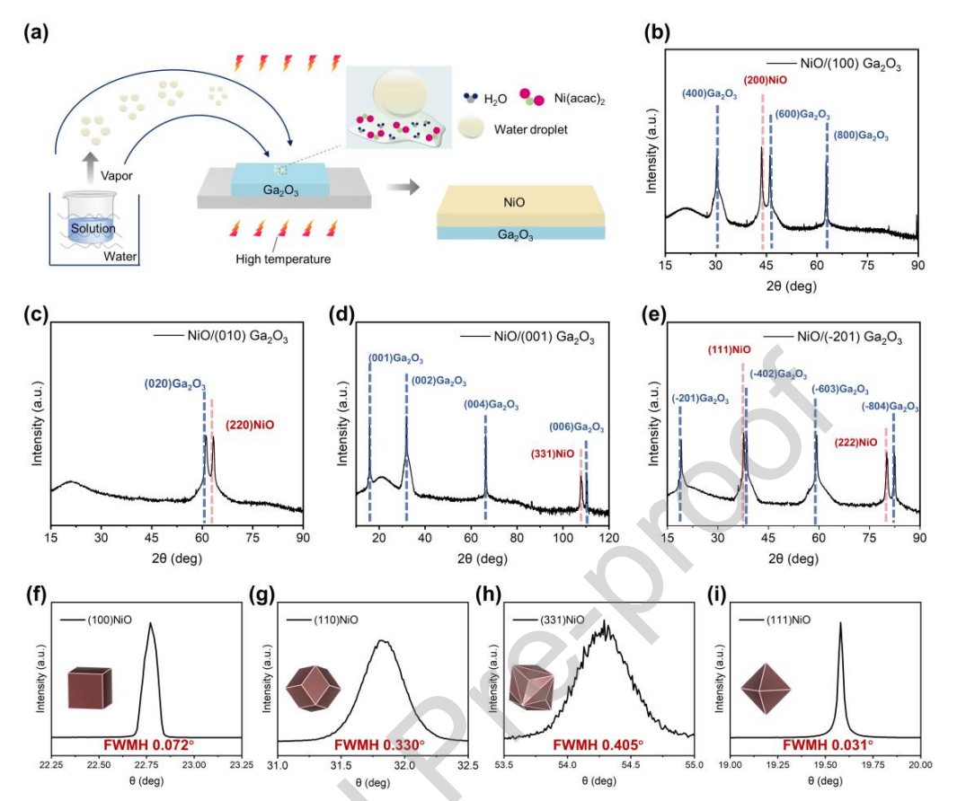
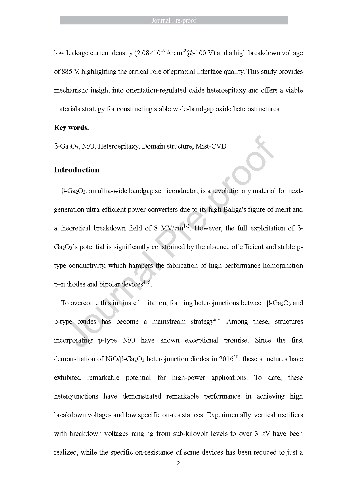
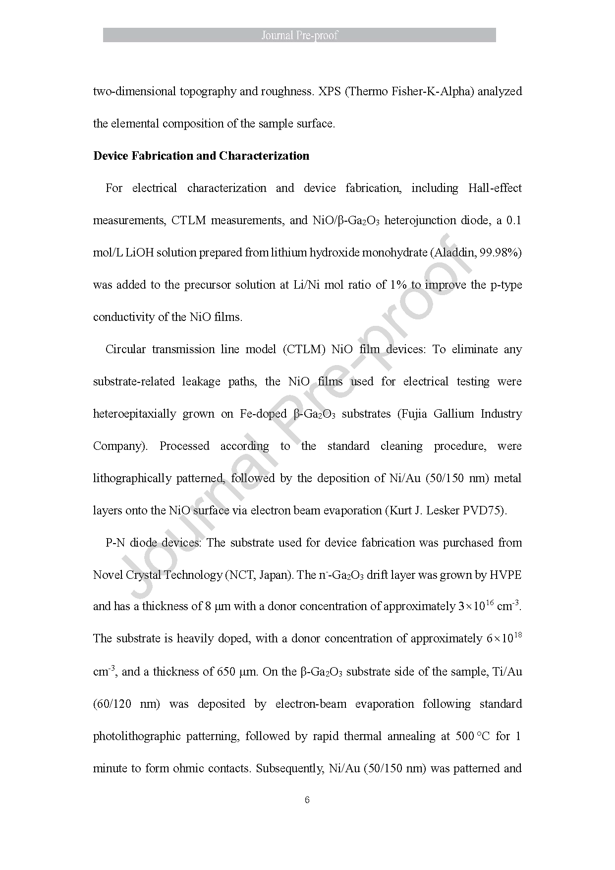
Fig. 1 (a) Schematic diagram of the Mist-CVD growth process. XRD patterns of (b) NiO/(100) Ga₂O₃, (c) NiO/(010) Ga₂O₃, (d) NiO/(001) Ga₂O₃ and (e) NiO/(-201) Ga₂O₃. The FWHM of NiO films on (f) (100), (g) (010), (h) (001) and (-201) Ga₂O₃ substrates. (Inset: a schematic diagram of the structure corresponding to the NiO crystal orientation.)

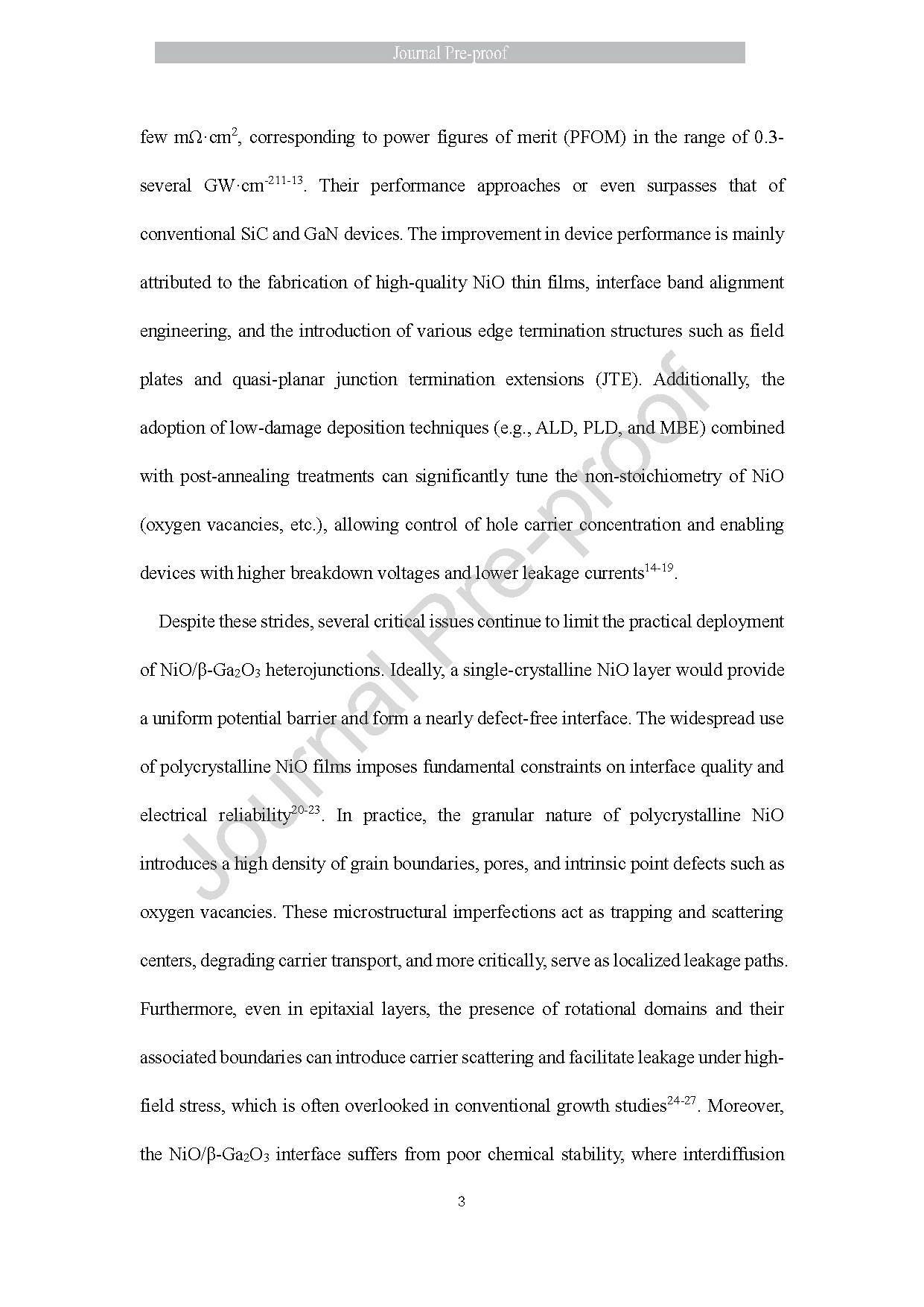
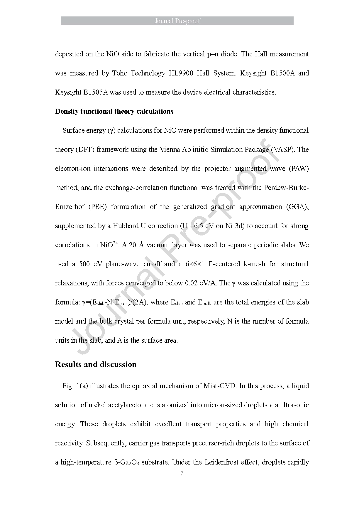
Fig. 2 Cross-sectional TEM of (a) (100) NiO/(100) Ga₂O₃, (b) (110) NiO/(010) Ga₂O₃, (c) (111) NiO/(-201) Ga₂O₃, (d) (331) NiO/(001) Ga₂O₃, (Inset: the electron diffraction of NiO layer (upper right corner) and Ga₂O₃ layer (lower right corner). (e) Large scale TEM of (331) NiO/(001) Ga₂O₃ (f) The strain fields of surface NiO and interface NiO, the left column shows the in-plane strain, and the right column represents the out-of-plane strain. (g) Schematic illustrations of the NiO lattice with {100} and (331) orientations. (h) φ-scans of NiO films on (001) Ga₂O₃ substrate (NiO 220 reflection). (i) Schematic diagram of the epitaxial growth of NiO thin films on (001) Ga₂O₃ substrate.
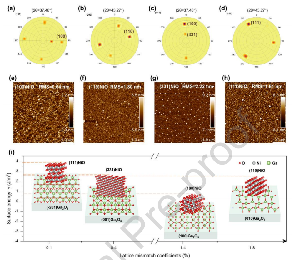
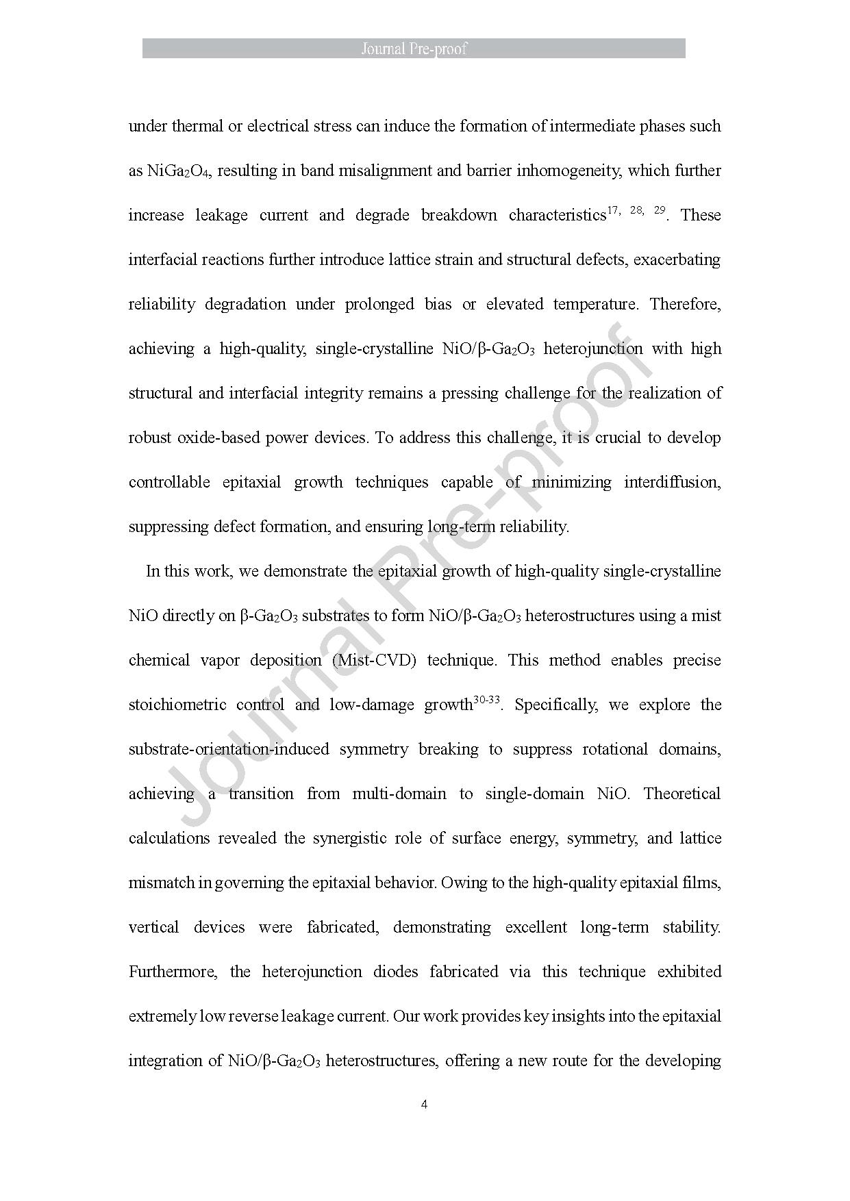
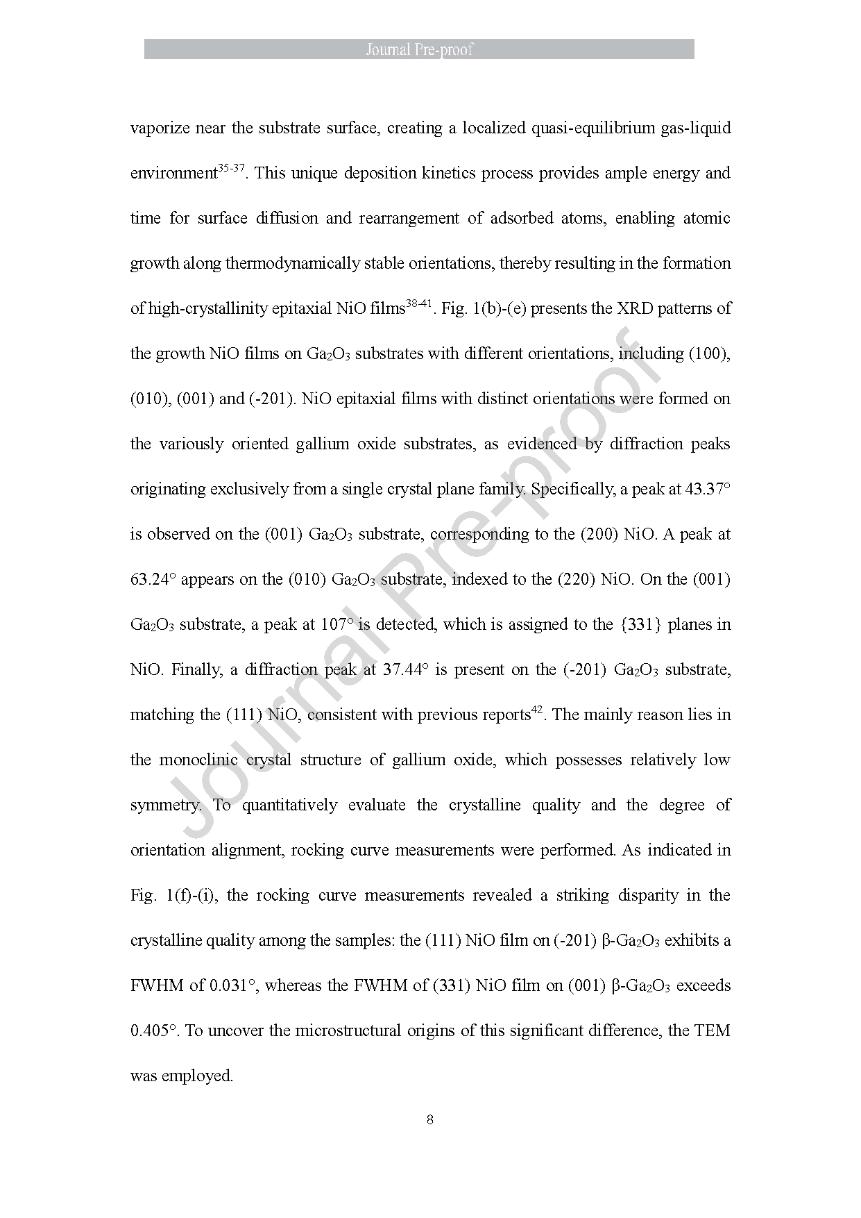
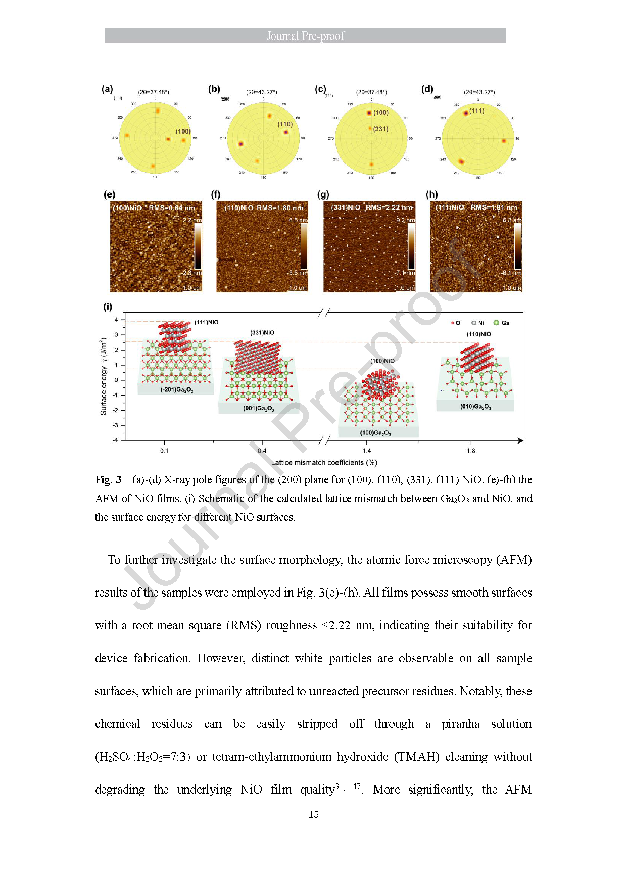
Fig. 3 (a)-(d) X-ray pole figures of the (200) plane for (100), (110), (331), (111) NiO. (e)-(h) the AFM of NiO films. (i) Schematic of the calculated lattice mismatch between Ga₂O₃ and NiO, and the surface energy for different NiO surfaces.
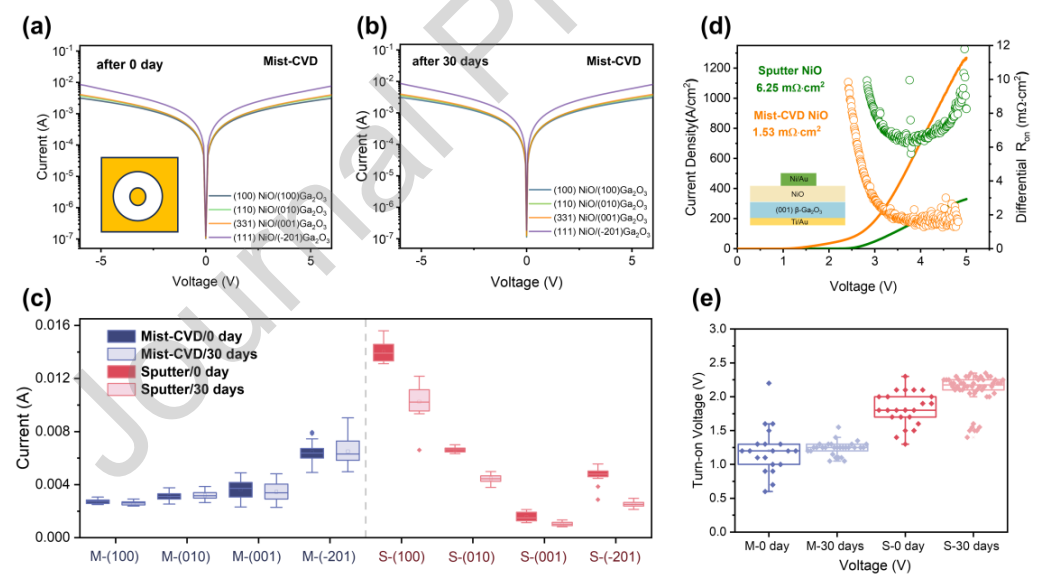
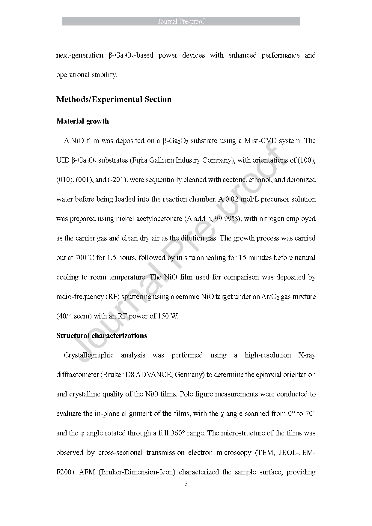
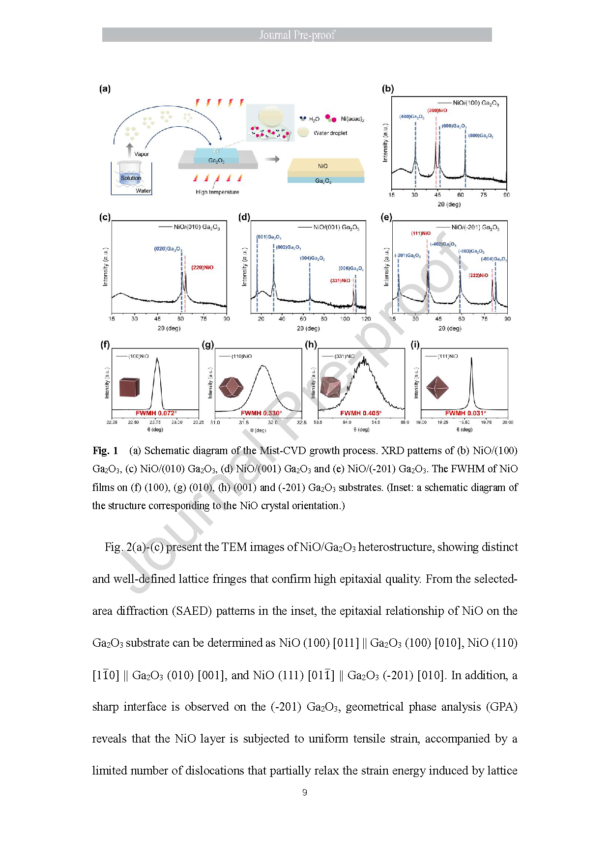
Fig. 4 Superior electrical stability of NiO films grown by mist-CVD. (a) Initial and (b) aged 30 days I-V characteristics of NiO film (Inset: schematic diagram of CTLM structure). (c) Statistical comparison of the current (at 5 V) for NiO CTLM devices on (100), (010), (001), and (-201) Ga₂O₃ substrates fabricated by mist-CVD and sputtering, before and after aging (50% relative humidity, 27°C). (d) J-V characteristics of the NiO/(001) Ga₂O₃ heterojunction via Mist-CVD and Sputtering. (e) Turn-on voltages statistics of NiO/(001) Ga₂O₃ heterojunction prepared by mist-CVD and sputtering.
DOI :
10.1016/j.jallcom.2026.189821
Instruction
Official Account

Cooperation
Top
