


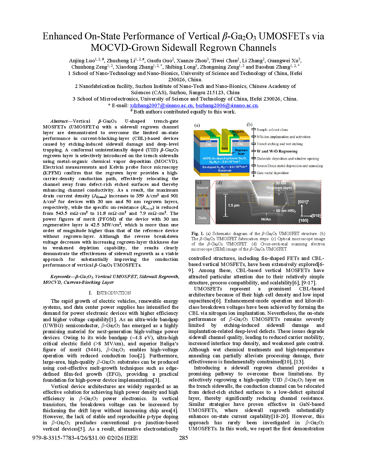
Researchers from the University of Science and Technology of China have published a paper titled " Enhanced On-State Performance of Vertical β-Ga2O3 UMOSFETs via MOCVD-Grown Sidewall Regrown Channels " in 2026 IEEE 38th International Symposium on Power Semiconductor Devices and ICs.
Background
The large-scale application of electric vehicles, renewable energy storage systems and data center power supply modules has rapidly boosted the demand for power semiconductor devices with low loss and high breakdown voltage in the power electronics industry. As an ultra-wide bandgap semiconductor, β-Ga₂O₃ has an intrinsic bandgap of approximately 4.8 eV, a critical breakdown electric field over 8 MV/cm, and Baliga’s figure of merit of 3444, which far outperforms commercial power semiconductors such as silicon, silicon carbide and gallium nitride, enabling drastically reduced conduction loss under high-voltage operating conditions. Meanwhile, the edge-defined film-fed growth (EFG) melt growth technology can fabricate large-size single-crystal β-Ga₂O₃ substrates with high crystalline quality at low cost, laying a material foundation for the industrialization of high-power devices.
Vertical device architecture is the optimal solution for β-Ga₂O₃ power chips to achieve high power density and high conversion efficiency, as the breakdown voltage can be improved by thickening the drift layer without enlarging the chip area. However, stable and repeatable p-type doping cannot be realized in β-Ga₂O₃, making it impossible to fabricate traditional vertical power devices based on p-n junctions. Therefore, electrostatically controlled devices including fin-shaped FETs and vertical MOSFETs with current-blocking layer (CBL) have been extensively studied. Among them, vertical U-shaped trench-gate MOSFETs (UMOSFETs) with CBL formed by nitrogen ion implantation have attracted widespread attention due to simple process flow and excellent scalability, and such devices can operate in enhancement mode with kilovolt-class breakdown voltage.
Nevertheless, conventional CBL-based β-Ga₂O₃ UMOSFETs face critical limitations: trench etching introduces severe lattice damage on sidewalls, and ion implantation generates abundant deep-level trap defects simultaneously. These two factors degrade channel interface quality, resulting in reduced carrier mobility, elevated interface trap density and weakened gate control capability. Wet chemical cleaning and high-temperature annealing can only partially repair process-induced damage with limited optimization effects.
Drawing on the sidewall epitaxial regrowth strategy applied in gallium nitride trench MOSFETs, selectively regrowing high-quality unintentionally doped epitaxial layers on trench sidewalls can shift the conductive channel from damaged etched surfaces to low-defect epitaxial films and drastically cut channel resistance. However, this sidewall regrowth scheme has rarely been investigated in β-Ga₂O₃ UMOSFETs. In this work, metal–organic chemical vapor deposition (MOCVD) is adopted to grow unintentionally doped β-Ga₂O₃ regrown layers on trench sidewalls, and the improvement of device on-state performance brought by the regrown layers is systematically studied.
Abstract
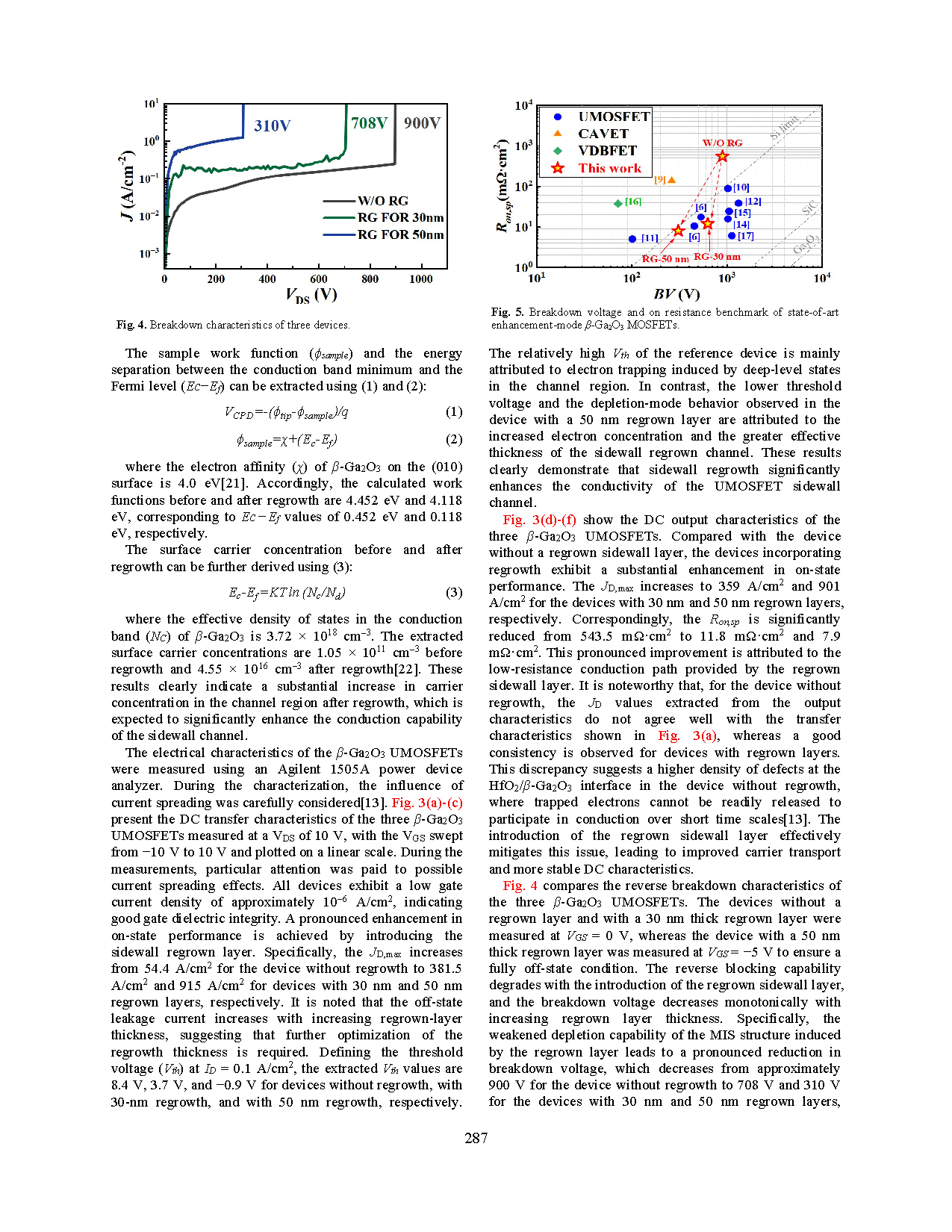
Vertical β-Ga₂O₃ U-shaped trench-gate MOSFETs (UMOSFETs) with a sidewall regrown channel layer are demonstrated to overcome the limited on-state performance in current-blocking-layer (CBL)-based devices caused by etching-induced sidewall damage and deep-level trapping. A conformal unintentionally doped (UID) β-Ga₂O₃ regrown layer is selectively introduced on the trench sidewalls using metal–organic chemical vapor deposition (MOCVD). Electrical measurements and Kelvin probe force microscopy (KPFM) confirm that the regrown layer provides a high-carrier-density conduction path, effectively relocating the channel away from defect-rich etched surfaces and thereby enhancing channel conductivity. As a result, the maximum drain current density (JD,max) increases to 359 A/cm² and 901 A/cm² for devices with 30 nm and 50 nm regrown layers, respectively, while the specific on-resistance (Ron,sp) is reduced from 543.5 mΩ·cm² to 11.8 mΩ·cm² and 7.9 mΩ·cm². The power figures of merit (PFOM) of the device with 30 nm regenerative layer is 42.5 MW/cm², which is more than one order of magnitude higher than that of the reference device without regrown-layer. Although the reverse breakdown voltage decreases with increasing regrown-layer thickness due to weakened depletion capability, the results clearly demonstrate the effectiveness of sidewall regrowth as a viable approach for substantially improving the conduction performance of vertical β-Ga₂O₃ UMOSFETs.
Highlights
For the first time, a selective MOCVD sidewall regrowth strategy of unintentionally doped β-Ga₂O₃channel layer is proposed and verified to address the limited on-state performance of conventional CBL-based β-Ga₂O₃ UMOSFETs originating from etching-induced sidewall damage and deep-level traps.
KPFM characterization quantitatively proves that the regrown layer drastically elevates surface carrier concentration on trench sidewalls, shifts conductive channels from defect-abundant etched surfaces to low-defect epitaxial films and establishes low-resistance conduction paths.
Devices with 30 nm and 50 nm regrown layers are fabricated, achieving remarkable enhancement of drain current density and an order-of-magnitude reduction in specific on-resistance; the power figure of merit of the 30 nm-regrown device is over one order higher than that of the reference device without regrown layer.
The trade-off between regrown layer thickness and reverse breakdown voltage is experimentally clarified, providing experimental guidance for subsequent device optimization balancing conduction and blocking performance.
The sidewall regrowth process is scalable, offering a novel feasible technical route for high-performance vertical β-Ga₂O₃ power devices.
Conclusion
In conclusion, a sidewall regrowth strategy has been demonstrated to effectively enhance the on-state performance of CBL-based vertical β-Ga₂O₃ UMOSFETs. By introducing a conformal UID β-Ga₂O₃ regrown layer on the trench sidewalls using MOCVD, the conduction channel is reconstructed away from defect-rich etched regions, resulting in significantly improved current capability and reduced on-resistance. Although a trade-off between conduction performance and breakdown voltage is observed, the results clearly establish sidewall regrowth as a viable and scalable approach for overcoming the conduction limitations of vertical β-Ga₂O₃ UMOSFETs. By further optimizing the thickness and material quality of the regeneration layer, combined with advanced electric field management techniques, the device is expected to achieve more balanced performance in high-voltage power applications.
Project Support
This work was supported in part by the Funded by Basic Research Program of Jiangsu (Grant No. BK20253003), in part by the Suzhou Critical Core Technology Research Project (Grant No. SYG2024003). The authors would like to thank Nano Fabrication Facility and Vacuum Interconnected Nanotech Workstation (NANO-X) of Suzhou Institute of Nano-Tech and Nano-Bionics, Chinese Academy of Sciences for their technical support.
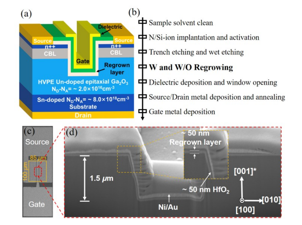
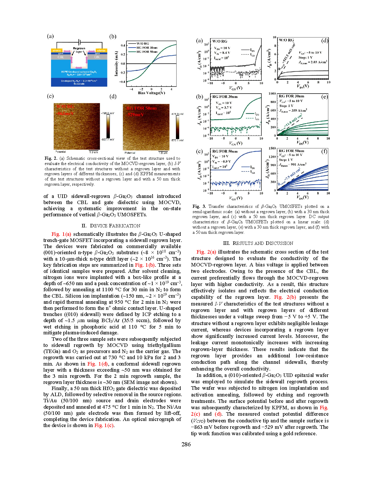
Fig. 1. (a) Schematic diagram of the β-Ga₂O₃ UMOSFET structure. (b) The β-Ga₂O₃ UMOSFET fabrication steps. (c) Optical microscope image of the β-Ga₂O₃ UMOSFET. (d) Cross-sectional scanning electron microscope (SEM) image of the β-Ga₂O₃ UMOSFET.
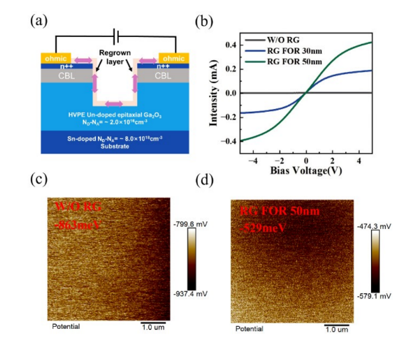
Fig. 2. (a) Schematic cross-sectional view of the test structure used to evaluate the electrical conductivity of the MOCVD-regrown layer, (b) I-V characteristics of the test structures without a regrown layer and with regrown layers of different thicknesses, (c) and (d) KPFM measurements of the test structures without a regrown layer and with a 50 nm thick regrown layer, respectively.
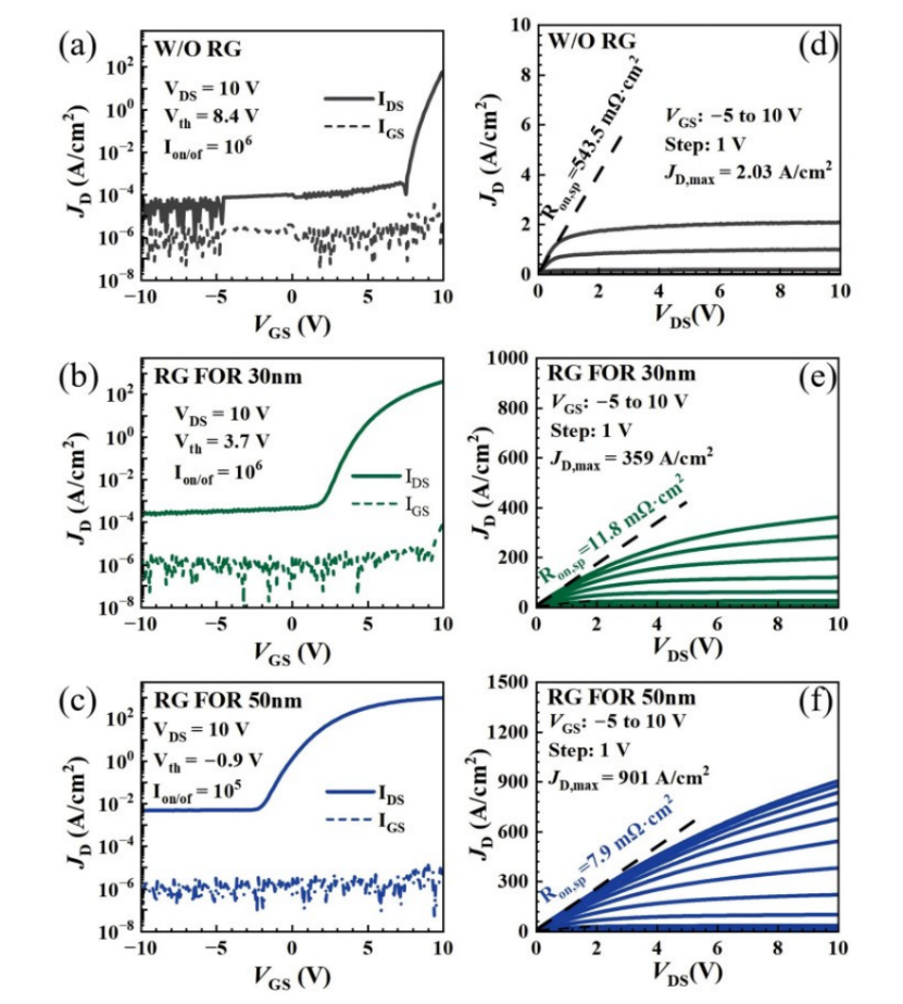
Fig. 3. Transfer characteristics of β-Ga₂O₃ UMOSFETs plotted on a semilogarithmic scale: (a) without a regrown layer, (b) with a 30 nm thick regrown layer, and (c) with a 50 nm thick regrown layer. DC output characteristics of β-Ga₂O₃ UMOSFETs plotted on a linear scale: (d) without a regrown layer, (e) with a 30 nm thick regrown layer, and (f) with a 50 nm thick regrown layer.
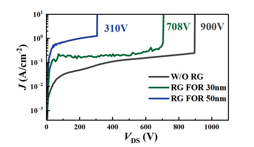
Fig. 4. Breakdown characteristics of three devices.
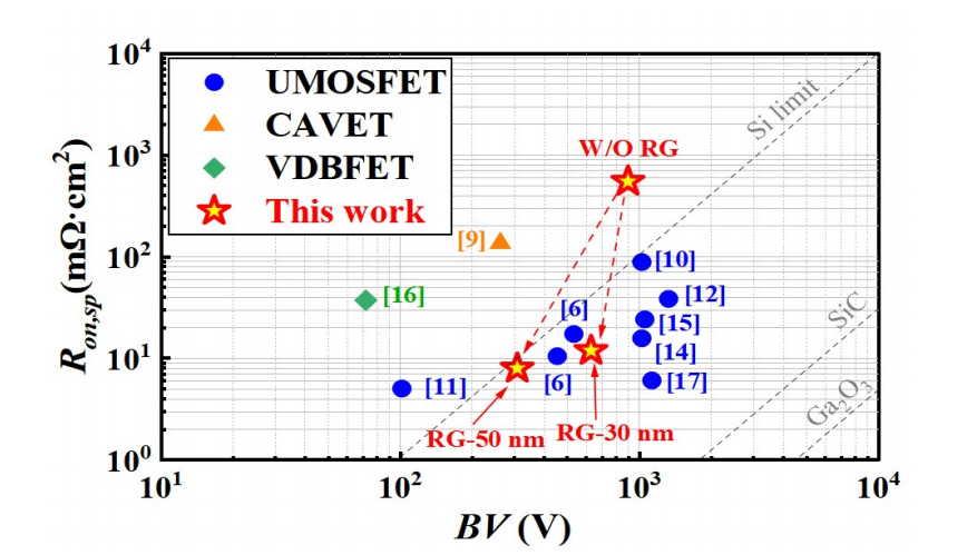
Fig. 5. Breakdown voltage and on resistance benchmark of state-of-art enhancement-mode β-Ga₂O₃ MOSFETs.
DOI:
10.1109/ISPSD64561.2026.11553761
Instruction
Official Account

Cooperation
Top
