


Researchers from Sun Yat-sen University, Suzhou Institute of Nano-Tech and Nano-Bionics (Chinese Academy of Sciences), University of Macau and The Hong Kong University of Science and Technology have published a paper titled “1.4 kV β-Ga₂O₃ VDMOSFET with high-temperature nitrogen-implanted current blocking layer” in Science China Information Sciences.
Background
β-Ga₂O₃ is an ultrawide bandgap semiconductor with a bandgap of ~ 4.8 eV, ultrahigh critical breakdown field of ~ 8 MV/cm and outstanding Baliga’s figure of merit. Low-cost large-area single crystal substrates grown by melt method make it a core candidate for next-generation high-voltage power electronics. Vertical MOSFET architectures boost breakdown voltage and power density by increasing drift layer thickness, and enhancement-mode devices feature inherent fail-safe property. However, stable p-type doping cannot be realized in β-Ga₂O₃, which hinders the development of vertical E-mode transistors. Fin-channel devices suffer lattice damage and degraded MOS interfaces from deep etching. Deep-level nitrogen ion implantation can form quasi-p-type current blocking layer (CBL) to fabricate vertical devices such as CAVET and UMOS, yet these devices suffer excessive leakage and premature breakdown. Vertical double-implanted MOSFET (VDMOS) is widely adopted in SiC, whose planar gate mitigates electric field crowding and avoids trench reliability issues, without trade-off between threshold voltage and on-current. Conventional room-temperature N implantation induces severe lattice damage and low dopant activation, while high-temperature implantation provides in-situ dynamic annealing to recover crystal quality and improve acceptor activation. In this work, high-temperature N implantation is adopted to form CBL and fabricate β-Ga₂O₃ VDMOS, achieving record breakdown voltage and power figure of merit among all CBL-based devices.
Abstract
The ultrawide bandgap semiconductor beta-phase gallium oxide (β-Ga₂O₃) has emerged as a promising material for next-generation high-power electronics due to its wide bandgap of ~ 4.8 eV, high critical breakdown field of ∼ 8 MV/cm, and an exceptional Baliga’s figure of merit of 3444. Furthermore, the availability of low-cost, large-area, and high-quality melt-grown single-crystal substrates makes β-Ga₂O₃ highly attractive for scalable device fabrication.
Vertical metal-oxide-semiconductor field-effect transistor (MOSFET) architectures are well-suited for high-voltage applications, as they allow the breakdown voltage (BV) to scale with drift layer thickness without increasing chip area, enabling higher power density and better volumetric efficiency. Enhancement-mode (E-mode) operation is particularly desirable for power switching applications due to its inherent fail-safe characteristics and simplified gate drive requirements. However, the absence of p-type P -type doping in β-Ga₂O₃ has been a major obstacle to the development of vertical E-mode MOSFETs. Fin-channel β-Ga₂O₃ MOSFETs have emerged as promising vertical power device structures that enhance gate control through multi-facet channel modulation. However, forming such fin geometries requires deep dry etching, which may degrade the β-Ga₂O₃ surface and deteriorate the MOS interface quality, thus limiting device performance and reliability. Recent advances have shown that deep-level acceptor nitrogen (N) ion implantation can induce a quasi-p-type current blocking layer (CBL), offering a practical alternative to conventional p-type doping and enabling vertical MOSFET architectures [1]. Various CBL-based vertical β-Ga₂O₃ MOSFETs have been demonstrated, including current aperture vertical electron transistors (CAVET), vertical diffused barrier FETs (VDBFET), and U-shaped trenchgate MOSFETs (UMOSFET).
Despite these advances, challenges such as excessive leakage current and early breakdown still persist, indicating room for improvement in CBL design and processing. In comparison, vertical double-implanted MOSFETs (VDMOSFETs) have been widely adopted in SiC technologies due to their planar gate structures, which mitigate electric field crowding and avoid the reliability issues associated with trench-gate geometries [2]. Additionally, their inversion-mode channels circumvent the trade-off between threshold voltage (Vth) and output current density encountered in CAVET-type devices.
For wide-bandgap semiconductors such as SiC and GaN, ion implantation performed at elevated temperatures has shown remarkable advantages over conventional room-temperature implantation. The high-temperature process provides an in-situ dynamic annealing effect that effectively suppresses implantation-induced lattice damage and enhances impurity activation efficiency, thereby improving dopant electrical activity and preserving crystal quality. Inspired by these findings, our previous work [3] demonstrated that applying high-temperature N ion implantation to β-Ga₂O₃ can similarly mitigate implantation damage and achieve higher acceptor activation, leading to a significantly improved CBL performance. Building upon this foundation, the present work develops β-Ga₂O₃ VDMOSFETs incorporating a high-temperature N-implanted CBL, demonstrating record-high breakdown voltage and power figure of merit among CBL-based β-Ga₂O₃ devices.
Highlights
High-temperature nitrogen implantation is firstly introduced into β-Ga₂O₃ VDMOS devices. In-situ dynamic annealing recovers implantation-induced lattice damage and improves acceptor activation efficiency to strengthen current blocking capability;
Planar-gate VDMOS architecture is adopted to avoid interface degradation, electric field crowding and reliability loss caused by trench etching, eliminating the trade-off between threshold voltage and on-current density;
The single-cell device achieves a breakdown voltage of 1422 V without edge termination, average breakdown field of 1.42 MV/cm and power figure of merit of 32.4 MW/cm², setting new records among all CBL-based vertical β-Ga₂O₃ transistors;
A large-area device array containing 100 unit cells is fabricated with breakdown voltage up to 1240 V, the highest value reported for large-size β-Ga₂O₃ vertical devices;
The transistor operates in enhancement mode with Vth = 5.6 V, on/off ratio = 4 × 10⁴ and specific on-resistance = 62.5 mΩ·cm², balancing high breakdown voltage and decent output current.
Conclusion
A β-Ga₂O₃ VDMOSFET employing a high-temperature N-implanted CBL has been successfully demonstrated. Compared to conventional room-temperature implantation followed by high-temperature annealing, the high-temperature implantation process yields significantly improved current blocking capability. The fabricated device demonstrates the highest BV and PFOM values among reported CBL-based vertical β-Ga₂O₃ MOSFETs, highlighting the effectiveness of high-temperature N-implantation in enabling high-performance β-Ga₂O₃ vertical power devices.
Project Support
This work was supported in part by National Key Research and Development Program of China (Grant No. 2024YFE0205300), National Natural Science Foundation of China (Grant No. 62471504), and Guangdong Basic and Applied Basic Research Foundation (Grant No. 2025A1515011208).
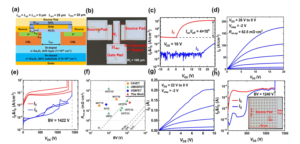
Figure 1 (a) Cross-sectional schematic of the fabricated β-Ga₂O₃ VDMOSFET; (b) Optical microscope image of the device; (c) Transfer characteristics; (d) Output characteristics; (e) Off-state breakdown characteristics; (f) Benchmark plot of Ron,sp and BV against state-of-the-art CBL-based vertical β-Ga₂O₃ MOSFETs; (g) Output curves of large-area array device; (h) Off-state breakdown curves of large-area device, inset shows optical image of transistor array
DOI:
doi.org/10.1007/s11432-025-4717-9
Instruction
Official Account

Cooperation
Top
