


Researchers from Nanjing University, Shantou University have published a dissertation titled "Valence-band engineering of robust p-type NiₓGa₁₋ₓO enabling Ga₂O₃ p-n bipolar junction" in Applied Physics Letters.
Background
β-Ga₂O₃ with an ultra-wide bandgap of 4.9 eV and theoretical breakdown field of 8 MV/cm is a promising candidate for next-generation high-power electronics. All existing Ga₂O₃ devices are unipolar devices, and the fabrication of high-performance bipolar devices is limited by the lack of reliable p-type doping. Conventional dopants such as N, Mg and Zn form deep acceptor levels, which suffer severe hole self-trapping and high hole effective mass, a common problem for wide-band oxides. Orbital hybridization can lift valence band maximum, but Bi/Ir doping suffers high cost and poor uniformity. NiO shows intrinsic p-type conduction and similar ionic radius with Ga³⁺, yet existing researches only characterize basic film properties. No systematic study on Ni composition modulation of band structure and transport behavior, and no high-breakdown Ga₂O₃ p-n power diodes have been demonstrated, forming a critical research gap for ultra-wide bandgap bipolar electronics.
Abstract
The absence of a reliable p-type ultrawide bandgap (UWBG) semiconductor remains a fundamental obstacle to the realization of bipolar Ga₂O₃-based power devices. Here, we demonstrate valence-band engineering in Ni-alloyed Ga₂O₃ (NiₓGa₁₋ₓO) to achieve robust p-type conduction. Strong Ni 3d-O 2p hybridization in NiₓGa₁₋ₓO effectively reshapes the valence band structures, elevating the valence band maximum and enabling hole transport for x>0.3. Increasing Ni composition from 0.32 to 0.62 in NiₓGa₁₋ₓO reduces the hopping activation energy to 0.06 eV, yielding a hole concentration of ~10¹⁸ cm⁻³ and resistivity near 40 Ω・cm while maintaining a wide bandgap of 4.5–4.1 eV. The constructed p-Ni0.62Ga0.38O /n-Ga₂O₃ diode exhibits distinct forward bipolar conduction modulation with rectification ratios >10¹⁰ at ±3 V, and a bilayer Ni0.32Ga0.68O / Ni0.62Ga0.38O structure enhances reverse blocking to 2.4 kV. These findings establish Ni-alloyed Ga₂O₃ as a robust p-type UWBG material for bipolar Ga₂O₃ power electronics.
Highlights
Realize valence band lifting via Ni 3d-O 2p orbital hybridization in NiₓGa₁₋ₓO alloy to achieve stable room-temperature p-type conduction for x > 0.3.
Reveal composition-dependent phase transition rule of NiₓGa₁₋ₓO and the corresponding hopping transport activation energy variation.
Fabricate single-layer p-Ni62Ga0.38O / n-Ga₂O₃diode with rectification ratio >10¹⁰ at ±3 V.
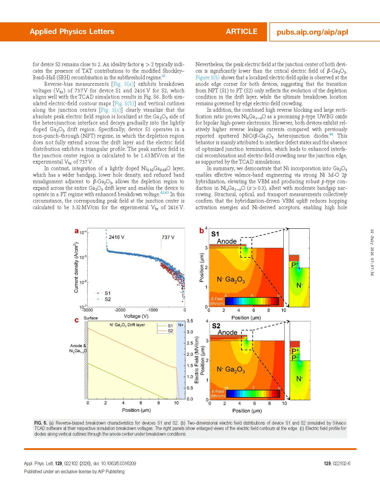
Propose bilayer graded p-type composite layer structure to redistribute junction electric field, boost breakdown voltage up to 2416 V.
Conclusion
In summary, we demonstrate that Ni incorporation into Ga₂O₃ enables effective valence-band engineering via strong Ni 3d–2p hybridization, elevating the VBM and producing robust p-type conduction in NiₓGa₁₋ₓO (x>0.3), albeit with moderate bandgap narrowing. Structural, optical, and transport measurements collectively confirm that the hybridization-driven VBM uplift reduces hopping activation energies and Ni-derived acceptors, enabling high hole concentration up to 10¹⁸ cm⁻³. Leveraging the electronic-structure modifications, p-Ni0.62Ga0.38O /n-Ga₂O₃ bipolar diodes exhibit bipolar forward conduction modulation with rectification ratios >10¹⁰, and a bilayer architecture further enhances reverse blocking capability up to 2.4 kV. These findings establish a ternary NiₓGa₁₋ₓO film as a promising platform for robust p-type conduction and a viable route toward bipolar Ga₂O₃ power electronics.
Project Support
This work was supported by the National Natural Science Foundation of China (Nos. 62234007, 62425403, 62293522, 623B2046, and 12374073), the Jiangsu Provincial Science and Technology Major Project (Nos. BG2024030 and BK20253003), the Guangdong Basic and Applied Basic Research Foundation (Nos. 2023A1515010556 and 2024A1515012961), Li Ka Shing Foundation (No. 2024LKSFG01), and the Postgraduate Research and Practice Innovation Program of Jiangsu Province (No. KYCX24_0142).
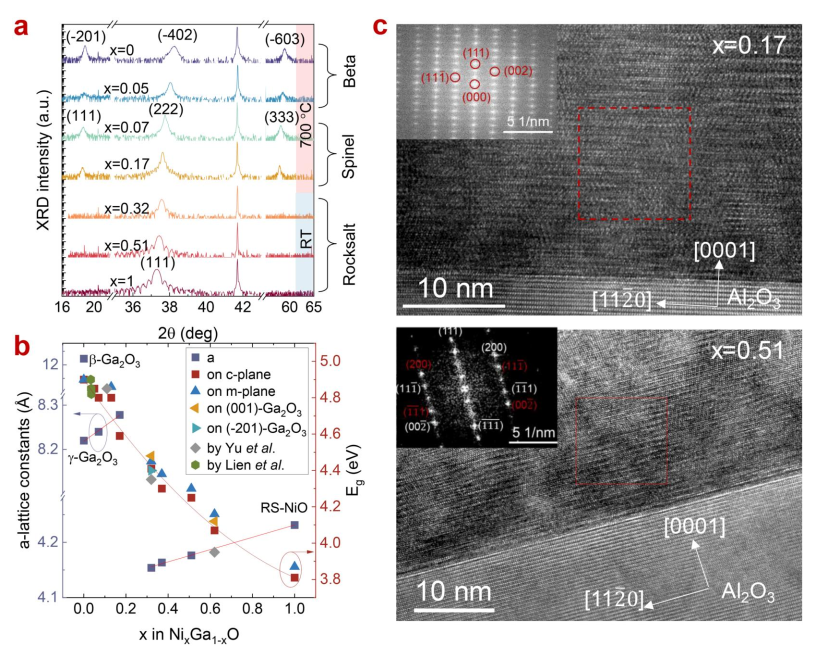
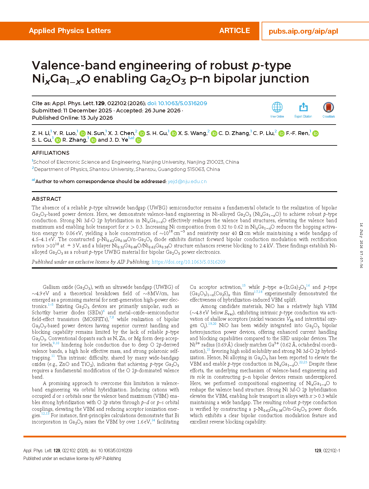
FIG. 1. (a) XRD patterns of NiₓGa₁₋ₓO films grown on c-plane sapphire. (b) Optical bandgap Eg and out-of-plane lattice constants of NiₓGa₁₋ₓO as a function of Ni composition (x). (c) Cross-sectional HRTEM images of NiₓGa₁₋ₓO with x=0.17 and x=0.51, and insets show the corresponding FFT patterns.
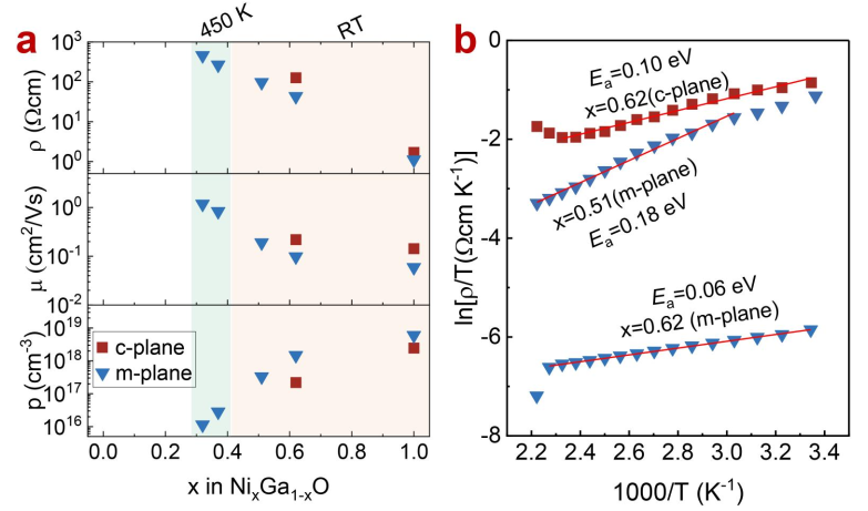
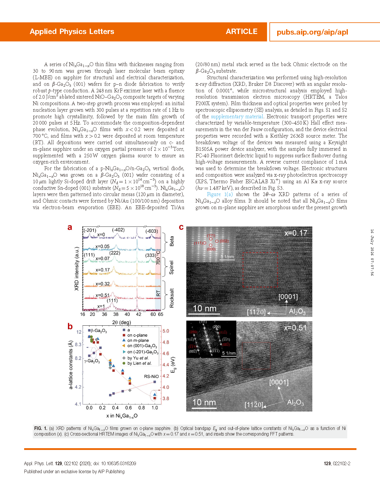
FIG. 2. (a) Resistivity, hole concentration, and mobility of NiₓGa₁₋ₓO films as a function of Ni composition x. Hall-effect measurement temperature regimes (450 K and RT) are marked. (b) Arrhenius plots of ln (ρ/T) vs 1/T for selected films, with linear fits shown as red lines.
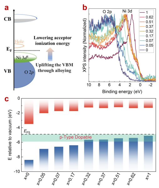
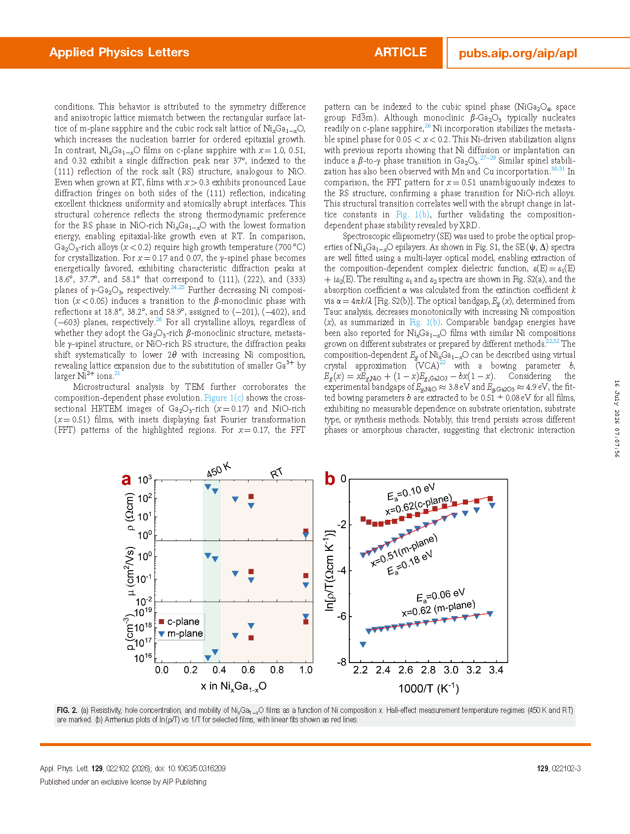
FIG. 3. (a) Schematic illustration of valence-band reconfiguration of NiₓGa₁₋ₓO. (b) Valence-band XPS spectra of Ga₂O₃, NiO, and NiₓGa₁₋ₓO with varying Ni composition. (c) VBM (EV) and CBM (EC) positions with respect to the vacuum level (Evac) of Ga₂O₃, NiO, and NiₓGa₁₋ₓO alloys.
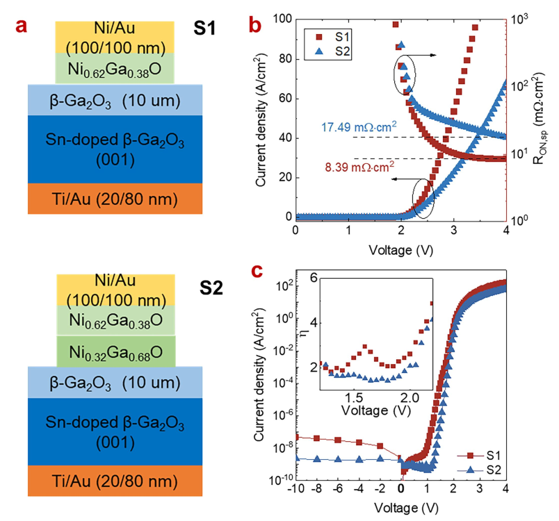
FIG. 4. (a) Cross-section schematics of vertical NiₓGa₁₋ₓO/Ga₂O₃ bipolar diodes. (b) Linear plots of J–V characteristics and extracted RON,sp as a function of forward bias. (c) Semi-logarithmic plots of J–V of NiₓGa₁₋ₓO/Ga₂O₃ bipolar diodes (S1 and S2), and extracted ideality factors as a function of forward bias (inset).
FIG. 5. (a) Reverse-biased breakdown characteristics for devices S1 and S2. (b) Two-dimensional electric field distributions of device S1 and S2 simulated by Silvaco TCAD software at their respective simulation breakdown voltages. The right panels show enlarged views of the electric field contours at the edge. (c) Electric field profile for diodes along vertical cutlines through the anode center under breakdown conditions.
DOI:
doi.org/10.1063/5.0316209

Instruction
Official Account

Cooperation
Top
