


The 19th National Conference on MOCVD will be held from July 27 to 29, 2026, in Hohhot, Inner Mongolia, China. The conference will focus on five major topics: “Material Growth, Characterization and Equipment,” “Power Electronics and RF Devices,” “Optoelectronic Devices and Applications,” “Ultra-Wide-Bandgap Semiconductors and Frontier Interdisciplinary Research,” and “Emerging Devices and New Applications for AI and Beyond.” The event aims to provide an important platform for in-depth academic discussions, technology exchange, and industry decision-making support.
Fujia Gallium has been invited to deliver a presentation at a dedicated session and will showcase multiple products and technologies at the exhibition.
Invited Presentation
Session 4: Ultra-Wide-Bandgap Semiconductors and Frontier Interdisciplinary Research
Speaker: Duanyang Chen, Deputy General Manager of Fujia Gallium
Presentation Title: MOCVD Homoepitaxy Technology and Industrialization Progress of Gallium Oxide
Time: July 29, 10:50–11:10 AM
Venue: Huamao Hotel, 4F Huajiu Hall
We sincerely welcome all attendees to join the session for on-site discussion and exchange.
Exhibition Highlights
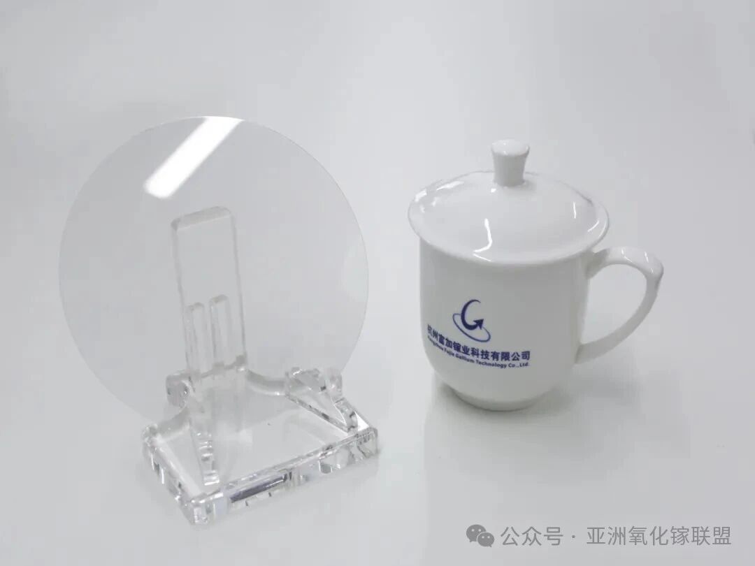
6/8-inch Gallium Oxide Substrates
Grown by Edge-defined Film-fed Growth (EFG) or Vertical Bridgman (VB) methods, the substrates are available in both semi-insulating and conductive types. They feature a double-crystal rocking curve full width at half maximum (FWHM) of ≤150″, a dislocation density of <1×10⁴ cm⁻², and surface roughness (Ra) of ≤0.5 nm.
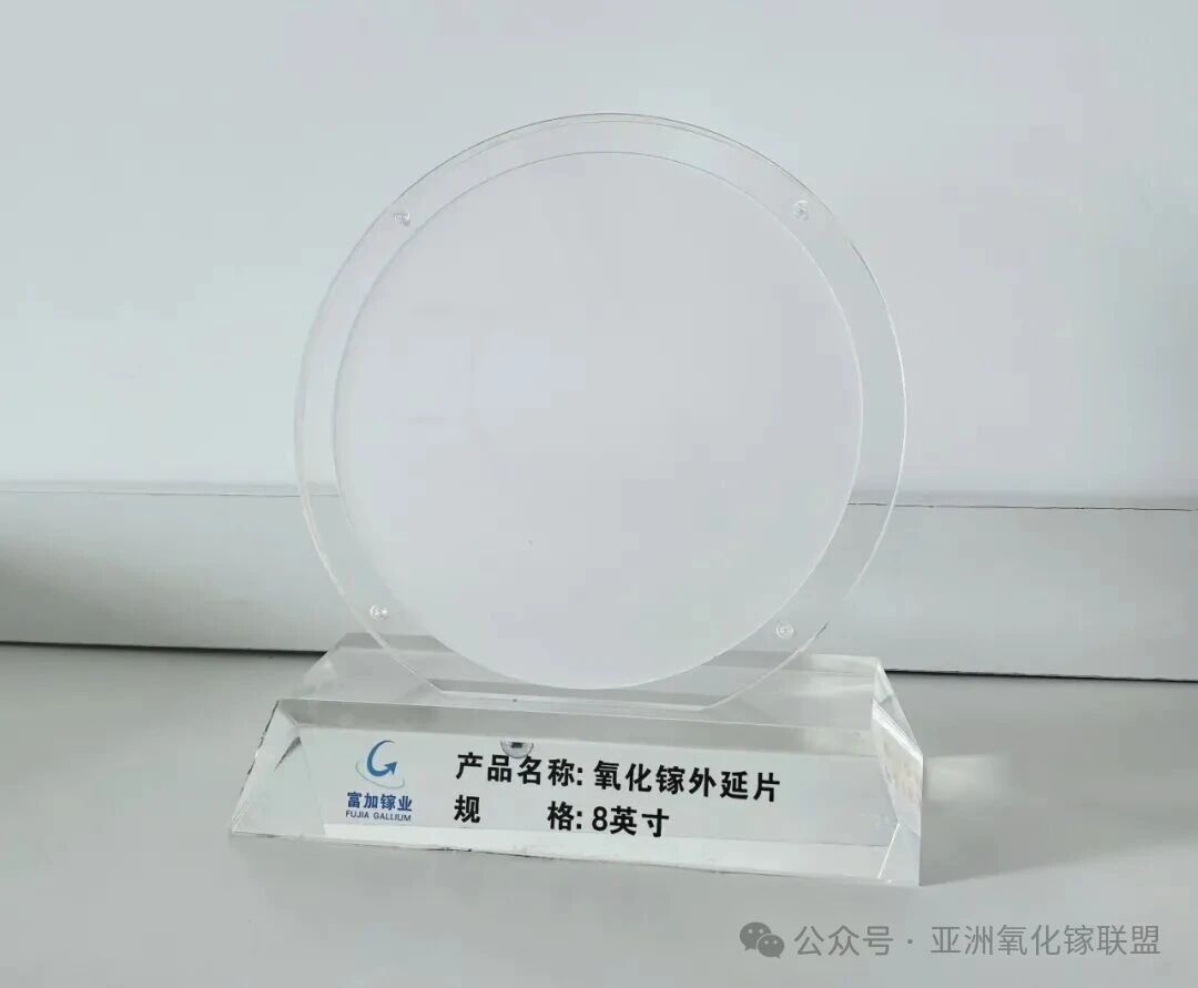
6/8-inch Gallium Oxide Homoepitaxial Wafers
Grown on conductive Ga₂O₃ substrates using metal-organic chemical vapor deposition (MOCVD) and molecular beam epitaxy (MBE) technologies, featuring an epitaxial layer thickness of >10 μm, a double-crystal rocking curve full width at half maximum (FWHM) ≤150″, and a surface roughness of Ra ≤5 nm.
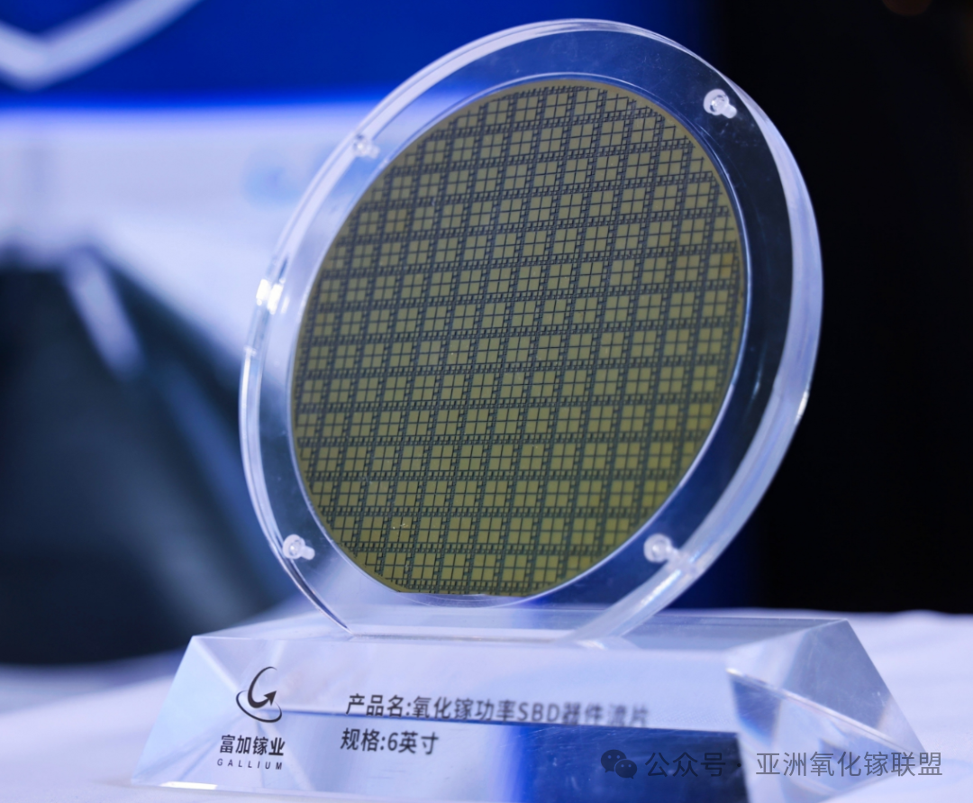
6-inch Gallium Oxide Power SBD Device Fabrication
Based on Fujia’s MOCVD homoepitaxial wafers, Fujia has completed the fabrication of kilovolt-ampere-class Ga₂O₃ SBD devices, achieving a breakdown voltage of >1200 V, a specific on-resistance of <20 mΩ·cm², and a forward current of >5 A at 3 V.
About Hangzhou Fujia Gallium
Hangzhou Fujia Gallium Technology Co., Ltd. was established on December 31, 2019. Guided by the vision of “Bringing Better Materials to the World,” the company is dedicated to the industrialization of ultra-wide-bandgap gallium oxide semiconductor materials. Its core products include gallium oxide single-crystal substrates, MOCVD/MBE epitaxial wafers, and crystal growth equipment based on the Vertical Bridgman (VB) and Edge-Defined Film-Fed Growth (EFG) methods. Recognized as a National High-Tech Enterprise, the company has undertaken multiple national and provincial/ministerial-level projects from the Ministry of Science and Technology, the National Development and Reform Commission, and the Ministry of Industry and Information Technology. It has been authorized nearly 70 international and domestic patents, and serves as the initiator and primary drafter of China's national standards in the field of gallium oxide. The company's series of major achievements in promoting gallium oxide industrialization have been featured in special coverages by prominent media outlets, including CCTV, People’s Daily, Xinhua News Agency, China Securities Journal, and The Paper.
Instruction
Official Account

Cooperation
Top
