


Researchers from Zhejiang University and Xidian University have published a dissertation titled " Carrier gas modulated surface dynamics and crystalline quality of (100) β-Ga₂O₃ homoepitaxial films via MOCVD " in Applied Surface Science.
Background
With an ultra-wide bandgap of ~4.9 eV, β-Ga₂O₃ exhibits an exceptionally high theoretical breakdown field strength of 8 MV/cm, which significantly surpasses traditional wide bandgap semiconductors such as SiC and GaN, making it an ideal material candidate for the fabrication of compact power electronic devices with high power density and low switching loss. Compared with other wide-bandgap materials, the melt method enables the cost-effective bulk growth of conductive and semi-insulating β-Ga₂O₃ single-crystal substrates with low dislocation density, which is a prerequisite for high-quality homoepitaxy and crucial for the economic feasibility of industrial applications.
Abstract
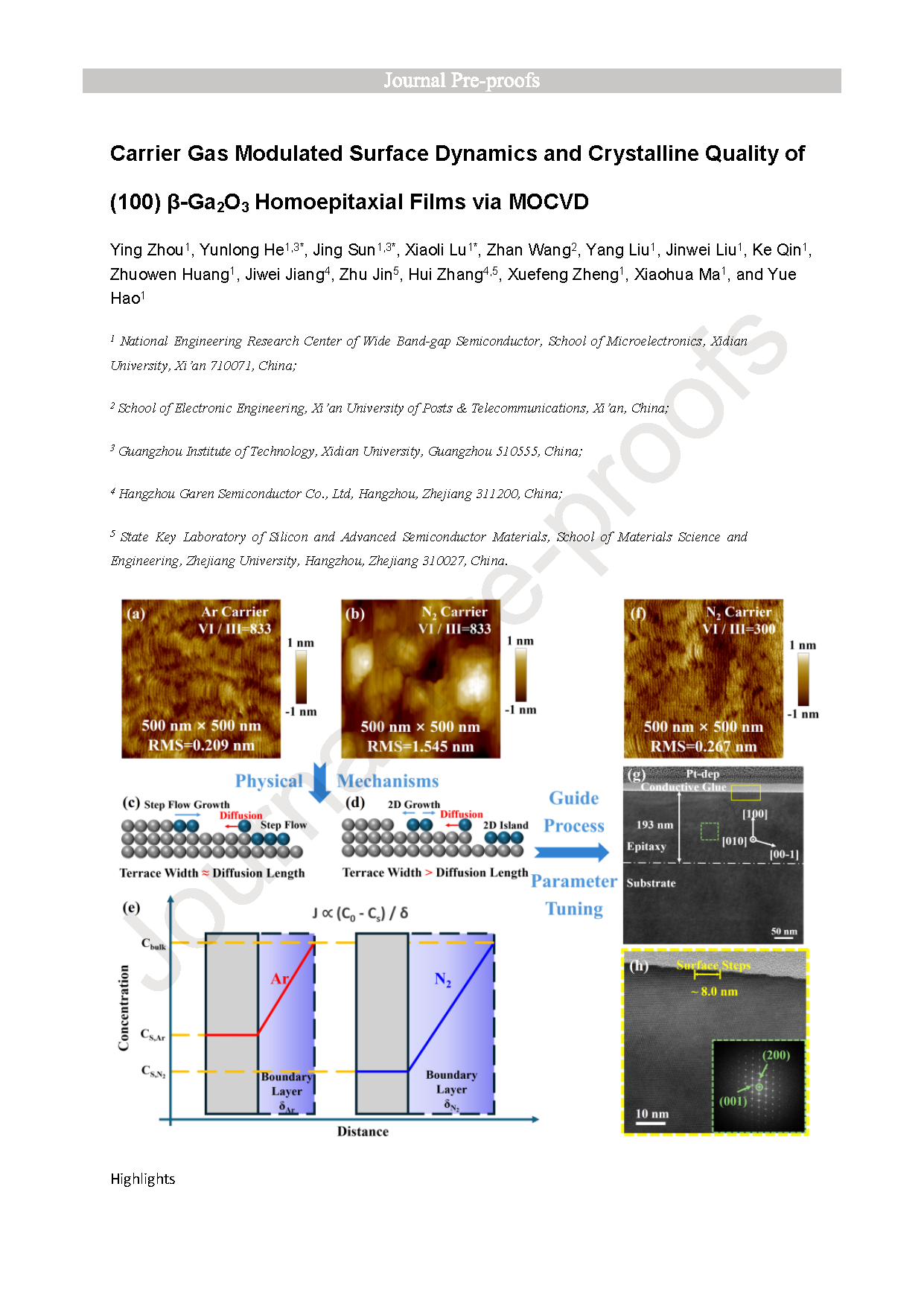
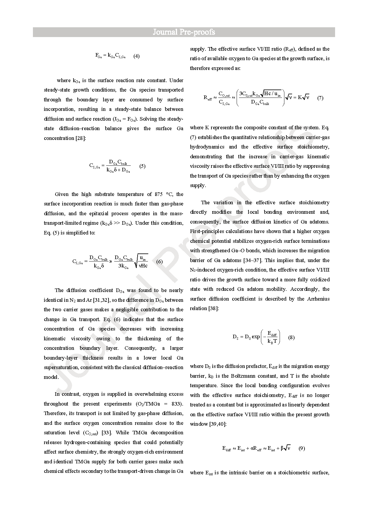
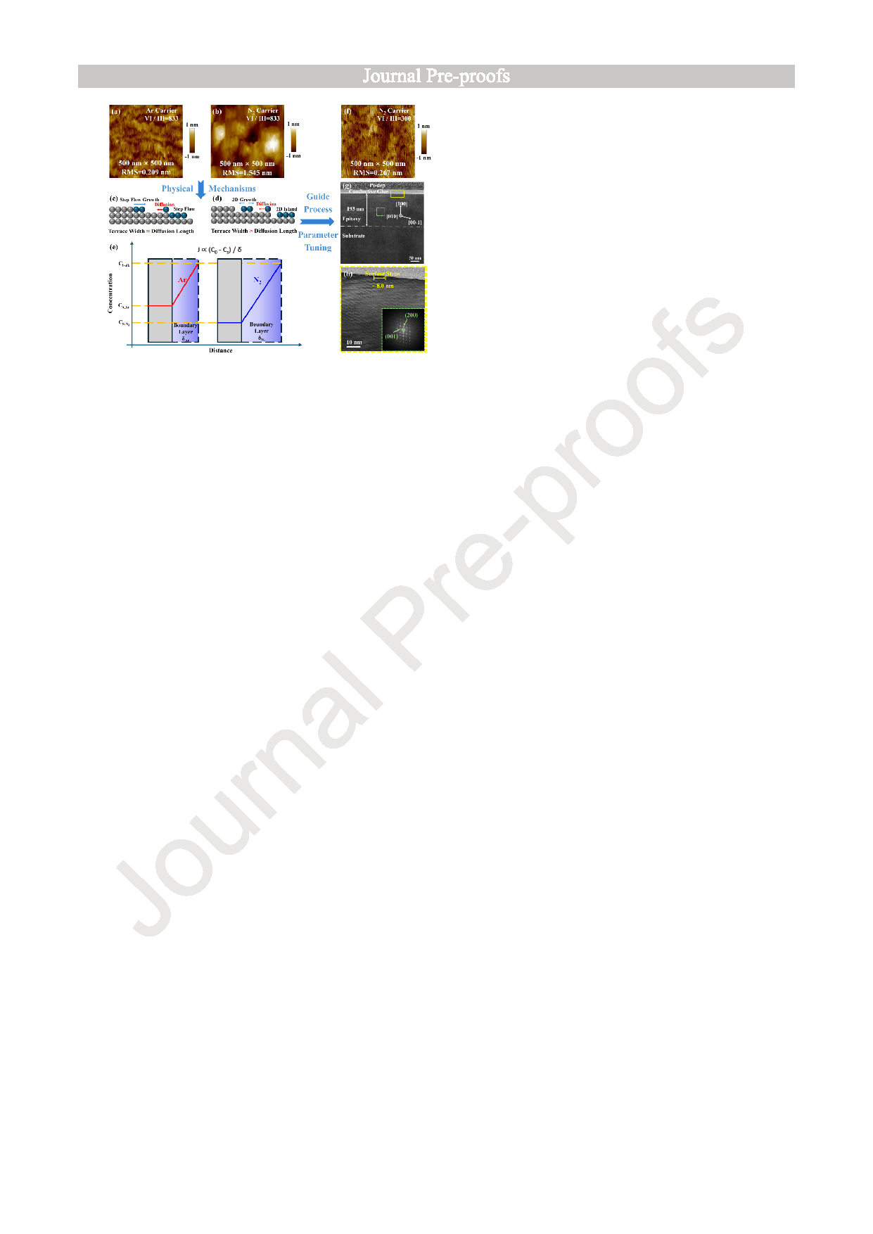
This study elucidates the physical mechanisms governing growth mode transitions in (100) β-Ga₂O₃ MOCVD homoepitaxy when replacing Ar with N₂ carrier gas. Ar promotes step-flow growth with RMS roughness of 0.209 nm and no twin defects. N₂ triggers 2D island nucleation, generating extensive twin boundaries and increasing roughness to 1.545 nm. Integrating boundary-layer mass-transfer kinetics with BCF theory, we find that the higher kinematic viscosity of N₂ forms a thicker boundary layer, impeding Ga precursor transport. This elevates the effective surface VI/III ratio, creating an oxygen-rich environment that increases the adatom migration barrier. Consequently, the Ga diffusion length drops below the critical terrace width, forcing the transition to 2D islanding. Guided by this framework, we optimized the N₂-driven process by tuning the O₂/TMGa molar flow ratio. At an optimal ratio of 300, the suppressed Ga diffusion kinetics are compensated, restoring step-flow growth. These optimized films show complete elimination of twin defects and a recovered RMS roughness of 0.267 nm. This work establishes a mechanistic framework linking carrier-gas properties to boundary-layer transport and surface diffusion kinetics, enabling rational process design for cost-effective scalable growth of device-grade β-Ga₂O₃ homoepitaxial films.
Conclusion
In summary, this study elucidated the pivotal role of carrier gas in governing the growth mode and crystalline integrity of (100) β-Ga₂O₃ homoepitaxial films via MOCVD. Under identical growth conditions, Ar promoted well-defined step-flow growth characterized by atomically smooth surfaces with an RMS roughness of 0.209 nm and a defect-free, highly ordered lattice. Conversely, N₂ induced 2D island growth that resulted in a substantially roughened surface with an RMS roughness of 1.545 nm, accompanied by an approximately 10 nm-thick interfacial defect region and high-density twin lamellae propagating throughout the epilayer. To realize controllable N₂-based growth, we established a unified theoretical framework by integrating the boundary-layer mass transfer model and classical BCF theory, unraveling the intrinsic mechanism. The higher kinematic viscosity of N₂ thickened the boundary layer and elevated the effective surface VI/III ratio, shortening Ga adatom diffusion length. When the adatom diffusion length fell below the substrate terrace width of 8 to 10 nm, 2D island growth was triggered. By optimizing the O₂/TMGa molar flow ratio to 300 to align the adatom diffusion length with the terrace width, high-quality step-flow growth with N₂ was achieved, restoring the surface RMS roughness to 0.267 nm and eliminating twin defects. The growth rate under this optimized condition is fully comparable to that of the standard Ar-based process. These findings clarified the fundamental interplay between carrier gas properties, boundary layer dynamics, and surface kinetics, thereby providing practical guidance for the cost-effective fabrication of high-performance β-Ga₂O₃ epitaxial films for power electronics.
Project Support
This work was supported by the National Natural Science Foundation of China (Grant Nos. 62474133, U2241220 and 10225417), the Guangdong Basic and Applied Basic Research Foundation (Grant No. 2025A1515011176), the Natural Science Basic Research Program of Shaanxi (Grant Nos. 2019JCW-14, 2020JCW-12), and the Fundamental Research Funds for the Central Universities (Grant No. YJSJ25013). (Corresponding author: Yunlong He, Jing Sun, Xiaoli Lu).
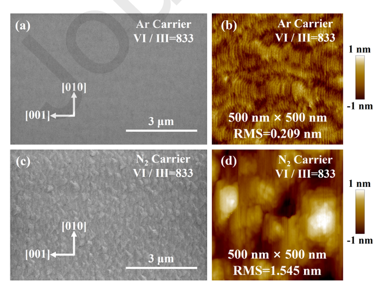
FIG.1 Surface morphology of (100) β-Ga₂O₃ films grown under different carrier gas conditions: (a) SEM and (b) AFM images of the film grown in Ar atmosphere with an O₂/TMGa molar flow ratio of 833; (c) SEM and (d) AFM images of the film grown in N₂ atmosphere with an O₂/TMGa molar flow ratio of 833. The corresponding growth conditions are summarized in Table I.
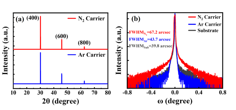
FIG.2 HRXRD characterization of (100) β-Ga₂O₃ films grown under different carrier gas conditions: (a) 2θ-ω scans; (b) Rocking curves of (400) plane for the films and the substrate.
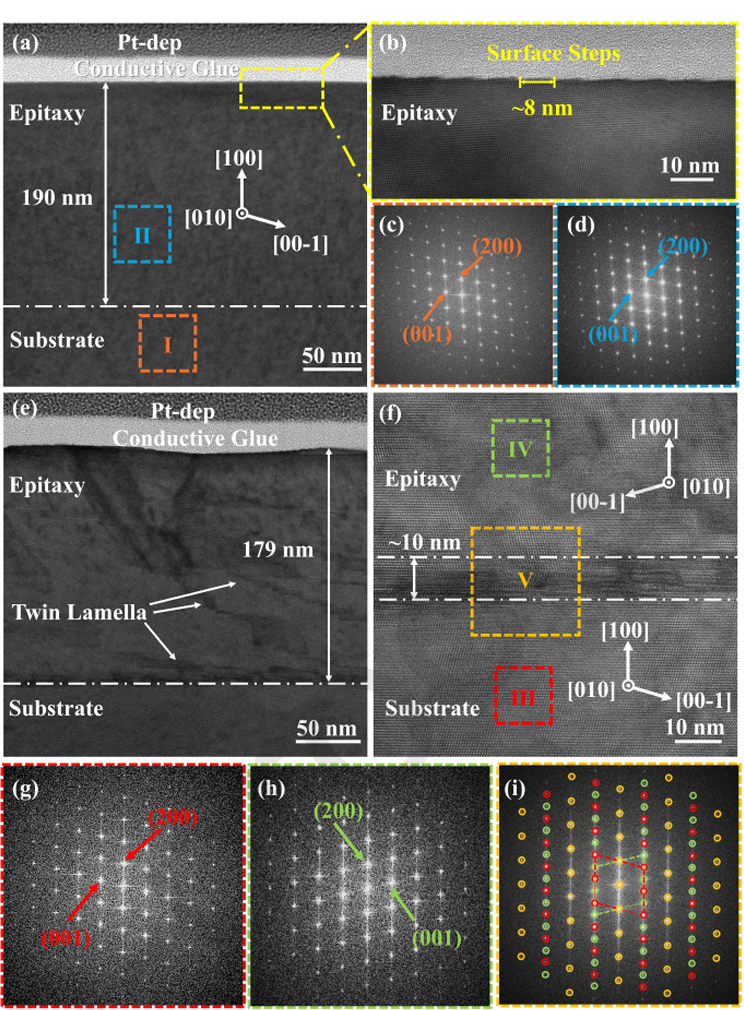
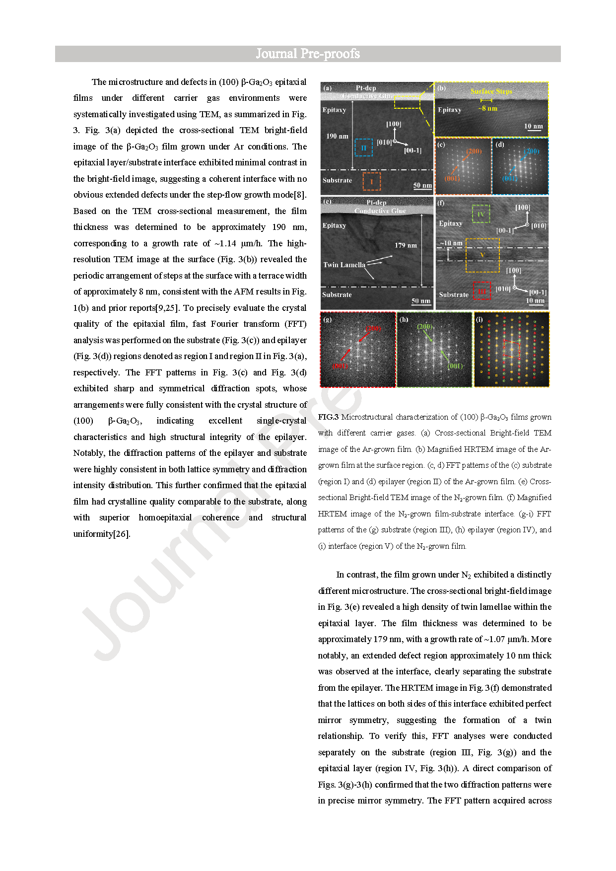
FIG.3 Microstructural characterization of (100) β-Ga₂O₃ films grown with different carrier gases. (a) Cross-sectional Bright-field TEM image of the Ar-grown film. (b) Magnified HRTEM image of the Ar grown film at the surface region. (c, d) FFT patterns of the (c) substrate (region I) and (d) epilayer (region II) of the Ar-grown film. (e) Cross sectional Bright-field TEM image of the N₂-grown film. (f) Magnified HRTEM image of the N₂-grown film-substrate interface. (g-i) FFT patterns of the (g) substrate (region III), (h) epilayer (region IV), and (i) interface (region V) of the N₂-grown film.
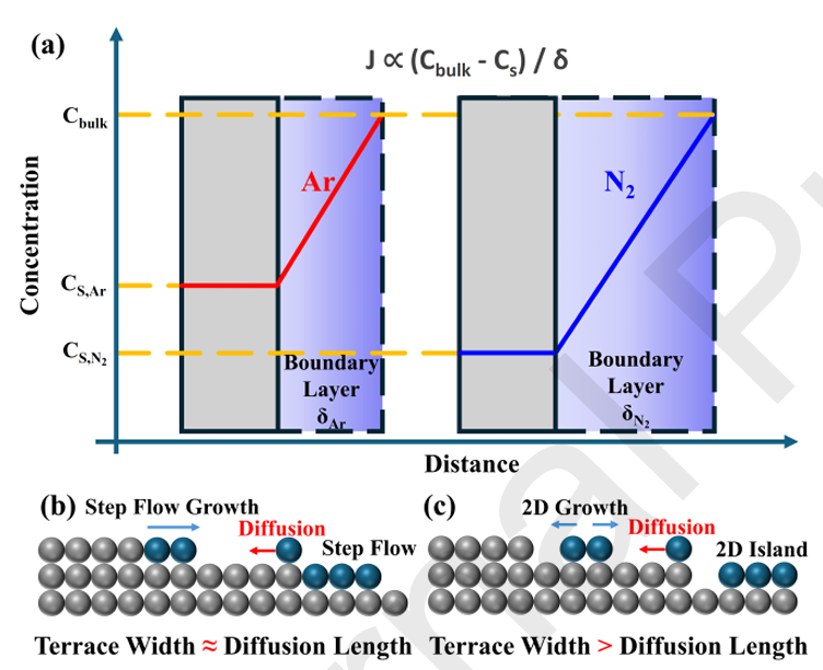
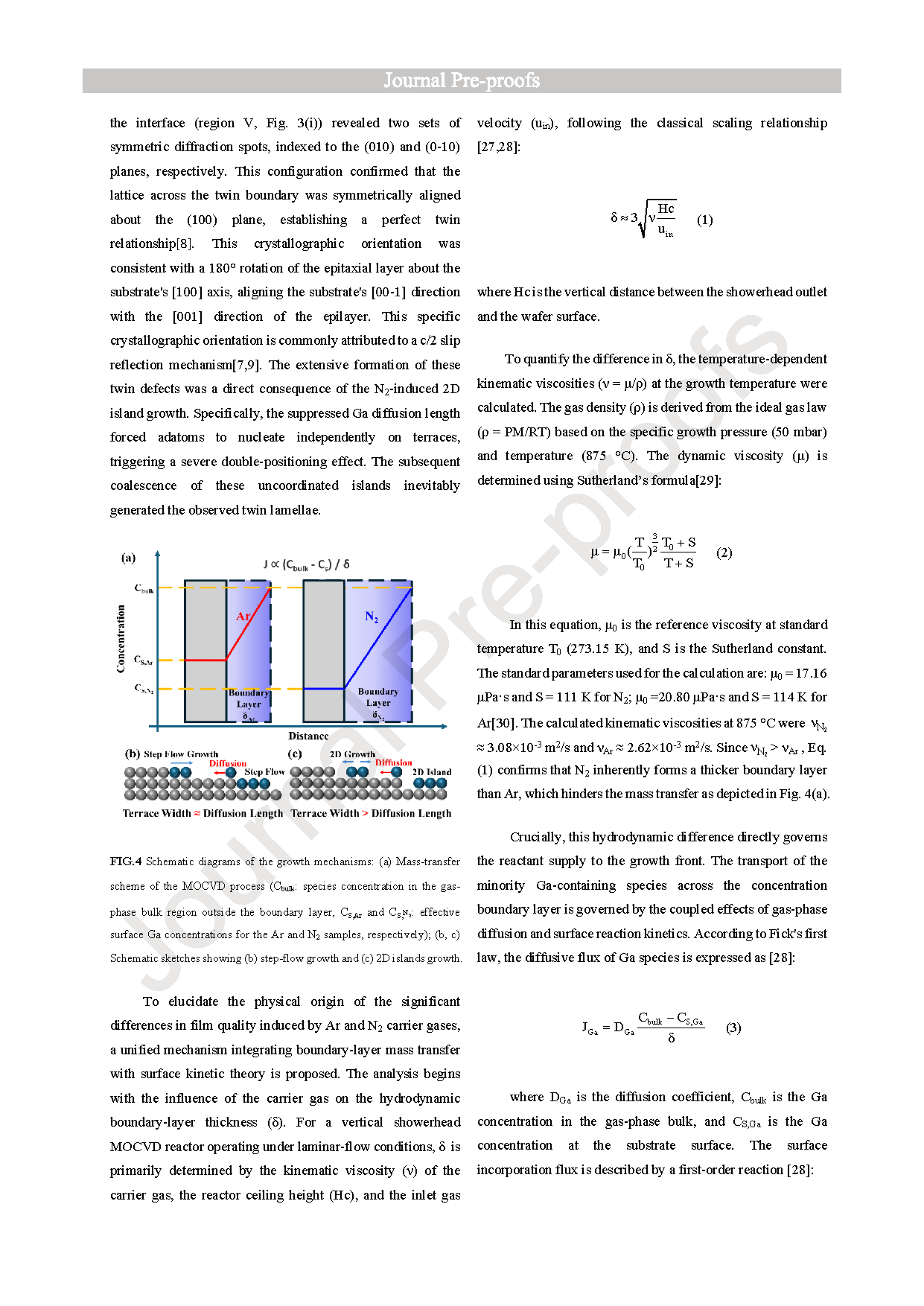
FIG.4 Schematic diagrams of the growth mechanisms: (a) Mass-transfer scheme of the MOCVD process (Cbulk: species concentration in the gas phase bulk region outside the boundary layer, CS,Ar and CS, N₂: effective surface Ga concentrations for the Ar and N₂ samples, respectively); (b, c) Schematic sketches showing (b) step-flow growth and (c) 2D islands growth.
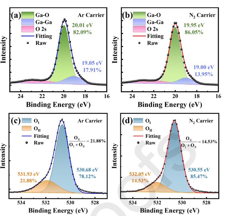
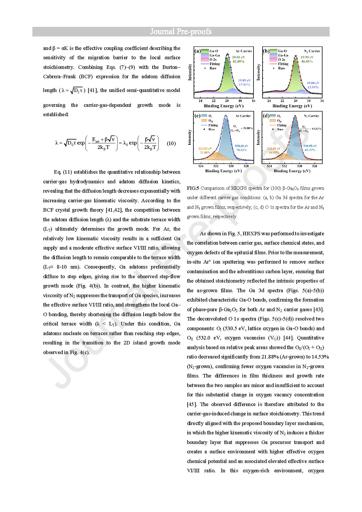
FIG.5 Comparison of HRXPS spectra for (100) β-Ga₂O₃ films grown under different carrier gas conditions: (a, b) Ga 3d spectra for the Ar and N₂ grown films, respectively; (c, d) O 1s spectra for the Ar and N₂ grown films, respectively.
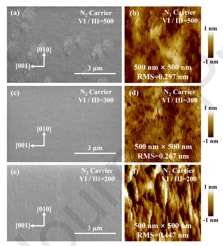
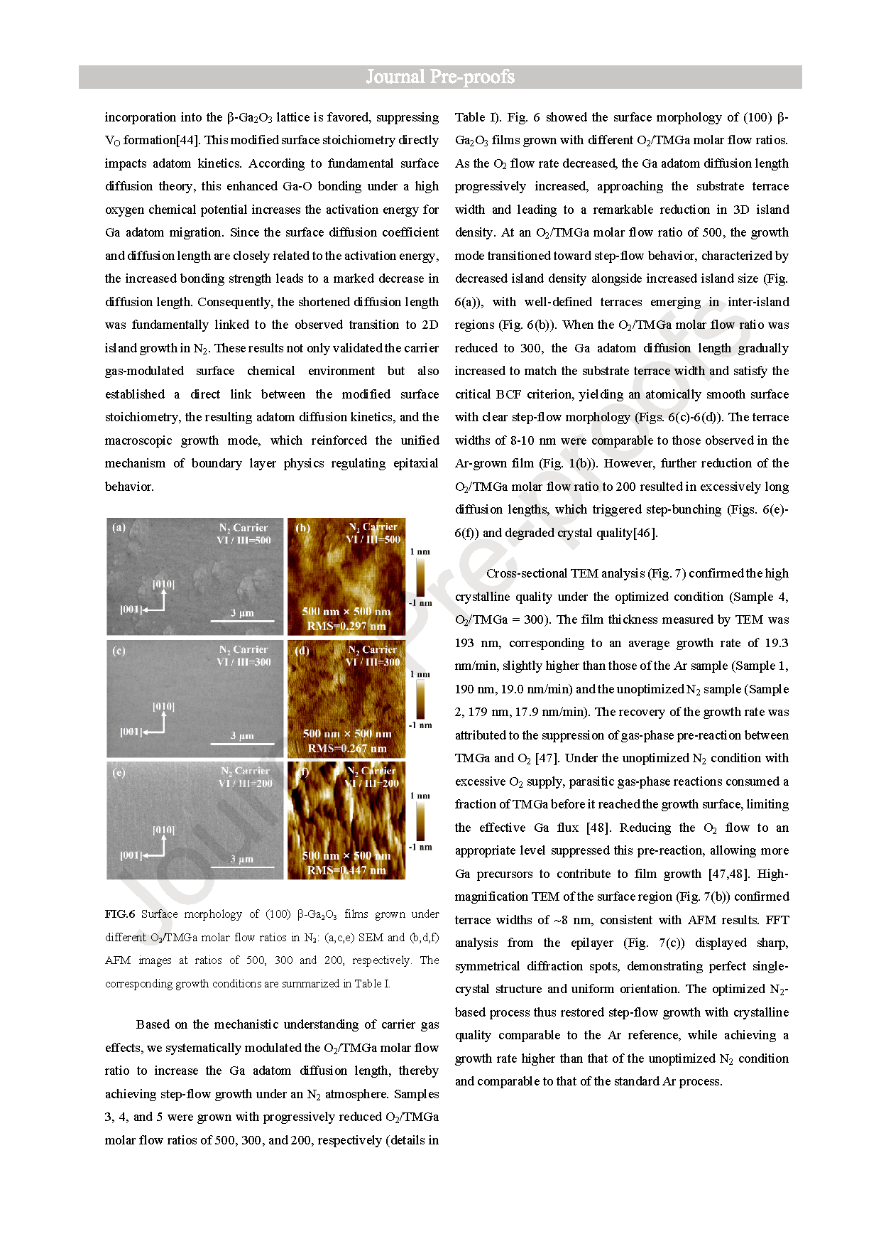
FIG.6 Surface morphology of (100) β-Ga₂O₃ films grown under different O₂/TMGa molar flow ratios in N₂: (a,c,e) SEM and (b,d,f) AFM images at ratios of 500, 300 and 200, respectively. The corresponding growth conditions are summarized in Table I.
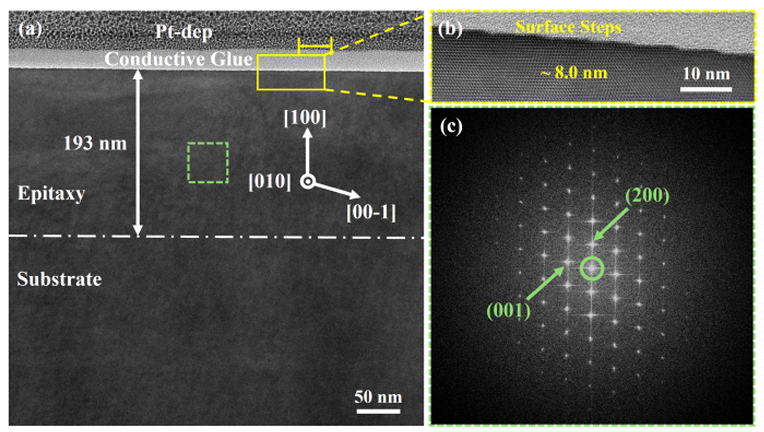
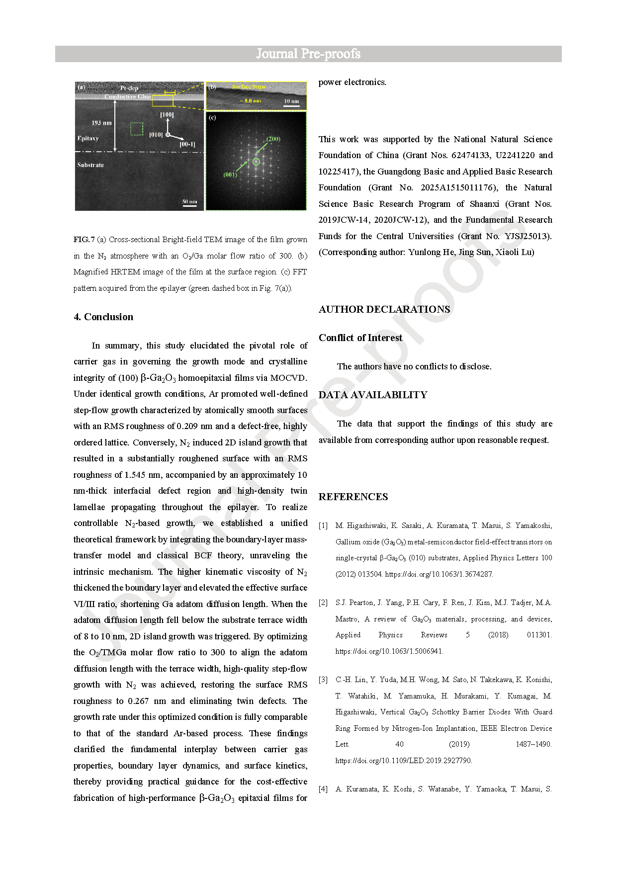
FIG.7 (a) Cross-sectional Bright-field TEM image of the film grown in the N₂ atmosphere with an O₂/Ga molar flow ratio of 300. (b) Magnified HRTEM image of the film at the surface region. (c) FFT pattern acquired from the epilayer (green dashed box in Fig. 7(a)).
DOI:
doi.org/10.1016/j.apsusc.2026.167950
Instruction
Official Account

Cooperation
Top
