


Recently, Hangzhou Fujia Gallium Technology Co., Ltd. has taken the lead in developing 12-inch gallium oxide MOCVD epitaxy technology, successfully extending its 8-inch gallium oxide MOCVD epitaxial process to 12-inch wafers for the first time.
Key Metrics: Uniform Thickness and High-Quality Epitaxial Films
The 12-inch Ga₂O₃ epitaxial film developed based on the 8-inch MOCVD epitaxial process demonstrates excellent thickness uniformity of better than 6%. After epitaxial growth, the as-grown surface maintains a high degree of flatness, marking a significant step forward toward the industrialization of large-size Ga₂O₃ MOCVD epitaxy technology.
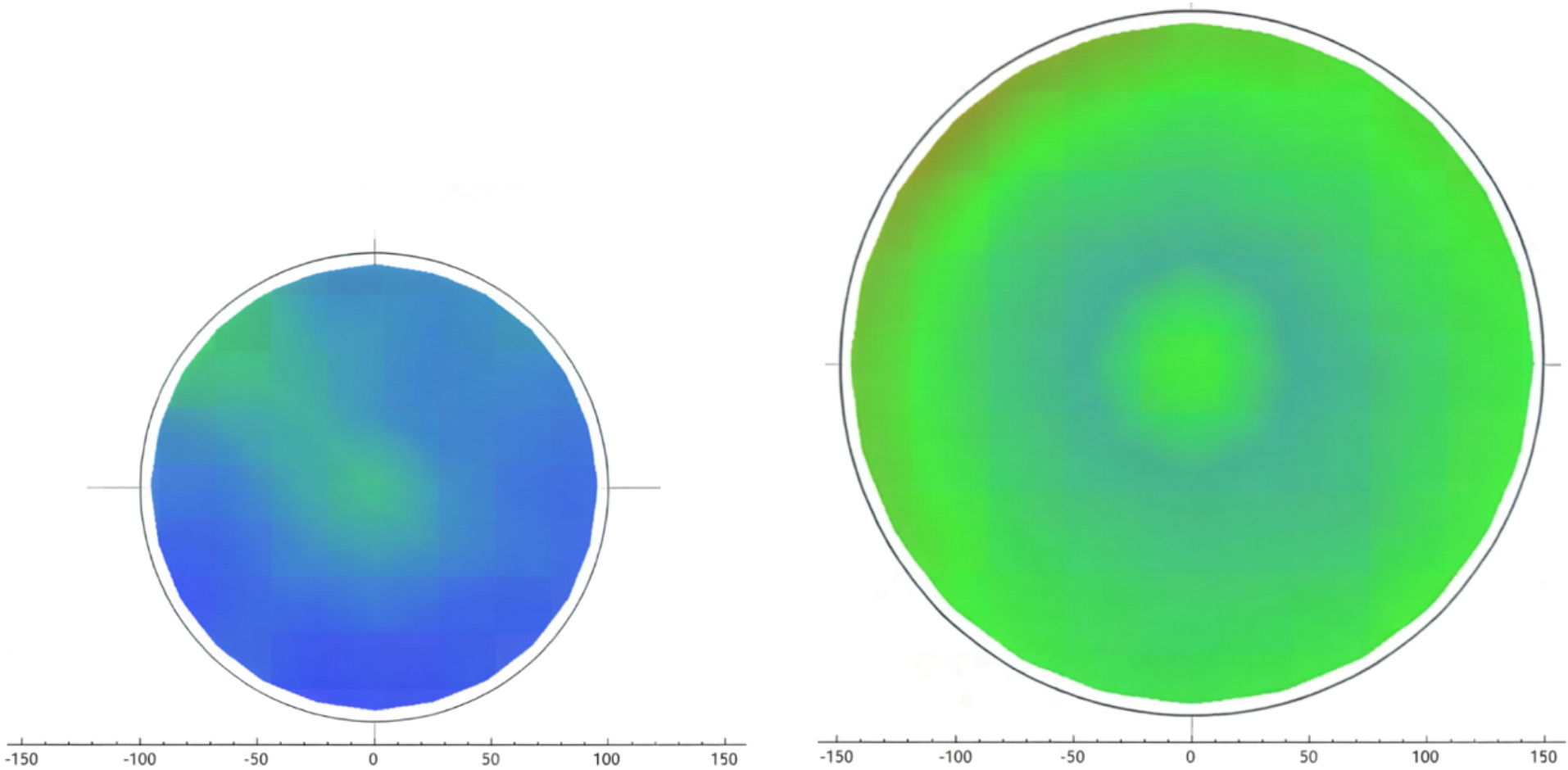
▲ Comparison of Epitaxial Thickness Distribution Between 8-inch (left) and 12-inch (right) Ga₂O₃ Wafers
Fujia Gallium successfully fabricated 10 μm-thick 8-inch homoepitaxial Ga₂O₃ wafers in March 2026, achieving a thickness uniformity better than 3%, a surface roughness (RMS) below 1 nm, and an X-ray diffraction (XRD) rocking curve full width at half maximum (FWHM) of only 64.8 arcsec. The epitaxial wafers are directly applicable for power device fabrication.
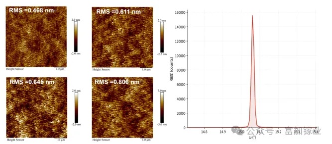
▲ Surface roughness (AFM) and X-ray rocking curve (FWHM = 64.8 arcsec) of the 8-inch Ga₂O₃ homoepitaxial wafer
From 8-inch to 12-inch: Accelerating the Industrialization Process
The theoretical number of devices obtainable from a 12-inch epitaxial wafer is approximately 2.25 times that of an 8-inch wafer. The development of large-size epitaxial wafers will significantly reduce the manufacturing cost of Ga₂O₃ devices and accelerate their transition from laboratory research to industrial-scale production.
Combined with its mass-produced 6-inch and 8-inch substrates and the world’s first released 12-inch Ga₂O₃ single crystal, Fujia Gallium is building a comprehensive Ga₂O₃ material supply chain covering “equipment–substrate–epitaxy”, providing downstream device manufacturers with integrated material solutions.
Fujia Gallium will continue to uphold its mission of “Bringing Better Materials to the World”, driving the ultra-wide-bandgap semiconductor industry toward a broader future through higher-quality products.
About Hangzhou Fujia Gallium
Hangzhou Fujia Gallium Technology Co., Ltd. was established on December 31, 2019. Guided by the vision of “Bringing Better Materials to the World,” the company is dedicated to the industrialization of ultra-wide-bandgap gallium oxide semiconductor materials. Its core products include gallium oxide single-crystal substrates, MOCVD/MBE epitaxial wafers, and crystal growth equipment based on the Vertical Bridgman (VB) and Edge-Defined Film-Fed Growth (EFG) methods. Recognized as a National High-Tech Enterprise, the company has undertaken multiple national and provincial/ministerial-level projects from the Ministry of Science and Technology, the National Development and Reform Commission, and the Ministry of Industry and Information Technology. It has been authorized nearly 70 international and domestic patents, and serves as the initiator and primary drafter of China's national standards in the field of gallium oxide. The company's series of major achievements in promoting gallium oxide industrialization have been featured in special coverages by prominent media outlets, including CCTV, People’s Daily, Xinhua News Agency, China Securities Journal, and The Paper.
Instruction
Official Account

Cooperation
Top
