


Researchers from the Pusan National University and Dong-Eui University and University of Oslo have published a dissertation titled "Compensation-Controlled Adaptive Transport and High-Voltage Operation in β-Ga₂O₃ Single Crystals" in Materials Today Physics.
Background
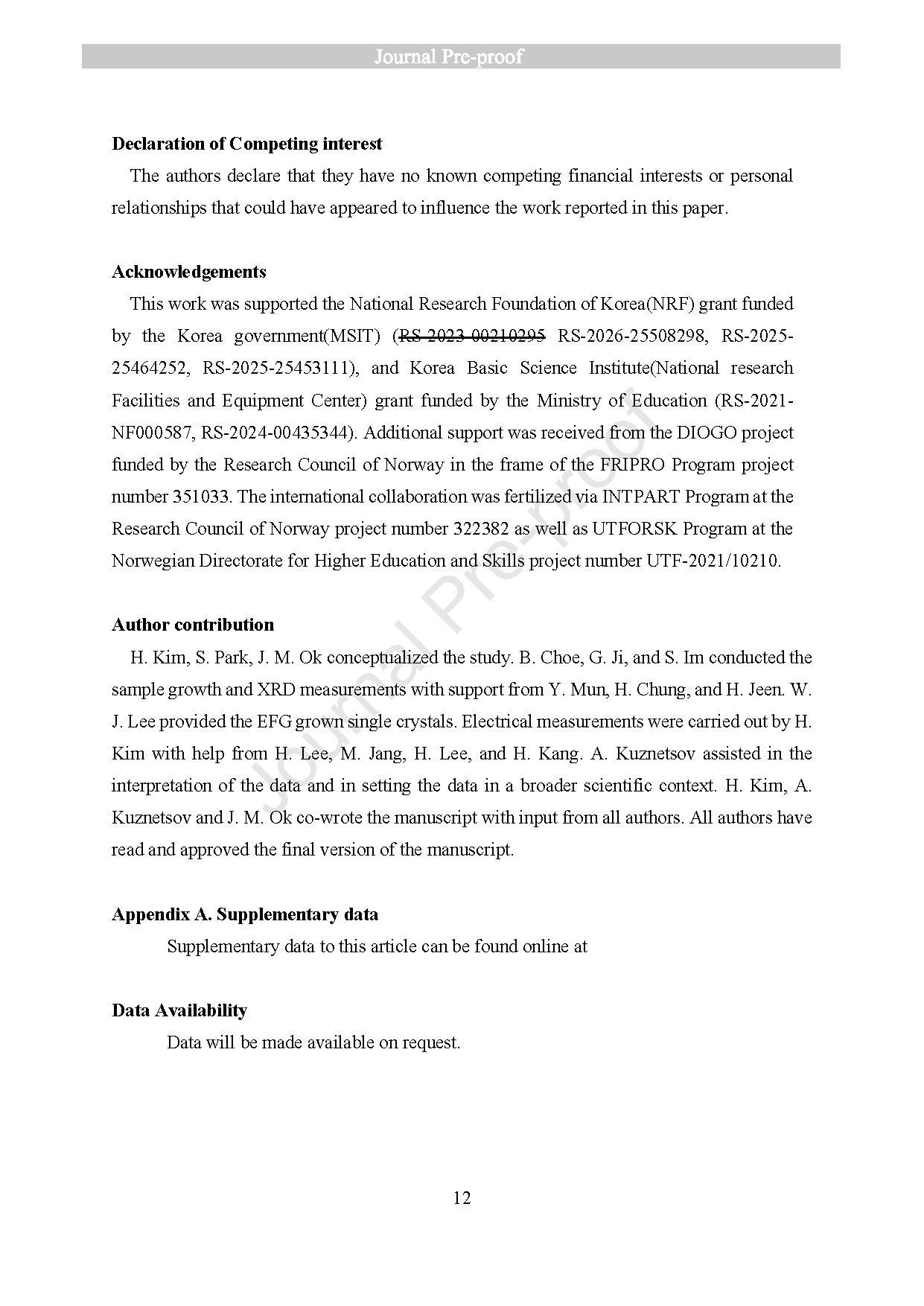
For aerospace, deep space exploration and defense electronics working under extreme environments, semiconductors are required to operate stably from cryogenic to high temperatures. However, conventional semiconductors suffer inherent limitations in temperature adaptability. Narrow-bandgap semiconductors such as SiGe and GaAs can retain conductivity at low temperatures but suffer excessive leakage current and poor thermal stability under high temperature. Wide-bandgap materials including SiC and GaN exhibit outstanding high-temperature endurance, yet severe carrier freeze-out occurs at cryogenic temperatures, leading to drastically increased device resistance. Extraterrestrial environments like the Moon and Mercury feature extreme temperature fluctuations; single-type semiconductor devices cannot cover the full temperature window, requiring multiple discrete device platforms and raising system complexity and reliability risks.
Defect-mediated hopping transport has been proposed as a candidate to eliminate low-temperature carrier freeze-out, where localized in-gap states provide conductive pathways when thermally activated carriers vanish. Nevertheless, an inherent trade-off exists in defect density: insufficient localized states fail to sustain cryogenic conduction, while excessive defects degrade breakdown voltage and high-voltage performance of power devices.
The donor-acceptor compensation ratio defined as K=NA/ND acts as a central parameter governing defect network distribution. Prior works have not systematically revealed the coupling between compensation level, temperature-dependent evolution of transport mechanisms, and high-voltage performance of Schottky diodes. Besides, systematic experimental verification of magnetic-field response under strong carrier localization is still lacking. In this work, β-Ga₂O₃ single-crystal Schottky diodes are investigated. Single crystals with low and high compensation ratios are fabricated by tuning oxygen partial pressure during crystal growth, establishing a comprehensive framework of compensation engineering to control adaptive full-temperature transport and high-voltage device behaviors.
Abstract
Reliable semiconductor operation across cryogenic to high temperatures remains a fundamental challenge for space and defense electronics, as wide-bandgap semiconductors suffer from carrier freeze-out at low temperatures while narrow-bandgap systems degrade at elevated temperatures. Here, we demonstrate stable rectifying operation in β-Ga₂O₃ Schottky diodes and compensation-dependent transport evolution in β-Ga₂O₃ single crystals over a wide temperature range. Low-compensation single-crystal devices exhibit a crossover from band conduction to hopping transport while sustaining conduction down to cryogenic temperatures, and maintaining a high breakdown voltage of ~3000 V, far exceeding the few-hundred-volt range typically reported for single-crystal β-Ga₂O₃ Schottky diodes. In contrast, higher-compensation samples exhibit more temperature-stable transport but lower breakdown voltages, indicating that high-voltage behavior is strongly affected by the compensation-related defect landscape together with carrier concentration and impurity/defect density. Within the low-compensation regime, we further identify Efros-Shklovskii variable-range hopping conduction under strong localization, which is highly sensitive to magnetic fields and leads to field-induced current suppression via enhanced localization. These results establish donor-acceptor compensation as a key parameter for controlling transport-regime evolution, while showing that high-voltage operation requires simultaneous consideration of compensation, carrier concentration, and impurity/defect control, thereby providing a pathway toward robust semiconductor operation under extreme temperature and field conditions.
Highlights
①Donor-acceptor compensation engineering enables adaptive sequential transport transitions in β-Ga₂O₃ from band conduction to NNH, Mott VRH and ES VRH across cryogenic to high temperatures.
②Low-compensation β-Ga₂O₃ single-crystal Schottky diodes achieve an ultrahigh breakdown voltage of ~3000 V, overcoming the conventional trade-off between cryogenic conductivity and high-voltage performance.
③Distinct magnetic-field-sensitive transport behavior is discovered in the Efros-Shklovskii variable-range hopping regime; external magnetic fields above critical field Hc≈4 T suppress carrier hopping via enhanced localization.
④A quantitative compensation map in NA-ND space is established to correlate defect landscape, Fermi level position and temperature-dependent diode characteristics.
Conclusion
In this study, we demonstrate that donor-acceptor compensation serves as a unifying control parameter that governs both charge transport and high-voltage device performance in β-Ga₂O₃ across a wide temperature range. By systematically tuning the compensation ratio, we reveal that transport does not remain fixed to a single mechanism but instead evolves sequentially from band conduction to NNH, Mott VRH, and ES VRH as temperature decreases. We show that low-compensation crystals enable this adaptive transport evolution while simultaneously achieving an exceptionally high breakdown voltage of ~3000 V, highlighting a unique regime where both cryogenic conduction and high-field stability are realized. In contrast, higher-compensation samples maintain continuous conduction via defect-mediated pathways but suffer from reduced breakdown performance associated with a higher defect population, establishing a clear trade-off governed by compensation. Importantly, in the ES VRH regime, we uncover a magnetic-field-responsive transport behavior arising from enhanced localization, where conduction is suppressed beyond a critical field due to the competition between hopping length rhop and magnetic confinement. This behavior introduces a new functionality in which carrier transport can be actively modulated by external magnetic fields. These findings establish compensation engineering as a key strategy for designing ultrawide-bandgap semiconductor devices with self-adaptive conduction and high-voltage and field-responsive operation, with potential relevance to cryogenic electronics, high-power devices, and extreme-environment applications.
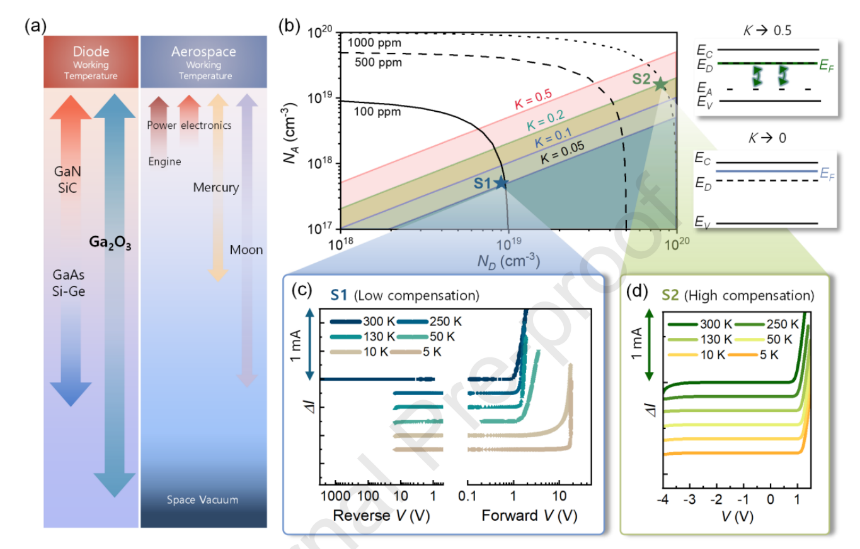
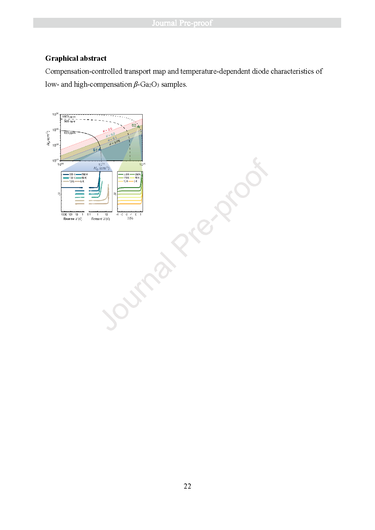
Fig. 1. Compensation-dependent transport window and Schottky diode characteristics of β-Ga₂O₃ single crystals across cryogenic and high-temperature regimes. (a) Comparison of the operating temperature ranges of representative semiconductor Schottky diodes with those relevant to aeronautical and space environments. In contrast to conventional narrow- and wide-bandgap semiconductors, β-Ga₂O₃ exhibits an exceptionally broad operating window. The right panel indicates representative temperature ranges for aircraft systems, power electronics, the Moon, Mercury, and space vacuum. (b) Schematic transport map in the NA-ND parameter space, where the total impurity concentration is defined as NA+ND and the compensation ratio as K=NA/ND. Colored lines represent constant compensation ratios (K=0.5, 0.2, 0.1, and 0.05), with shaded regions shown for visual guidance. Black dashed lines denote constant total impurity concentrations (1000, 500, and 100 ppm). Star symbols mark the approximate locations of S1 and S2. The right upper and right lower insets illustrate the limiting band alignments for K→0.5 and K→0, respectively. (c) Temperature-dependent reverse- and forward-bias I-V characteristics of the low-compensation sample S1, showing stable reverse-blocking behavior and preserved diode turn-on behavior down to low temperature. (d) Temperature-dependent I-V characteristics of the higher compensation sample S2, showing more continuous low-temperature transport but reduced reverse breakdown voltage.
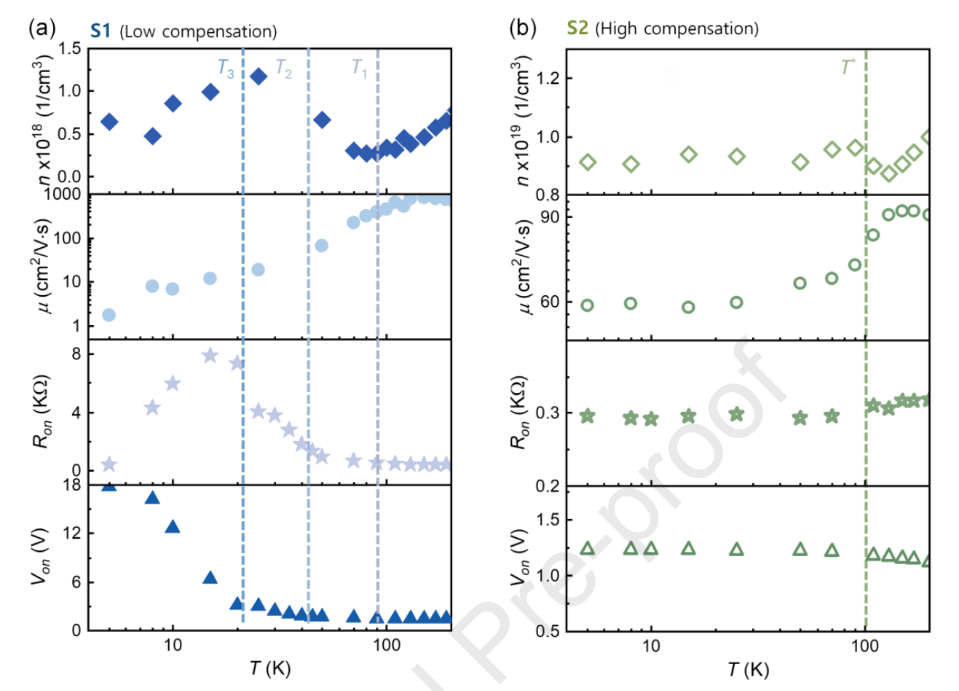
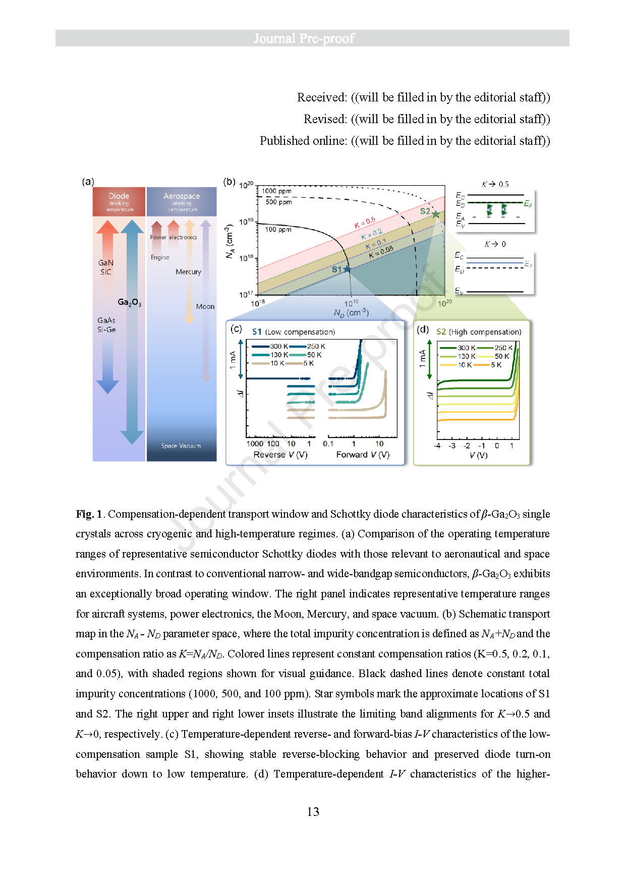
Fig. 2. Hall and diode measurements reveal β-Ga₂O₃ charge transport over a wide temperature range. Temperature-dependent evolution of four key transport parameters: carrier concentration n (diamonds) and mobility μ (circles) extracted from Hall measurements, and Ron (stars) and Von (triangles) obtained from diode characteristics. (a) S1 sample showing sequential changes in transport behavior across T1, T2, and T3. Three characteristic transition temperatures (T1≈80 K, T2≈40 K, and T3≈15 K), marked by vertical dotted lines, indicate successive changes in the dominant conduction mechanism. (b) S2 sample exhibiting relatively weak temperature dependence of all transport parameters, indicating more continuous defect-mediated transport with only weak crossover signatures and without the pronounced sequential transitions observed in S1.
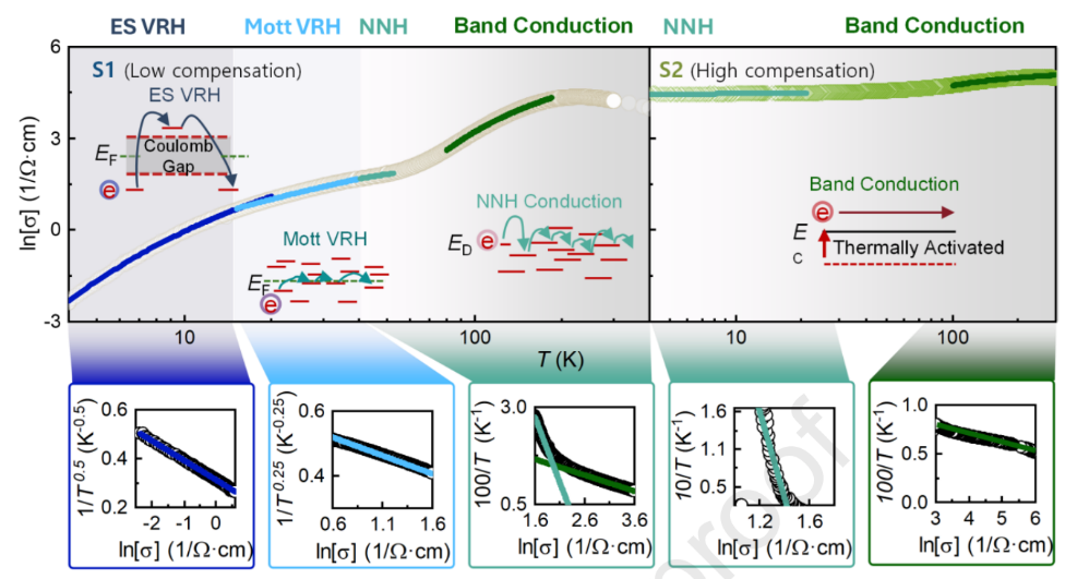
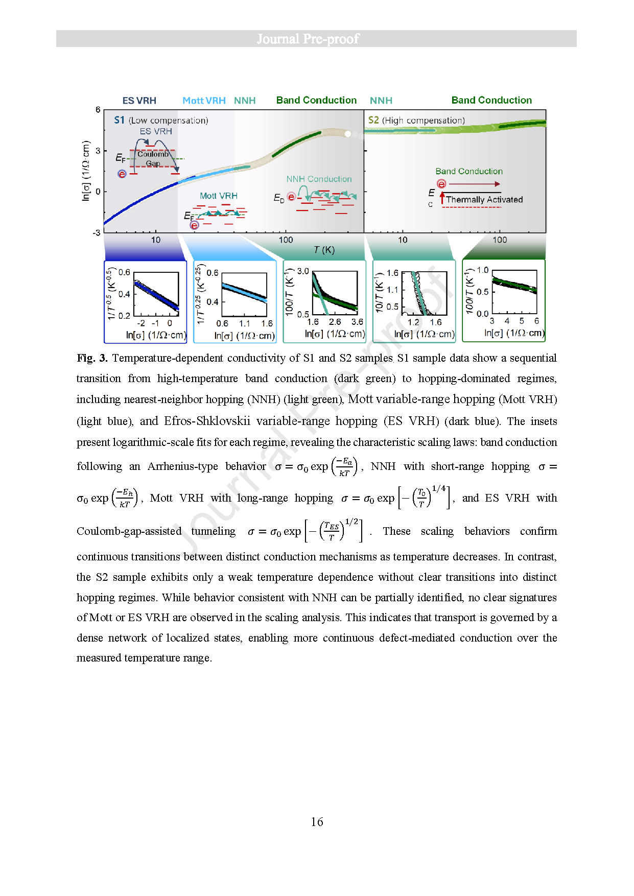
Fig. 3. Temperature-dependent conductivity of S1 and S2 samples. S1 sample data show a sequential transition from high-temperature band conduction (dark green) to hopping-dominated regimes, including nearest-neighbor hopping (NNH) (light green), Mott variable-range hopping (Mott VRH) (light blue), and Efros-Shklovskii variable-range hopping (ES VRH) (dark blue). The insets present logarithmic-scale fits for each regime, revealing the characteristic scaling laws: band conduction following an Arrhenius-type behavior σ=σ0 exp (-Ea/kT), NNH with short-range hopping σ=σ0 exp (-Eh/kT), Mott VRH with long-range hopping σ=σ0 exp [-(T0/T)^1/4], and ES VRH with Coulomb-gap-assisted tunneling σ=σ0 exp [-(TES/T)^1/2]. These scaling behaviors confirm continuous transitions between distinct conduction mechanisms as temperature decreases. In contrast, the S2 sample exhibits only a weak temperature dependence without clear transitions into distinct hopping regimes. While behavior consistent with NNH can be partially identified, no clear signatures of Mott or ES VRH are observed in the scaling analysis. This indicates that transport is governed by a dense network of localized states, enabling more continuous defect-mediated conduction over the measured temperature range.
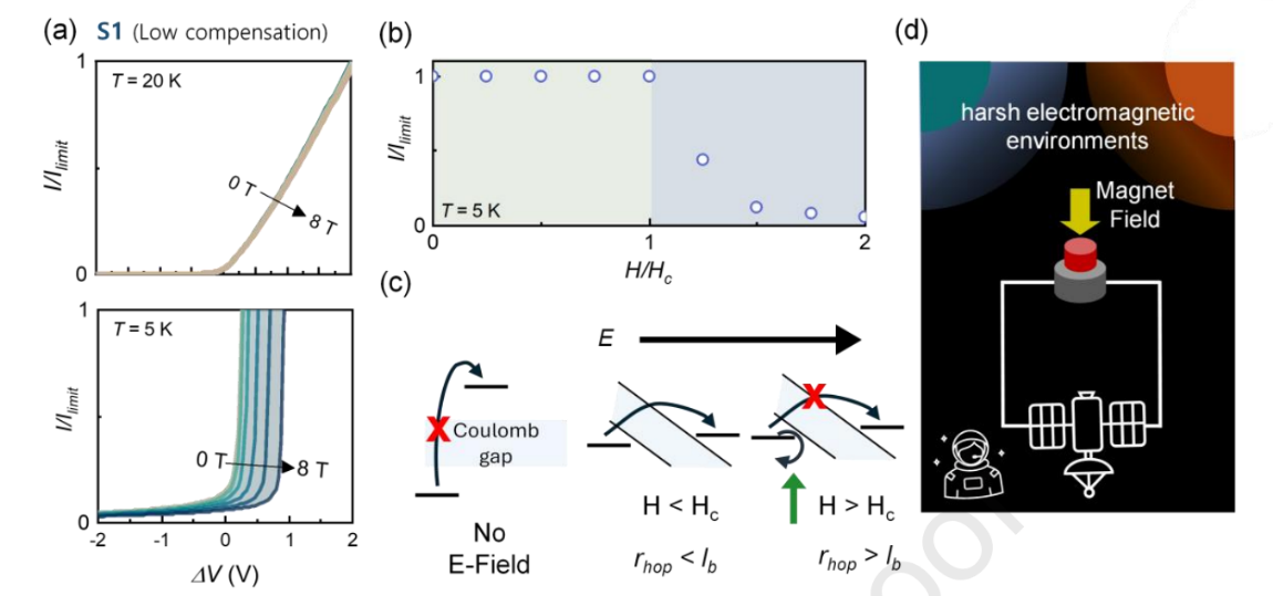
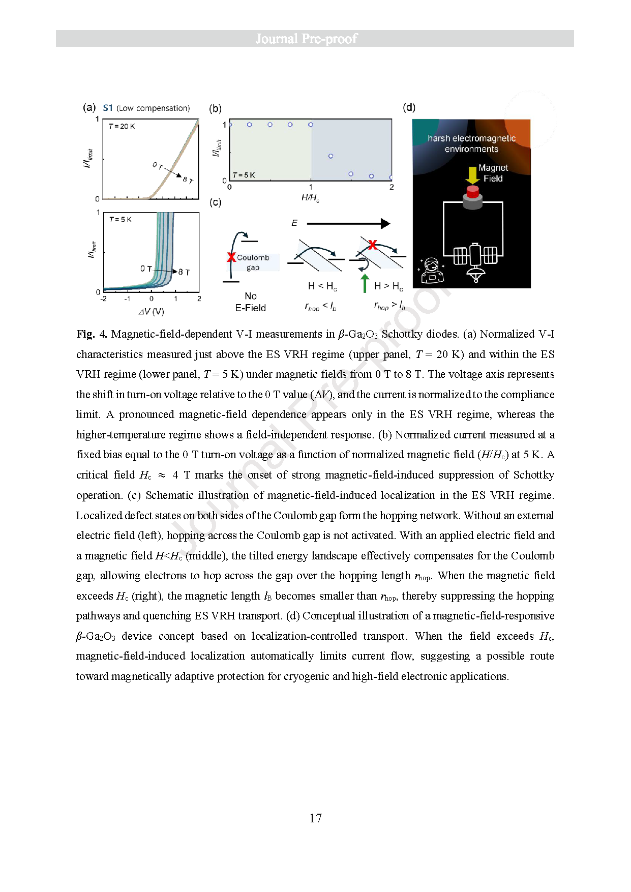
Fig. 4. Magnetic-field-dependent V-I measurements in β-Ga₂O₃ Schottky diodes. (a) Normalized V-I characteristics measured just above the ES VRH regime (upper panel, T=20 K) and within the ES VRH regime (lower panel, T=5 K) under magnetic fields from 0 T to 8 T. The voltage axis represents the shift in turn-on voltage relative to the 0 T value (ΔV), and the current is normalized to the compliance limit. A pronounced magnetic-field dependence appears only in the ES VRH regime, whereas the higher-temperature regime shows a field-independent response. (b) Normalized current measured at a fixed bias equal to the 0 T turn-on voltage as a function of normalized magnetic field (H/Hc) at 5 K. A critical field Hc≈4 T marks the onset of strong magnetic-field-induced suppression of Schottky operation. (c) Schematic illustration of magnetic-field-induced localization in the ES VRH regime. Localized defect states on both sides of the Coulomb gap form the hopping network. Without an external electric field (left), hopping across the Coulomb gap is not activated. With an applied electric field and a magnetic field H<Hc (middle), the tilted energy landscape effectively compensates for the Coulomb gap, allowing electrons to hop across the gap over the hopping length rhop. When the magnetic field exceeds Hc (right), the magnetic length lB becomes smaller than rhop, thereby suppressing the hopping pathways and quenching ES VRH transport. (d) Conceptual illustration of a magnetic-field-responsive β-Ga₂O₃ device concept based on localization-controlled transport. When the field exceeds Hc, magnetic-field-induced localization automatically limits current flow, suggesting a possible route toward magnetically adaptive protection for cryogenic and high-field electronic applications.
DOI :
doi.org/10.1016/j.mtphys.2026.102170
Instruction
Official Account

Cooperation
Top
