


Researchers from the University of Science and Technology of China and National University of Singapore have published a dissertation titled "0.79 mΩ·cm2 and 1.1 kV Vertical Mo/β-Ga2O3 Deep-Trench-HJBS Diode with Double Drift Layers " in 2026 IEEE 38th International Symposium on Power Semiconductor Devices and ICs.
Background
The advancement of wide-bandgap semiconductors and related power electronics technologies brings tremendous transformative potential to the entire energy industry for realizing carbon neutrality. As core devices for high-efficiency electric energy conversion, power diodes play a vital role in reducing energy loss and improving the overall efficiency of power systems. Beta-phase gallium oxide (β-Ga₂O₃), an ultra-wide bandgap material, has a bandgap of approximately 4.8 eV, a critical electric field up to 8 MV/cm, and its theoretical Baliga’s figure of merit is about 3444 times that of silicon. In addition, high-quality melt-grown single crystal substrates of β-Ga₂O₃ can be produced in large scale at low cost, which provides key support for developing high-voltage power devices with low power loss.
Reduced surface field (RESURF) technology has been widely applied in high-voltage SiC power devices to mitigate the trade-off between turn-on voltage and reverse leakage current, yet its bipolar implementation faces huge challenges in β-Ga₂O₃ due to the absence of intrinsic bipolar doping. Recently, p-type nickel oxide (p-NiO) with a bandgap of 3.4~4 eV has been adopted to construct heterojunction structures for β-Ga₂O₃ diodes. Heterojunction barrier Schottky (HJBS) diodes with alternating p-n junctions can achieve favorable forward conduction and suppressed reverse leakage current. Embedding p-NiO into n-type β-Ga₂O₃ trenches generates stronger lateral depletion compared with surface p-type layers, which more effectively suppresses reverse leakage current.
Two critical contradictions restrict the development of low-loss high-voltage β-Ga₂O₃ power diodes. First, low-barrier conductive channels for reducing turn-on voltage will trigger severe reverse leakage current under high reverse electric fields owing to the image-force-induced barrier lowering effect. Second, thinning epitaxial layers or increasing doping concentration to cut specific on-resistance will sacrifice the voltage sustaining region and degrade breakdown voltage. Conventional shallow-trench β-Ga₂O₃ devices have limited sidewall conduction area, resulting in insufficient optimization of conduction loss. There is a lack of integrated structural design combining double drift layers, deep trenches and sidewall-embedded p-NiO to simultaneously realize kV-class breakdown voltage, ultra-low specific on-resistance and ultra-low reverse leakage current. Therefore, this paper proposes a novel deep-trench HJBS diode with double drift layers to resolve the inherent trade-off.
Abstract
This work demonstrates a vertical β-Ga₂O₃ deep-trench heterojunction barrier Schottky (DT-HJBS) diode with double drift layers. A low work-function metal Mo anode is employed to achieve a low turn-on voltage (Von), while sputtered p-NiO integrated on the trench sidewalls effectively suppresses the reverse leakage current (JR). By employing a double drift layer, the device achieves a favorable compromise between breakdown voltage (Vbr) and specific on-resistance (Ron,sp), leading to an enhanced power figure-of-merit (PFOM). Moreover, by increasing the trench depth and narrowing the fin width to achieve higher fin density, the sidewall conduction area is expanded, thereby further reducing the Ron,sp. Ultimately, the DT-HJBS diode exhibits an ultra-low Ron,sp of 0.79 mΩ·cm², an ultra-low JR<1 μA/cm² at -1000 V, a Vbr of 1088V and a high PFOM of 1.5 GW/cm², showing significant potential in high-performance power diode applications.
Highlights
A vertical Mo/β-Ga₂O₃deep-trench heterojunction barrier Schottky (DT-HJBS) diode with double drift layers is proposed. The thin lightly doped top drift layer and thick heavily doped bottom drift layer jointly balance breakdown voltage and specific on-resistance, and improve the power figure-of-merit (PFOM).
Synergistic design of metal anode and heterojunction: Low-work-function Mo metal is adopted as Schottky anode to reduce turn-on voltage (Von). Sputtered p-NiO conformal coating on trench sidewalls generates lateral depletion of p-n heterojunction to drastically suppress reverse leakage current (JR), breaking the inherent trade-off between low Vonand low JR.
Optimized trench fabrication process: The ICP-RIE dry etching recipe is optimized to minimize sidewall surface roughness and realize uniform continuous conformal coverage of p-NiO on trench sidewalls. Increasing trench depth and reducing fin width raise fin density, expand sidewall conductive area and further cut Ron,sp.
Record comprehensive electrical performance: The fabricated diode achieves ultra-low Ron,sp of 0.79 mΩ·cm², ultra-low JR < 1 μA/cm² under -1000 V, kV-class Vbr of 1088 V and high PFOM of 1.5 GW/cm², outperforming previously reported vertical β-Ga₂O₃ diodes.
Conclusion
In summary, we demonstrated a vertical Mo/β-Ga₂O₃ DT-HJBS diode with a double drift layer. The bilayer epitaxial structure design effectively reduces the Ron,sp of the device while also accommodating the enhancement of voltage withstand capability. The low qΦB Schottky junction formed by the low-work-function metal Mo lowers the Von of the device. Meanwhile, in combination with the lateral depletion effect generated by the sidewall-embedded p-NiO layer, it effectively suppresses the JR from the Schottky active region. Furthermore, by increasing the trench depth and reducing the fin width, the effective conductive area of the sidewalls is enlarged, leading to a further reduction in Ron,sp. Finally, ultra-low Ron,sp of 0.79 mΩ·cm², a low leakage current density (<1 μA/cm²) at -1000V, a kV-Class Vbr of 1088 V, and a Von of 1.04 V were simultaneously achieved in the DT-HJBS diode. These results demonstrate the promising potential of β-Ga₂O₃ power devices for high-voltage applications with low conduction loss.
Project Support
This work was supported by the National Natural Science Foundation of China under Grant Nos. 62234007, U23A20358, 62522411, 62404214, and 62474170, the National Key Research and Development Program of China (No. 2024YFE0205200), Provincial Science and Technology Major Project of Jiangsu under Grant No. BG2024030.
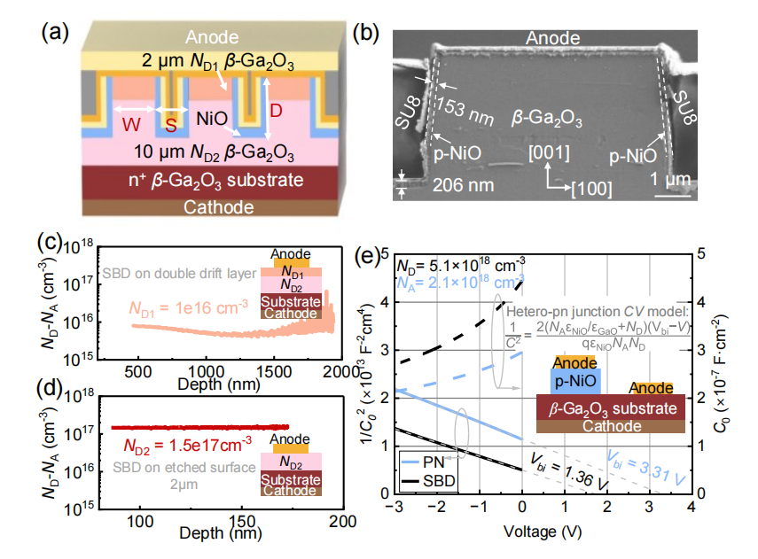
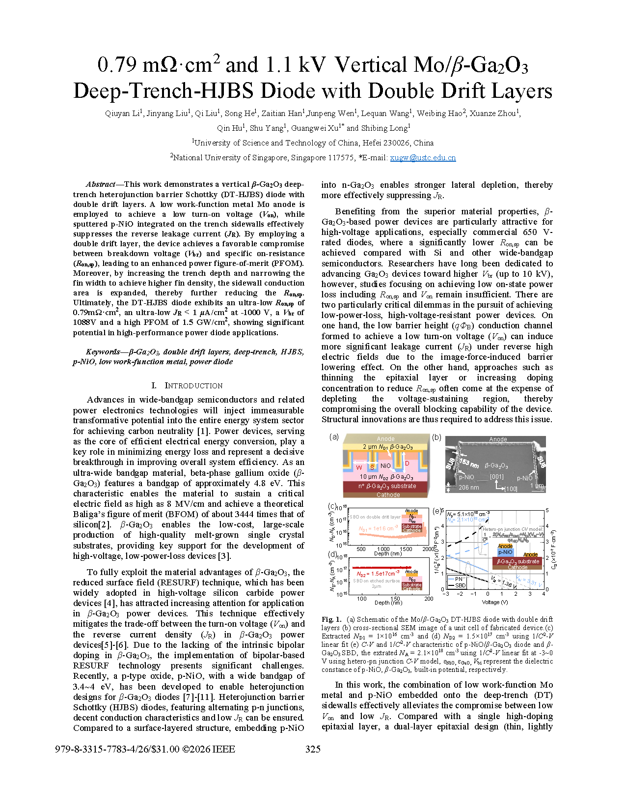
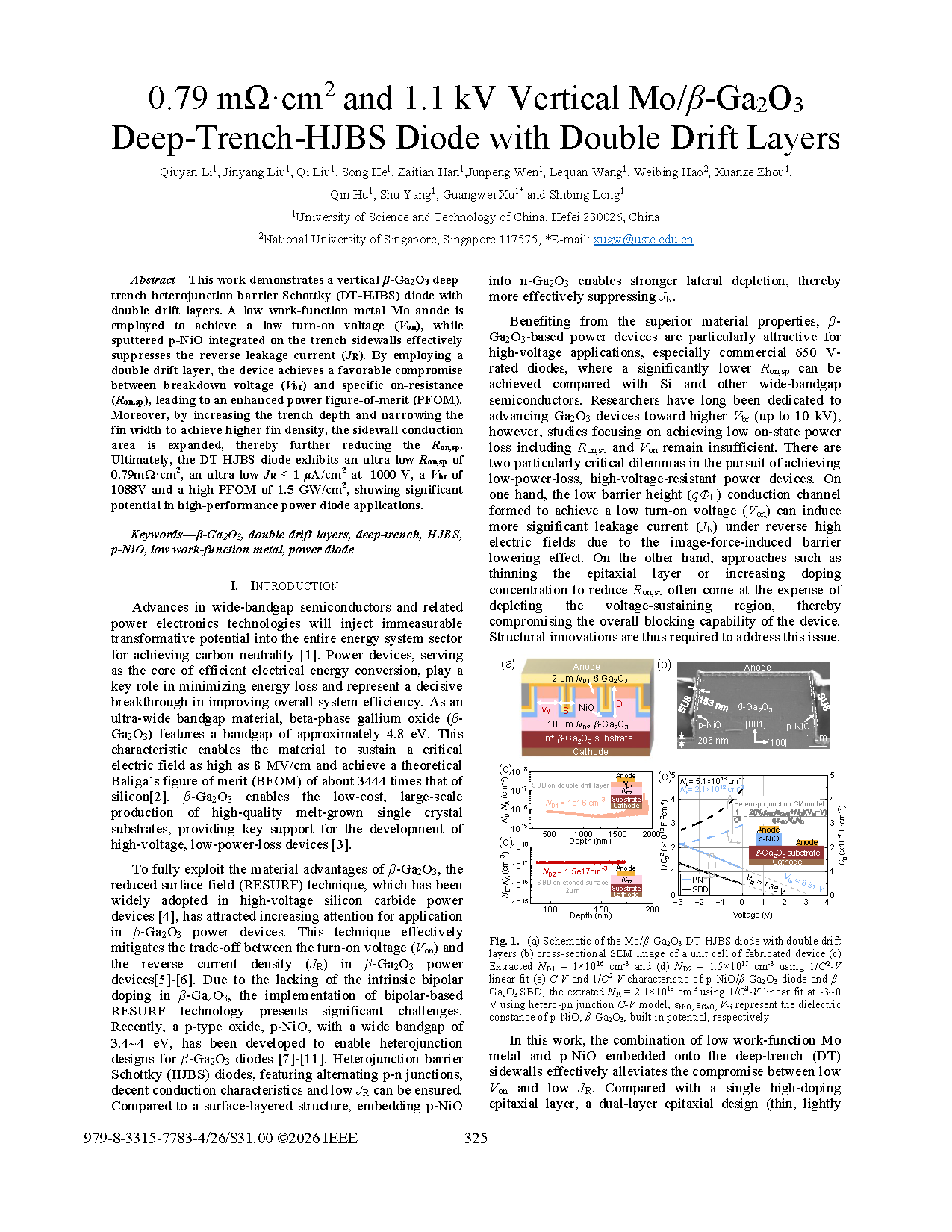
Fig. 1. (a) Schematic of the Mo/β-Ga₂O₃ DT-HJBS diode with double drift layers (b) cross-sectional SEM image of a unit cell of fabricated device.(c) Extracted ND1 = 1×10¹⁶ cm⁻³ and (d) ND2 = 1.5×10¹⁷ cm⁻³ using 1/C²-V linear fit (e) C-Vand 1/C²-V characteristic of p-NiO/β-Ga₂O₃ diode and β-Ga₂O₃ SBD, the extrated NA=2.1×10¹⁵ cm⁻³ using 1/C-V linear fit at -3~0 V using hetero-pn junction C-V model, εNKO, εGO, Vbi represent the dielectric constance of p-NiO, β-Ga₂O₃, built-in potential, respectively.
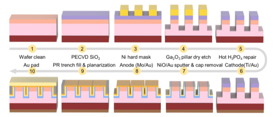
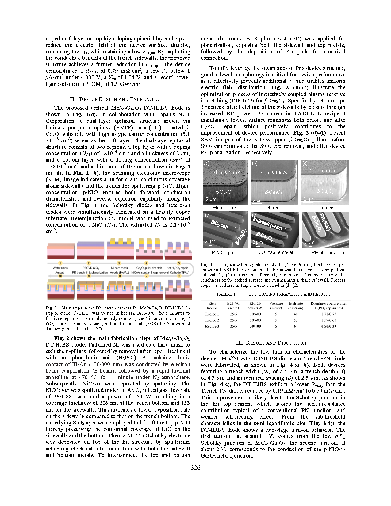
Fig. 2. Main steps in the fabrication process for Mo/β-Ga₂O₃ DT-HJBS.
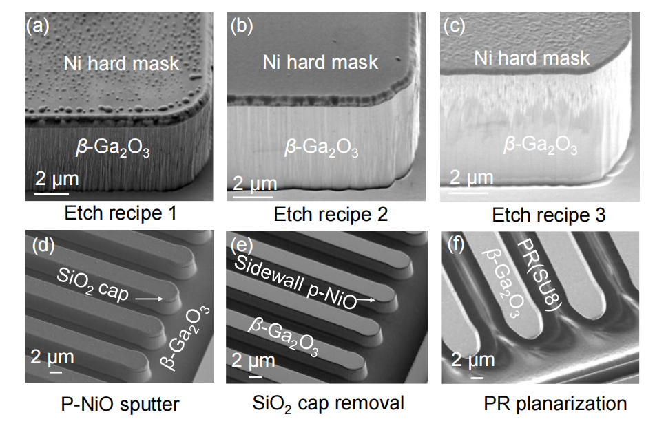
Fig. 3. (a)-(c) show the dry etch results for β-Ga₂O₃ using the three recipes shown in TABLE I. By reducing the RF power, the chemical etching of the sidewall by plasma can be effectively minimized, thereby reducing the roughness of the etched surface and maintaining a sharp sidewall. Process steps 7-9 outlined in Fig. 2 are illustrated in (d)-(f).
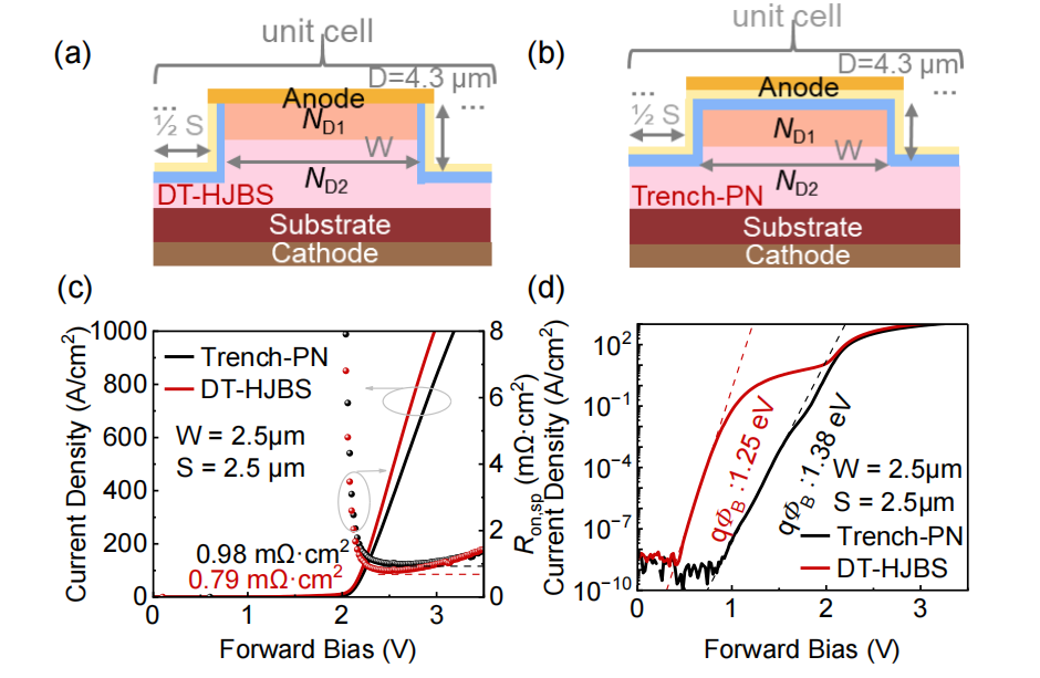
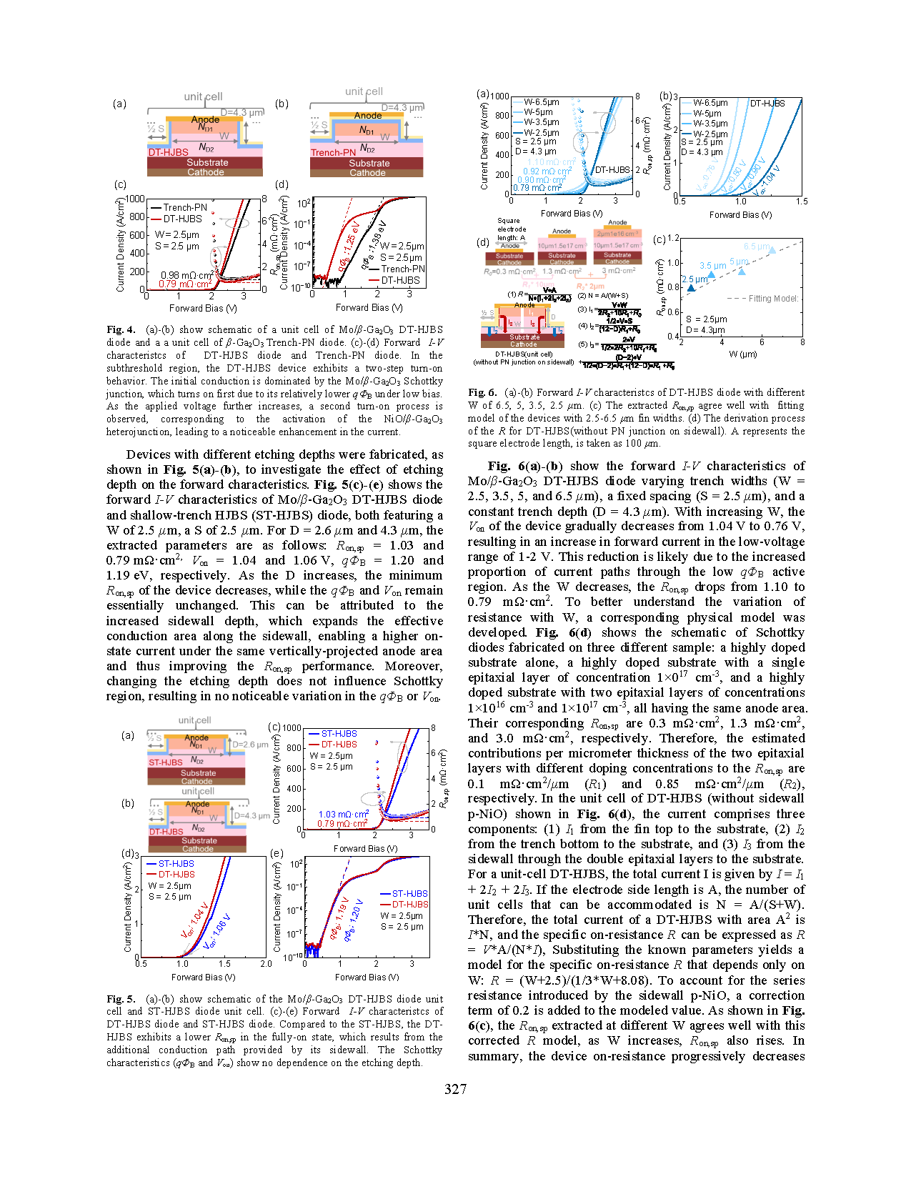
Fig. 4. (a)-(b) show schematic of a unit cell of Mo/β-Ga₂O₃ DT-HJBS diode and a unit cell of β-Ga₂O₃ Trench-PN diode. (c)-(d) Forward I-V characteristcs of DT-HJBS diode and Trench-PN diode. In the subthreshold region, the DT-HJBS device exhibits a two-step turn-on behavior. The initial conduction is dominated by the Mo/β-Ga₂O₃ Schottky junction, which turns on first due to its relatively lower qΦB under low bias. As the applied voltage further increases, a second turn-on process is observed, corresponding to the activation of the NiO/β-Ga₂O₃ heterojunction, leading to a noticeable enhancement in the current.
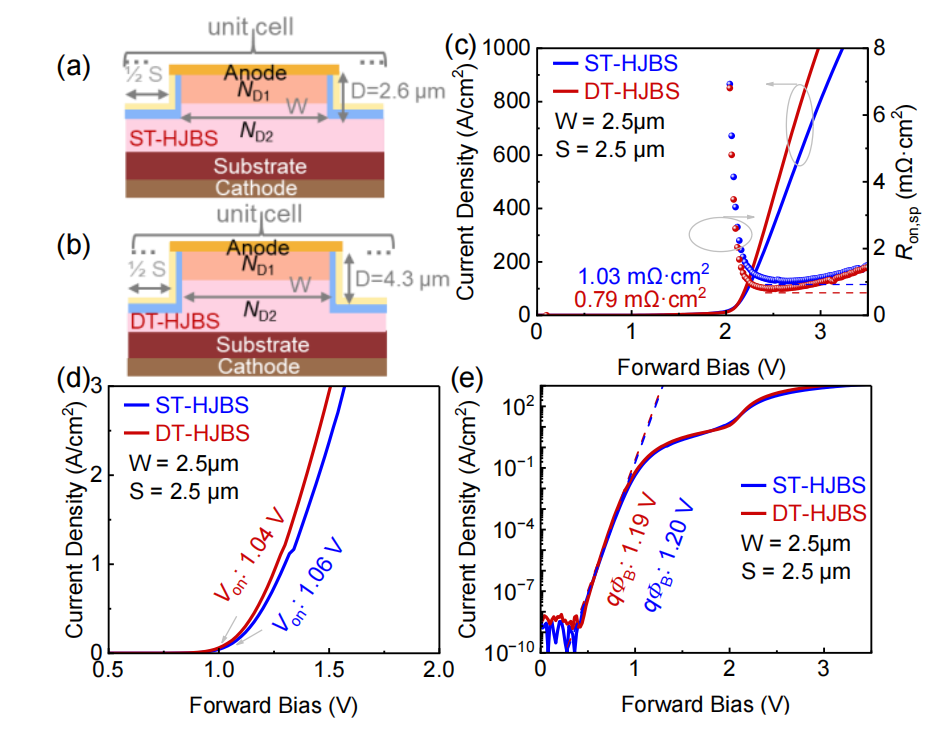
Fig. 5. (a)-(b) show schematic of the Mo/β-Ga₂O₃ DT-HJBS diode unit cell and ST-HJBS diode unit cell. (c)-(e) Forward I-V characteristcs of DT-HJBS diode and ST-HJBS diode. Compared to the ST-HJBS, the DT-HJBS exhibits a lower Ron,sp in the fully-on state, which results from the additional conduction path provided by its sidewall. The Schottky characteristics (qΦB and Von) show no dependence on the etching depth.
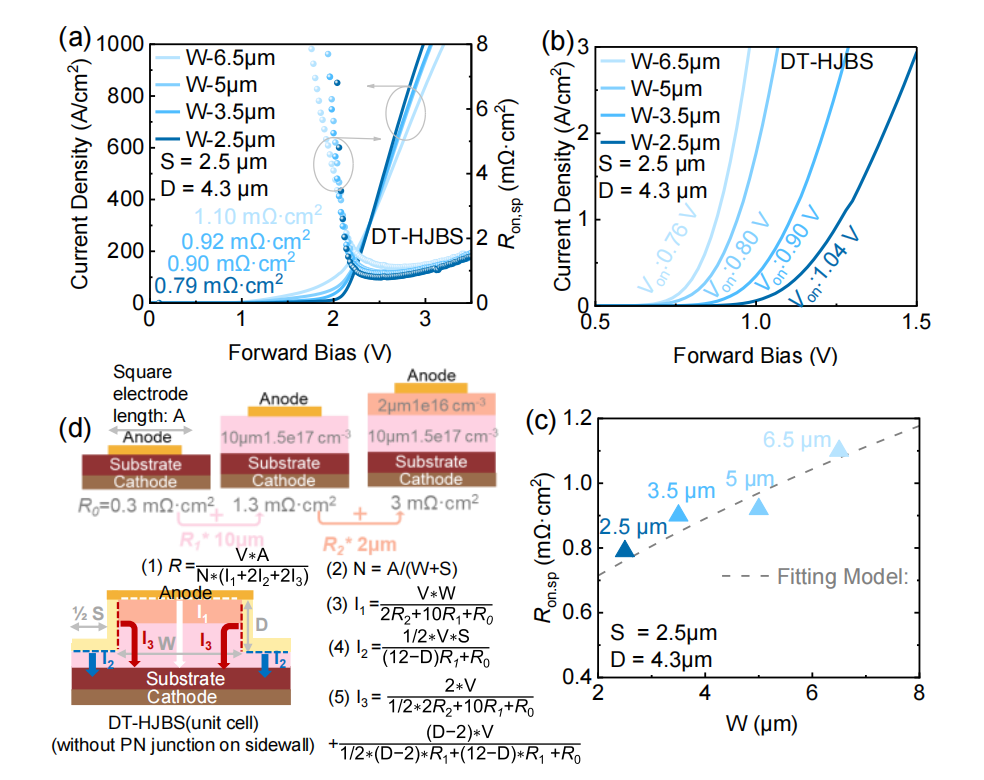
Fig. 6. (a)-(b) Forward I-V characteristcs of DT-HJBS diode with different W of 6.5, 5, 3.5, 2.5 μm. (c) The extracted Ron,sp agree well with fitting model of the devices with 2.5-6.5 μm fin widths. (d) The derivation process of the R for DT-HJBS (without PN junction on sidewall). A represents the square electrode length, is taken as 100 μm.
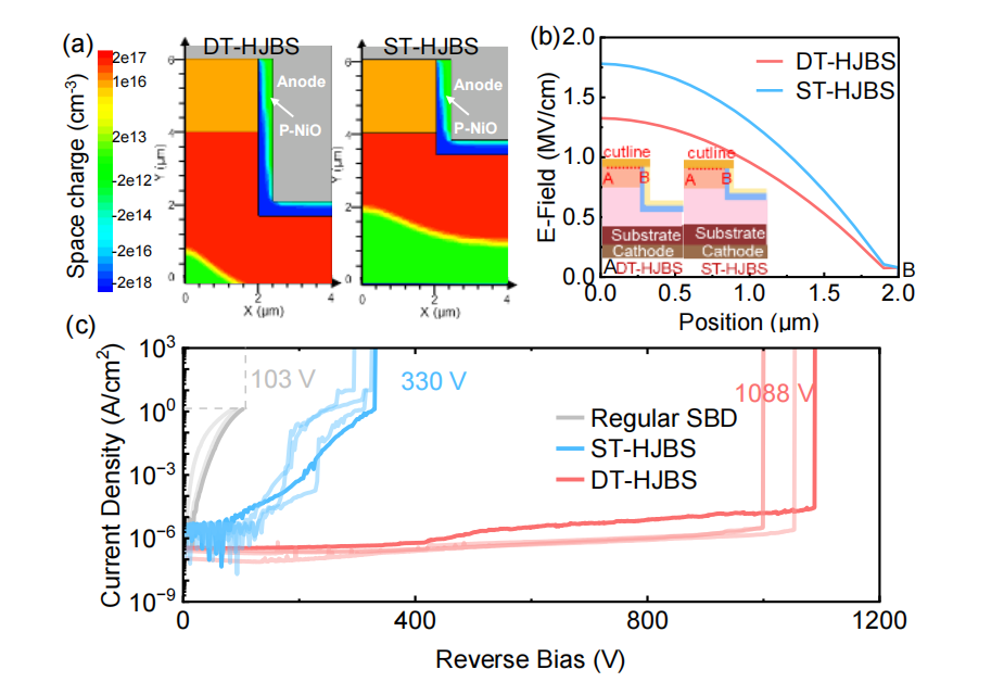
Fig. 7. (a) Simulated space charge of distribution of DT-HJBS, ST-HJBS devices under -1000 V. The electrical field extracted along the top horizontal cutline (A-B) for the DT-HJBS and ST-HJBS at -1000 V, inset shows the cutline of devices. Reverse I-V characteristics comparison among Regular SBD, ST-HJBS, DT-HJBS devices.
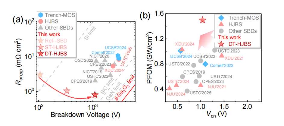
Fig. 8. Benchmark plot of (a) Ron,sp vs. Vbr and (b) PFOM vs. Von for the state-of-the-art vertical β-Ga₂O₃ diodes.
DOI:
10.1109/ISPSD64561.2026.11553594
Instruction
Official Account

Cooperation
Top
