


Researchers from Slovak Academy of Sciences, Czech Academy of Sciences, University of Bristol, HUN-REN Centre for Energy Research have published a dissertation titled "Heterogeneous integration of β-Ga₂O₃ and polycrystalline diamond via SiC and SiO₂ interlayers with optimized adhesion and thermal boundary resistance for power-electronic applications" in Carbon.
Background
Monoclinic β-Ga₂O₃ is a promising candidate for high-power electronics, yet its intrinsic low thermal conductivity causes severe junction overheating under high current, resulting in thermal stress-induced cracks and premature device failure. Polycrystalline diamond with ultrahigh thermal conductivity is an ideal heat sink material, while direct diamond growth on β-Ga₂O₃ brings fatal issues including large lattice/thermal expansion mismatch and plasma-induced Ga₂O₃ degradation. Previous reports only adopt either SiO₂ or Si single interlayer without systematic trade-off analysis on adhesion and thermal boundary resistance. Three mainstream diamond seeding methods (nanodiamond, ultrasonic, polymer-assisted) have not been quantitatively compared on interface microstructure and heat dissipation performance. No standardized two-step diamond growth route balancing strong bonding and low TBR is reported for industrial linear antenna microwave CVD, forming a critical research gap in thermal management of Ga₂O₃ power devices.
Abstract
Efficient thermal management is critical for reliable ultrawide-bandgap β-Ga₂O₃ devices, as their intrinsically low thermal conductivity limits high-power operation. Integration with diamond, a material with exceptional thermal conductivity, provides a promising pathway for heat dissipation; however, achieving high-quality β-Ga₂O₃/diamond interfaces remains challenging due to thermal expansion and lattice mismatches, as well as β-Ga₂O₃ degradation during harsh-environment and high-temperature diamond growth. In this work, we investigate β-Ga₂O₃/diamond heterostructures consisting of epitaxial β-Ga₂O₃ films on c-plane sapphire, nanocrystalline diamond layers deposited by chemical vapor deposition, and intermediate SiO₂ or SiC layers. Three diamond seeding approaches (nanodiamond, ultrasonic, and polymer-assisted) were evaluated to determine their impact on diamond quality, thermal boundary resistance (TBR), and mechanical adhesion. The structures were comprehensively characterized using X-ray diffraction, electron microscopy, scratch adhesion testing, and time-domain thermoreflectance measurements. Our results demonstrate that both the interlayer material and the seeding technique strongly influence interface quality, mechanical stability, and thermal transport. SiO₂-based structures exhibited the lowest effective TBR (~47 m² K/GW), while SiC interlayers provided superior mechanical adhesion. The overall thermal resistance was found to be primarily governed by the buried interlayer and its associated interfaces. Based on these findings, we propose an optimized two-step β-Ga₂O₃/diamond integration approach, employing a thin protective nanocrystalline diamond layer followed by highly-thermally-conductive diamond overgrowth. When maintained at thicknesses of 20 – 50 nm, the initial nanocrystalline diamond layer contributes only ~3 – 9 m² K/GW to the total thermal resistance. This approach establishes an optimized interface-forming technological platform for future β-Ga₂O₃-based power device applications.
Highlights
Systematically compare SiO₂and SiC interlayers for β-Ga₂O₃/diamond integration, quantitatively reveal trade-off between thermal boundary resistance and mechanical adhesion.
Evaluate three industrial diamond seeding techniques (NDS/US/PAS) on diamond crystallinity, interface voids and cross-plane thermal transport performance.
Confirm SiO₂interlayer with ultrasonic seeding achieves minimum TBR of 47 m² K/GW; SiC interlayer delivers 2x higher critical scratch load for robust packaging.
Propose scalable two-step diamond heteroepitaxy process with 20–50 nm protective nanodiamond buffer to avoid Ga₂O₃ plasma damage.
Conclusion
In this work, we demonstrated heterogeneous integration of the LI-MOCVD-grown heteroepitaxial (201) β-Ga₂O₃ with linear-antenna microwave CVD-grown polycrystalline diamond using thin SiO₂ and SiC interlayers and three nanodiamond seeding techniques (NDS, US, and PAS). We comprehensively analyzed the critical β-Ga₂O₃/interlayer/diamond interfaces and identified the primary factors controlling heterostructure performance.
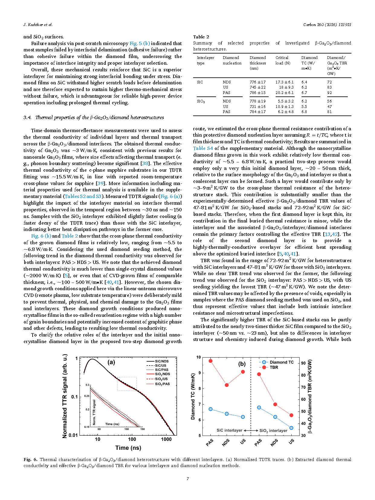
The interlayer material and seeding method jointly control the tradeoff between thermal and mechanical performance. SiC interlayer provided enhanced adhesion (critical loads ~17–20 N) compared to SiO₂ interlayer (~6–11 N), whereas SiO₂ interlayer yielded lower β-Ga₂O₃/diamond TBR (47–81 m² K/GW vs. 72–92 m² K/GW for SiC). For SiO₂, the US seeding route produced the lowest TBR (47 m² K/GW) and minimal void formation, indicating the most favorable interface quality. The diamond films grown under the selected mild linear-antenna microwave CVD conditions exhibited relatively low thermal conductivity (~7 W/m⋅K), reflecting their nanocrystalline character. However, these growth conditions effectively protected the β-Ga₂O₃ and the interlayers during diamond growth, while achieving competitive TBR and good mechanical stability.
Based on these findings, we propose a clearly defined two-step diamond growth approach for future β-Ga₂O₃/diamond device structures. In the first step, a thin (20 – 50 nm) continuous nanocrystalline diamond layer is grown under mild low-temperature linear-antenna microwave CVD conditions to protect the β-Ga₂O₃/interlayer stack, form an adherent buried interface, and to provide nucleation sites for high-quality diamond overgrowth. In the second step, conventional high-temperature microwave-plasma CVD is used to deposit a thicker, highly-thermally-conductive microcrystalline diamond overlayer for efficient heat spreading. The present work addresses and optimizes the first, interface-forming step. The thin (20 – 50 nm) initial nanocrystalline diamond layer adds only ~3 – 9 m² K/GW to the thermal resistance of the heterostructure, confirming that the interlayer and associated buried interfaces dominate the effective TBR. The presented structures are considered optimized high-quality interface-forming platforms that provide a practical pathway for future β-Ga₂O₃/diamond integration using scalable and industry-compatible processes.
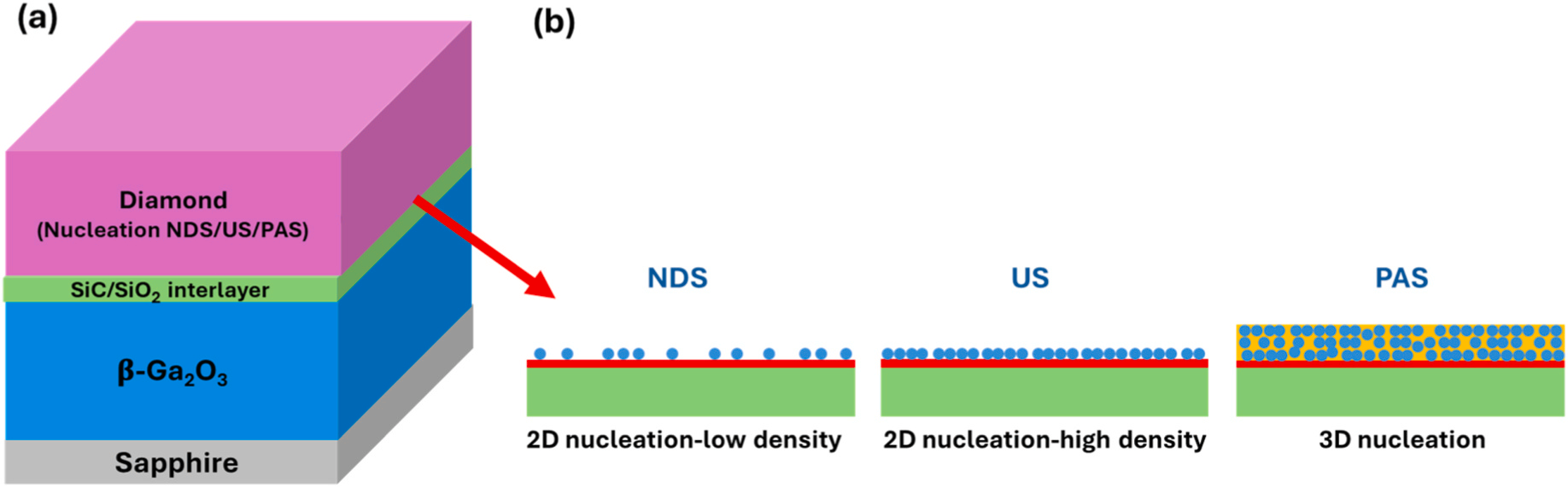
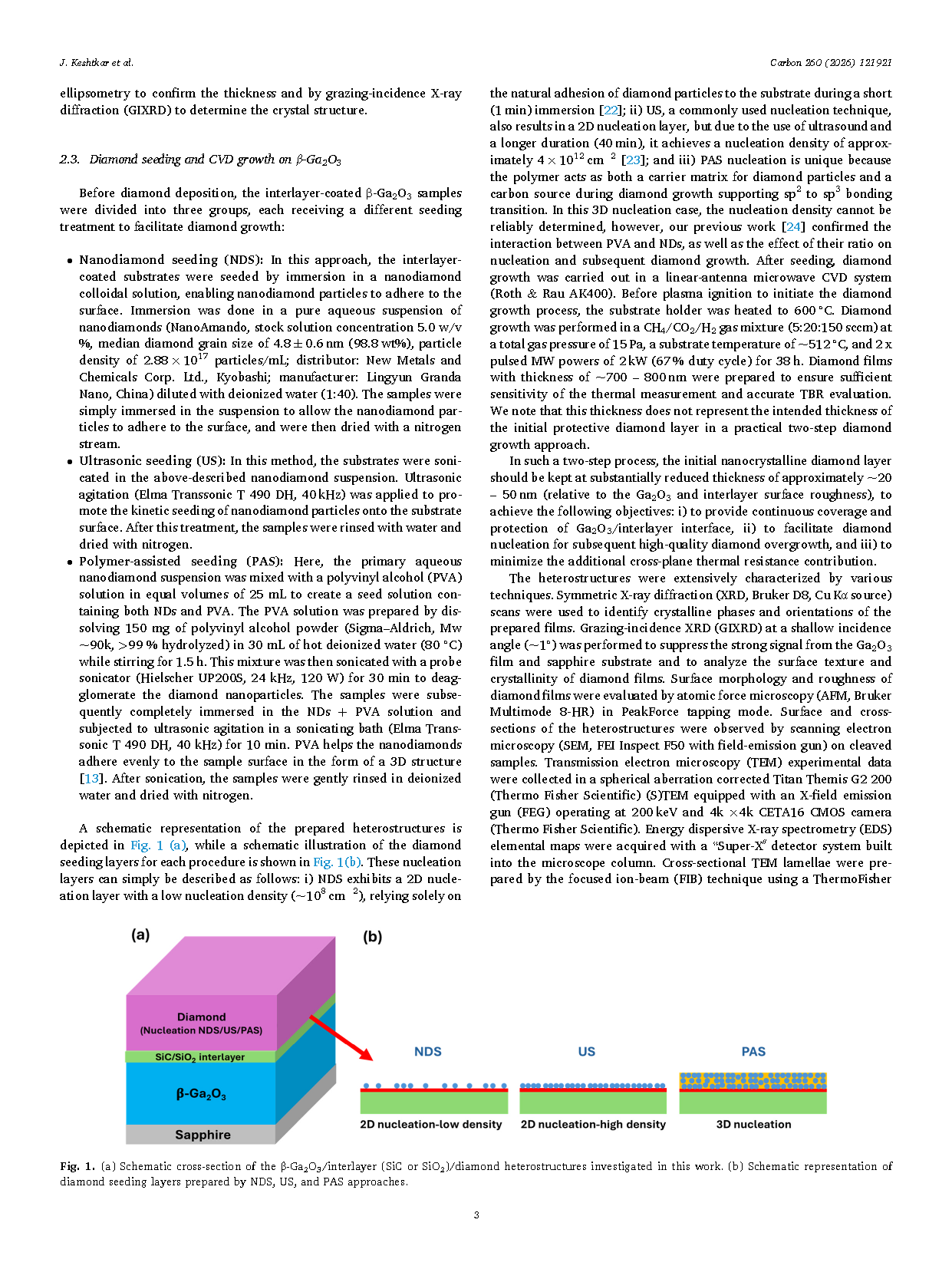
Fig. 1. (a) Schematic cross-section of the β-Ga₂O₃/interlayer (SiC or SiO₂)/diamond heterostructures investigated in this work. (b) Schematic representation of diamond seeding layers prepared by NDS, US, and PAS approaches.
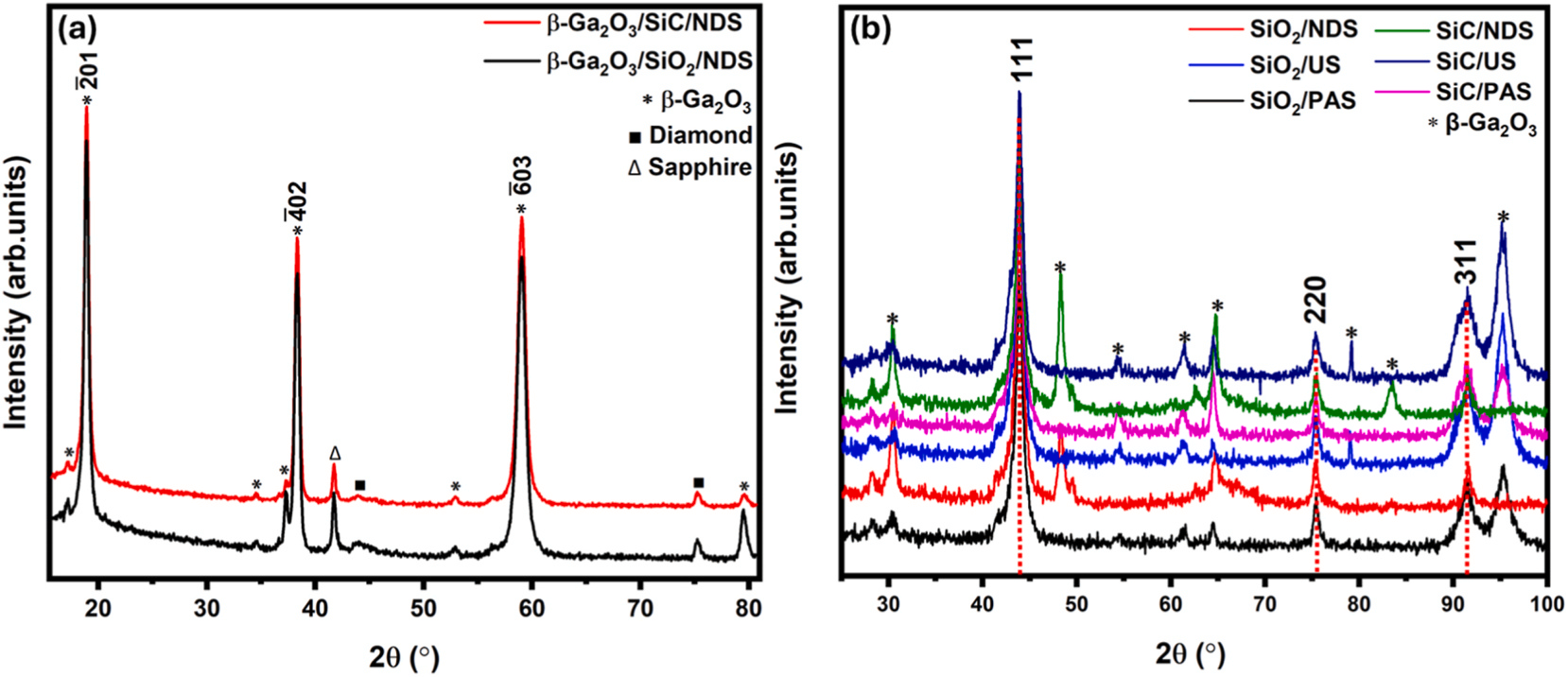
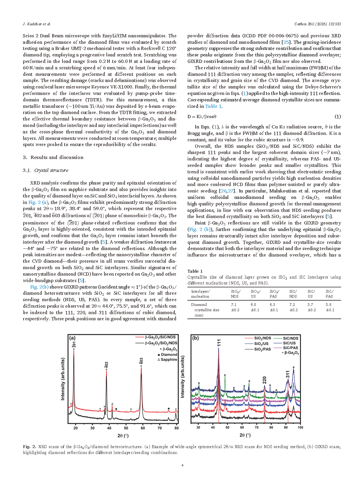
Fig. 2. (a) Example of wide-angle symmetrical 2θ/ω XRD scans for NDS seeding method, (b) GIXRD scans, highlighting diamond reflections for different interlayer/seeding combinations.
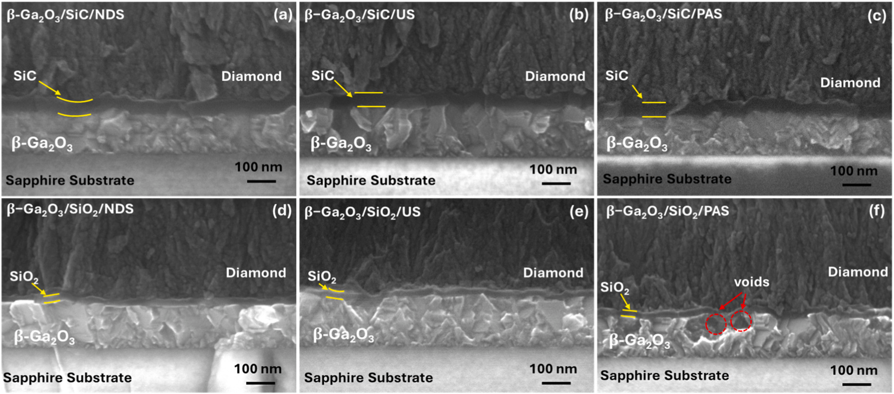
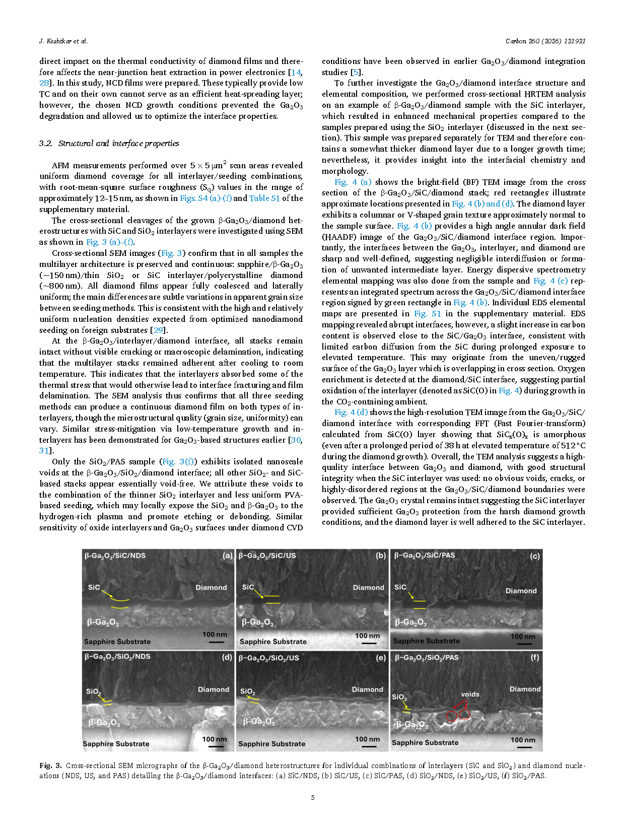
Fig. 3. Cross-sectional SEM micrographs of the β-Ga₂O₃/diamond heterostructures for individual combinations of interlayers (SiC and SiO₂) and diamond nucleations (NDS, US, PAS) detailing the β-Ga₂O₃/diamond interfaces: (a) SiC/NDS, (b) SiC/US, (c) SiC/PAS, (d) SiO₂/NDS, (e) SiO₂/US, (f) SiO₂/PAS.
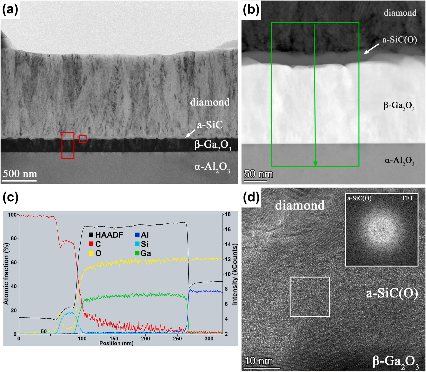
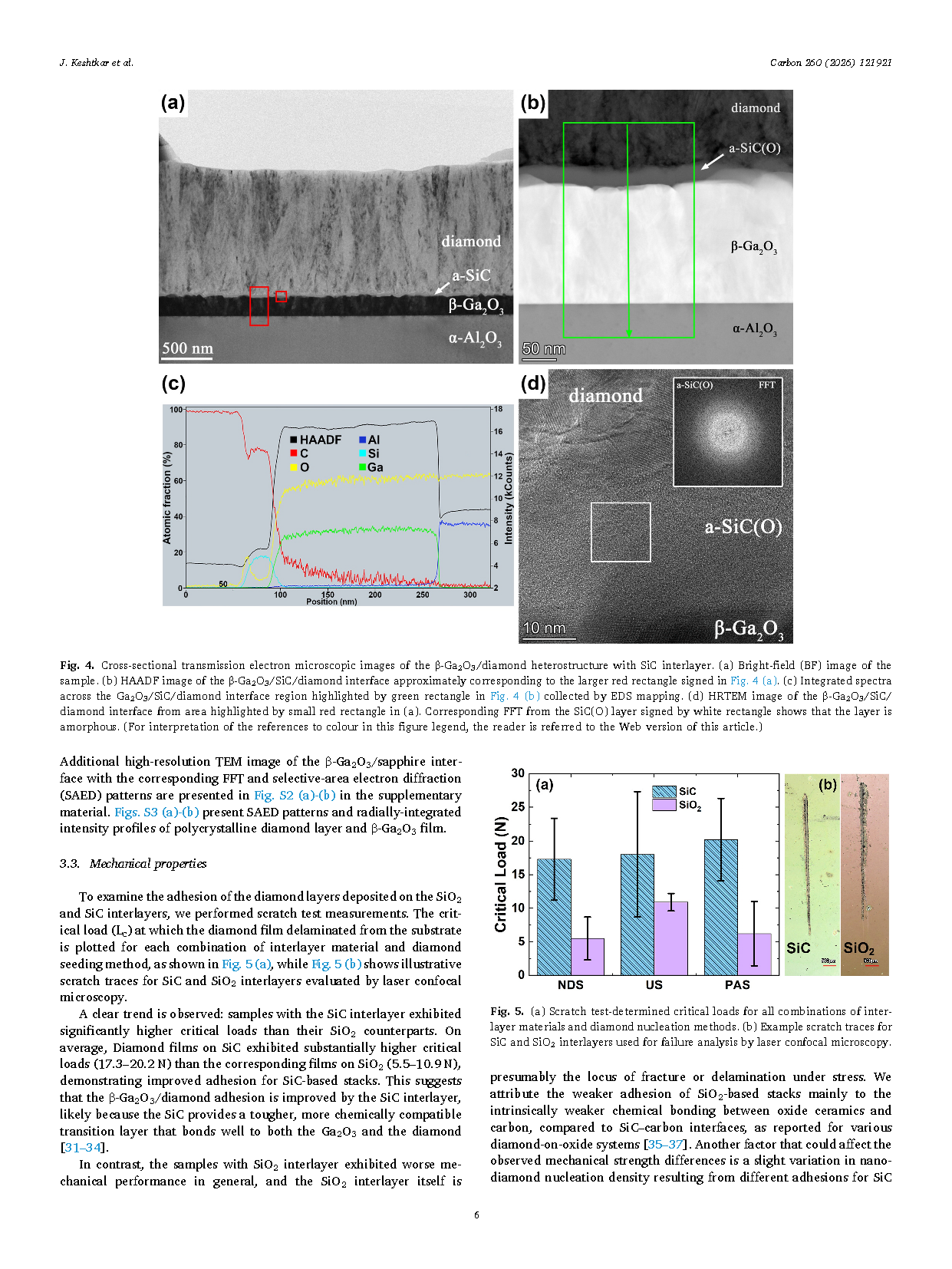
Fig. 4. Cross-sectional transmission electron microscopic images of the β-Ga₂O₃/diamond heterostructure with SiC interlayer. (a) Bright-field (BF) image of the sample. (b) HAADF image of the β-Ga₂O₃/SiC/diamond interface approximately corresponding to the larger red rectangle signed in Fig. 4 (a). (c) Integrated spectra across the Ga₂O₃/SiC/diamond interface region highlighted by green rectangle in Fig. 4 (b) collected by EDS mapping. (d) HRTEM image of the β-Ga₂O₃/SiC/diamond interface from area highlighted by small red rectangle in (a). Corresponding FFT from the SiC (O) layer signed by white rectangle shows that the layer is amorphous. (For interpretation of the references to colour in this figure legend, the reader is referred to the Web version of this article.)
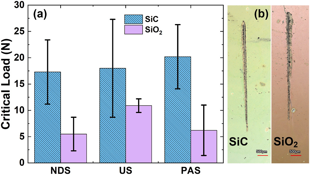
Fig. 5. (a) Scratch test-determined critical loads for all combinations of interlayer materials and diamond nucleation methods. (b) Example scratch traces for SiC and SiO₂ interlayers used for failure analysis by laser confocal microscopy.
DOI:
doi.org/10.1016/j.carbon.2026.121921
Instruction
Official Account

Cooperation
Top
