


Introduction:
In the previous issue, we started with the fundamental concepts of epitaxy and introduced the critical role of β-Ga₂O₃ epitaxial layers in regulating drift layer thickness, carrier concentration, and electric field distribution within devices. As the link between single-crystal substrates and power devices, epitaxial technology serves as a key bridge for translating the intrinsic advantages of β-Ga₂O₃ materials into device-level performance.
However, achieving a high-quality thin film in the laboratory is only the first step. There remains a significant gap between laboratory-scale epitaxial growth and the stable manufacturing of large-area, low-defect, and uniformly doped epitaxial wafers suitable for device fabrication. Especially for high-voltage power devices, epitaxial processes must not only ensure excellent crystal quality, but also simultaneously meet multiple requirements, including thick film growth, low carrier concentration, high in-wafer uniformity, excellent surface smoothness, and high production efficiency.
Among the various β-Ga₂O₃ epitaxial technologies, halide vapor phase epitaxy (HVPE) and metal-organic chemical vapor deposition (MOCVD) are widely regarded as two of the most promising routes for industrialization. HVPE features a high growth rate, making it well suited for fabricating the thick drift layers required in high-voltage vertical power devices. In contrast, MOCVD offers superior capabilities in doping, composition, and interface control, making it suitable for constructing precisely engineered functional layers in advanced devices. These two technologies represent different directions in epitaxial manufacturing: “high-efficiency thick-layer growth” and “precise material engineering.”
In this issue, we will further focus on the industrialization progress of β-Ga₂O₃ homoepitaxy, reviewing the latest developments of HVPE and MOCVD in areas including growth rate, substrate orientation, impurity and defect control, doping regulation, and device-level validation.
Epitaxial Industrialization:
Technological Breakthroughs and Practical Challenges of HVPE and MOCVD
Industrial Requirements for Homoepitaxy
For power devices, the epitaxial layer serves as the core region responsible for voltage blocking, current transport, and electric field regulation. Especially in vertical power devices, the thickness and carrier concentration of the lightly doped drift layer directly determine the device’s voltage withstand capability and on-resistance.
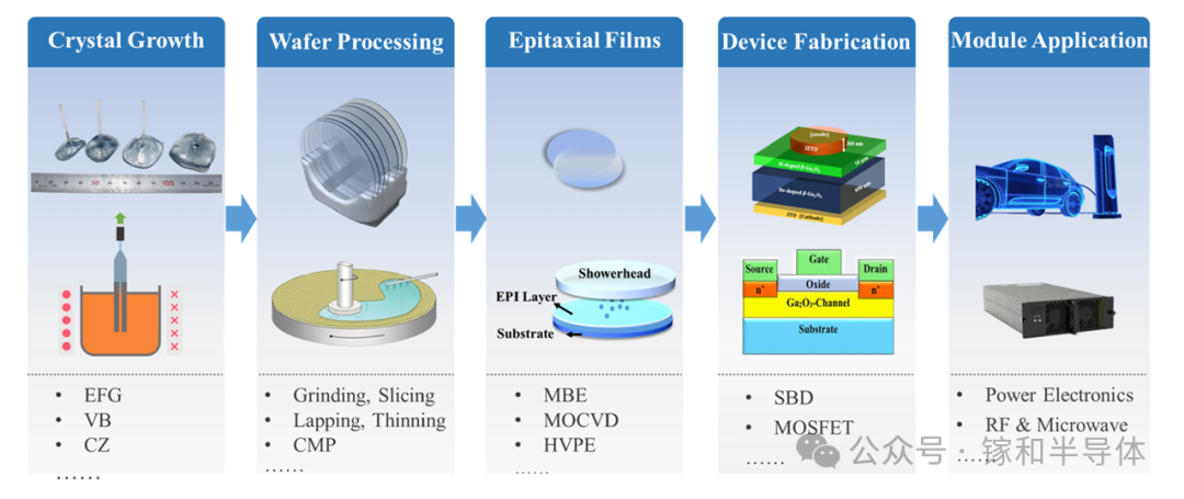
Figure 1. Manufacturing process flow of gallium oxide-based materials and devices [1]
Laboratory research typically focuses on parameters such as the growth rate, surface roughness, and X-ray diffraction full width at half maximum (FWHM) of individual samples. However, industrial-scale production requires addressing a broader range of challenges: Can the epitaxial layer maintain uniform thickness and doping concentration across large-area wafers? Can defect density be consistently controlled? Can the process achieve batch-to-batch reproducibility? Can the growth efficiency justify the costs of equipment, precursors, and post-processing? And can the epitaxial wafers be directly integrated into device fabrication processes?
The competition in β-Ga₂O₃ epitaxy is gradually shifting from breakthroughs in individual performance metrics toward a comprehensive balance among growth rate, material quality, process stability, and manufacturing cost.
Currently, HVPE and MOCVD are advancing industrialization along two distinct pathways: HVPE focuses on efficiently producing thick drift layers required for high-voltage vertical devices, while MOCVD emphasizes achieving device-grade functional structures through precise control of precursor flow, doping, and interface engineering.
HVPE: High-Speed Thick-Film Growth
High Growth Rate
The Core Advantage of HVPE
HVPE typically uses gallium halides such as GaCl as gaseous gallium sources, which react with O₂ on high-temperature substrates to form β-Ga₂O₃. Compared with metal-organic precursors, halide-based precursors feature a relatively direct reaction pathway, lower material costs, and higher mass transport efficiency, making HVPE particularly suitable for the growth of epitaxial layers with thicknesses of tens of micrometers.
For vertical power devices rated at kilovolt levels or above, the drift layer thickness often needs to reach 10 μm or more. If the growth rate is too low, both the epitaxy time per wafer and equipment utilization costs increase rapidly. Therefore, HVPE has an inherent advantage in thick-film fabrication, with typical growth rates reaching 5–10 μm/h, and optimized processes achieving growth rates of several tens of micrometers per hour [2–4].
However, industrialization does not simply mean pursuing the highest possible growth rate. In conventional GaCl–O₂ systems, increasing precursor partial pressure can enhance the growth rate, but it may also increase the risk of gas-phase parasitic reactions, leading to the formation of polycrystalline β-Ga₂O₃ particles. Once these particles deposit onto the epitaxial surface, they may trigger abnormal growth and locally degrade surface morphology [3,5].
Meanwhile, large-scale epitaxial production still requires further solutions for maintaining within-wafer uniformity in film thickness, carrier concentration, and surface morphology, which remain critical challenges for HVPE industrialization.
Substrate Orientation
Impacting Growth Efficiency and Defect Evolution
β-Ga₂O₃ exhibits pronounced crystal anisotropy. The atomic arrangement, surface energy, adsorption behavior, and step-flow kinetics vary significantly among different crystal planes. As a result, substrate orientation directly influences the growth rate, surface morphology, and defect evolution of epitaxial layers.
Currently, the (001)-oriented substrate has a relatively mature foundation in large-area substrate supply and represents an important direction for β-Ga₂O₃ HVPE industrialization. However, epitaxial growth on this orientation is prone to forming stripe-like grooves extending along the [010] direction [6]. In addition, some defects are associated with the propagation of substrate dislocations, meaning that further improvements are still required in surface morphology and device yield.
Meanwhile, epitaxial growth on other substrate orientations, including (-201), (100), and (011) planes, has also achieved continuous progress, providing additional pathways for optimizing β-Ga₂O₃ epitaxial quality and device performance.
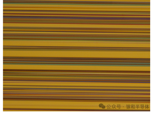
Figure 2. NDIC microscopy image of an 8 μm-thick HVPE homoepitaxial layer grown on a (001)-oriented β-Ga₂O₃ substrate [6]
According to reports, when (011)-oriented β-Ga₂O₃ was grown by HCl-based HVPE, the growth rate reached approximately 14 μm/h, which is about 60% of the growth rate achieved on (001)-oriented substrates under the same system. Meanwhile, compared with earlier Cl₂-based processes, the HCl-based approach improved the growth rate by approximately 5–7 times and significantly reduced the formation of surface polycrystalline particles [3].
The exploration of different substrate orientations is not solely aimed at achieving higher growth rates. More importantly, it seeks to establish the optimal relationship among crystal orientation, defect propagation behavior, and device structures, providing a pathway toward high-quality and scalable β-Ga₂O₃ epitaxial manufacturing.
Growth Condit
Balancing Growth Rate, Morphology, and Crystal
During HVPE epitaxial growth, parameters including growth temperature cdeposi.
Growth t determines the fundathree-dim. In contrast, excessivelysubstrate surface decomposition, interface instability, and increased defect formation. Therefore, temperature optimization requires a careful balance among gas-phase reaction efficiency, surface diffusion, and high-temperature desorption processes.
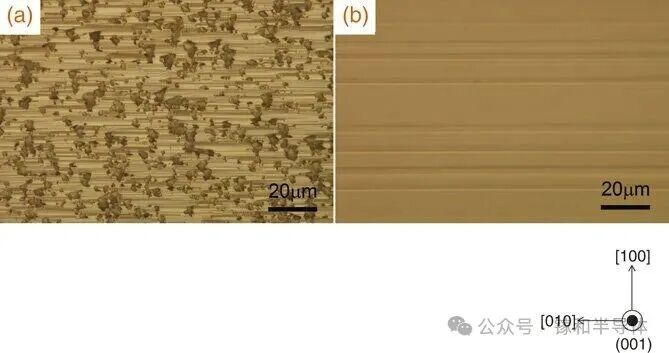
Figure 3. NDIC surface morphologies of (001)-oriented β-Ga₂O₃ HVPE homoepitaxial layers grown at different temperatures (left: 800 °C; right: 1000 °C) [7]
The VI/III ratio and precursor supply jointly determine the reaction driving force, local supersaturation, and mass transport processes in the GaCl–O₂ system [8,9]. Insufficient oxygen supply may prevent complete oxidation of the gallium precursor, resulting in an oxygen-deficient growth environment and increasing the risk of non-stoichiometric defects and related defect formation. Increasing the O₂/GaCl ratio helps maintain sufficient oxidation conditions; however, an excessively high oxidant partial pressure, especially under conditions of high GaCl partial pressure, elevated reaction pressure, or prolonged gas residence time, may enhance gas-phase precursor reactions, thereby affecting the effective transport and utilization efficiency of gallium species toward the substrate.
On the other hand, increasing the GaCl partial pressure within an appropriate range can enhance the growth rate. However, excessive reactant concentration may promote the formation of gas-phase particles and their transport toward the growth surface, leading to surface defects and morphological degradation. Therefore, the VI/III ratio is not simply a parameter where “higher is better”; its optimal range must be carefully coordinated with growth temperature, pressure, precursor partial pressures, total flow rate, and reactor design.
Reaction pressure further regulates precursor residence time, mass transport efficiency, and surface growth modes. According to reported studies, during (001)-oriented β-Ga₂O₃ homoepitaxial growth, reducing the pressure from 6.06 × 10⁴ Pa to 1.01 × 10⁴ Pa decreased the growth rate from 10.1 μm/h to 2.1 μm/h. The authors attributed this reduction to the decreased partial pressures of source gases such as GaCl and O₂ under lower pressure conditions, which reduced the effective reactant flux participating in surface reactions per unit time, thereby lowering the epitaxial growth rate.
However, moderately reducing the pressure can also suppress gas-phase parasitic reactions and particle formation, improving precursor transport toward the substrate surface. This promotes a transition in growth mode from three-dimensional island growth to two-dimensional step-flow growth, resulting in more continuous and refined surface striations. Under a pressure of 2.02 × 10⁴ Pa, the epitaxial layer achieved an X-ray diffraction rocking curve full width at half maximum (FWHM) of 30.2″, approaching that of the substrate (28.9″).
Therefore, although lowering pressure may sacrifice part of the growth rate due to reduced precursor partial pressure, it can effectively suppress gas-phase pre-reactions and particle defects, while improving the surface morphology and crystalline quality of β-Ga₂O₃ epitaxial layers.
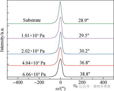
Figure 4. X-ray diffraction (XRD) rocking curves of the (001) planes of β-Ga₂O₃ substrates and epitaxial films grown under different pressures [10]
The gas flow field and reactor structure determine whether the optimized growth conditions can be uniformly achieved across large-area wafers. Even when the central region of a wafer maintains appropriate temperature, VI/III ratio, and pressure conditions, significant variations in boundary layer thickness, precursor concentration, or gas residence time across different regions of the wafer can still lead to non-uniformity in film thickness, surface morphology, and doping concentration.
Therefore, for industrial-scale β-Ga₂O₃ epitaxy, further optimization of the reactor design, including the distribution of temperature fields, concentration fields, and gas flow fields, is essential to minimize variations between the wafer center and edge, as well as improve batch-to-batch reproducibility.
Evolution from Cl₂-HVPE to HCl-HVPE and THVPE
Traditional Cl₂-HVPE typically utilizes the reaction between Cl₂ and liquid Ga to generate GaCl, which is then transported to the growth zone and reacts with O₂ to form β-Ga₂O₃ [3,7]. This approach features high reaction activity and relatively low material costs, making it suitable for rapid growth of thick epitaxial layers. However, under high precursor partial pressure conditions, GaCl and O₂ may undergo parasitic gas-phase reactions before reaching the substrate, generating polycrystalline Ga₂O₃ particles. Once deposited onto the epitaxial surface, these particles can interfere with normal single-crystal growth, resulting in polycrystalline particles, local protrusions, or abnormal growth regions, thereby degrading epitaxial crystal quality [3,11].
HCl-based HVPE generates GaCl through the reaction between HCl and metallic Ga, with H₂ produced as a by-product. In this system, additional HCl can be introduced into the growth zone to regulate the balance between growth and etching. By selectively etching parasitic Ga₂O₃ deposits, the process can reduce the formation of gas-phase particles and unwanted deposition. However, the HCl-based route remains a chlorine-containing chemical system accompanied by hydrogen-containing by-products. Issues including chlorine incorporation, Si contamination from quartz reactor components, corrosion resistance of equipment, and exhaust gas treatment still require careful control through optimization of growth temperature, gas flow, and reactor structure [3,12,13].
Another emerging route is trihalide vapor phase epitaxy (THVPE), which directly uses GaCl₃ as the gallium precursor. Unlike Cl₂- or HCl-based HVPE, THVPE does not rely on continuous in-reactor chlorination of metallic Ga. Instead, pre-generated GaCl₃ is directly delivered to the growth zone, simplifying the metal source reaction process and potentially reducing source-zone particle formation and precursor supply fluctuations. Previous studies have demonstrated that THVPE can achieve growth rates of several tens of micrometers per hour, highlighting its potential for the fabrication of thick drift layers required for high-voltage power devices [14].
Industrialization Challenges:
Impurities, Defects, and Post-Growth Processing
Typical background impurities in HVPE-grown β-Ga₂O₃ epitaxial layers include Cl, N, and Si. Among them, Cl mainly originates from halide-based precursors, N may be introduced from chamber background impurities and growth atmosphere, while Si is often released from quartz reactor components under high-temperature conditions.
Studies have shown that by increasing the O₂ partial pressure and the input VI/III ratio [10], the unintentional N impurity concentration in HVPE-grown β-Ga₂O₃ epitaxial layers can be reduced from approximately 8 × 10¹⁶ cm⁻³ to around 1 × 10¹⁶ cm⁻³. Defect spectroscopy and first-principles calculations have further demonstrated that N can substitute for O sites in β-Ga₂O₃ and form deep acceptor defects, with N occupying the O(III) site being a relatively stable configuration [15]. Therefore, increasing the oxygen chemical potential may suppress N incorporation by reducing the formation probability and incorporation tendency of N-related oxygen substitution defects.
For Si impurities, reactions between hydrogen-containing species and high-temperature quartz reactor walls may lead to Si release. This issue can be mitigated by reducing reactor wall temperature, minimizing quartz component exposure, or introducing protective liner structures.
In addition to impurity incorporation, HVPE epitaxy may suffer from defects including particle-induced defects, deep pits, line defects, dislocations, and localized polycrystalline regions. Although these defects may occupy only a small fraction of the wafer area, they can act as reverse leakage paths in devices, significantly reducing breakdown voltage and wafer yield.
Furthermore, HVPE-grown thick films typically exhibit relatively high surface roughness and often require chemical mechanical polishing (CMP) before entering device fabrication processes. While CMP can achieve a smoother surface, it may also introduce subsurface damage, abrasive residues, and within-wafer thickness variations. Therefore, for industrial-scale HVPE manufacturing, epitaxial growth and CMP should not be treated as independent processes, but rather optimized as an integrated and continuous fabrication workflow.
Device Validation Progress
Previous studies have demonstrated the potential of HVPE-grown β-Ga₂O₃ epitaxial layers for high-voltage power devices. Using an approximately 13 μm-thick HVPE-grown β-Ga₂O₃ drift layer, researchers fabricated p-NiOₓ/β-Ga₂O₃ heterojunction diodes with a breakdown voltage of 8.32 kV [16].
Further improvements were achieved by employing a thicker drift layer of approximately 17–18 μm with a net carrier concentration of around 8.8 × 10¹⁵ cm⁻³, combined with a double-layer SiNₓ/SiO₂ edge termination structure. The resulting devices with a diameter of 100 μm achieved a breakdown voltage of 13.5 kV, corresponding to an average critical electric field of approximately 7.4–9.4 MV/cm [17].
These results demonstrate that HVPE is capable of providing the thick, low-doped drift layers required for ten-kilovolt-class β-Ga₂O₃ power devices. However, device performance is determined not only by epitaxial layer thickness but also by the combined effects of carrier concentration and uniformity, defect and trap distribution, device area, and edge termination design.
As device dimensions increase, the probability of incorporating local defects and leakage pathways into the active region also rises, making it more challenging to maintain high breakdown voltage and wafer-level yield. Therefore, transitioning from small-area devices with record-breaking performance toward large-area, high-yield, and long-term reliable commercial products still requires further advances in wafer-scale epitaxial uniformity and defect control.
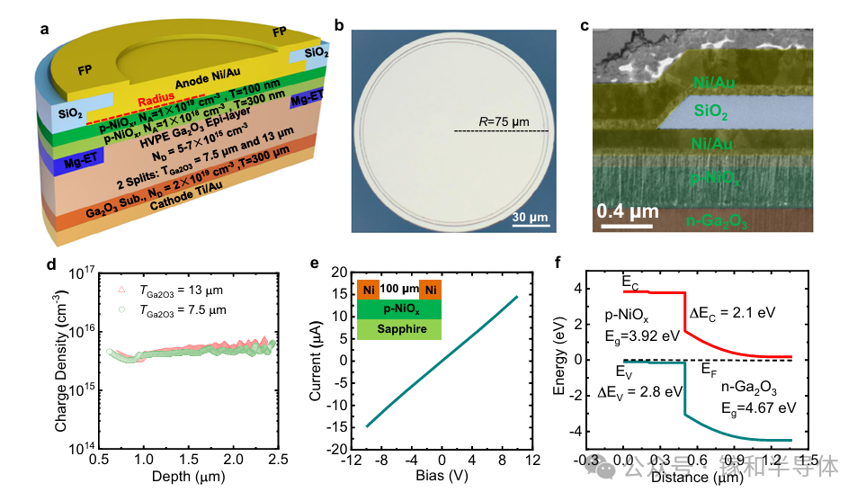
Figure 5. Device structures and performance of β-Ga₂O₃ devices based on HVPE epitaxial layers [16]
MOCVD: Precise Control
Precursor Selection
The commonly used gallium precursors for β-Ga₂O₃ MOCVD growth mainly include triethylgallium (TEGa) and trimethylgallium (TMGa).
TEGa was one of the earliest and most widely used precursors in β-Ga₂O₃ MOCVD research. Its process control is relatively mature, with typical growth rates of approximately 0.2–1.0 μm/h [18]. However, this growth rate is generally insufficient for high-efficiency thick-film fabrication.
In comparison, TMGa exhibits higher vapor pressure and greater potential for high-speed growth. By increasing TMGa supply and optimizing oxygen flow conditions, the MOCVD growth rate can reach 4–8 μm/h, with some studies approaching 10 μm/h [19,20], gradually narrowing the growth-rate gap between MOCVD and HVPE.
However, high-rate TMGa growth is often accompanied by an increased risk of carbon (C) impurity incorporation from methyl groups. When organic ligands and their decomposition products are not fully oxidized, carbon may remain in the epitaxial layer and affect carrier compensation and transport properties through different lattice sites or C–H complexes. Increasing the O₂ flow rate and O/Ga ratio can promote the oxidation of carbon-containing species and suppress C incorporation.
Studies have shown that increasing the O₂ flow rate to 2000 sccm reduced the carbon concentration in β-Ga₂O₃ epitaxial layers from approximately 10¹⁸ cm⁻³ to below 5 × 10¹⁶ cm⁻³. Under a growth rate of approximately 4.5 μm/h, the epitaxial layers achieved a room-temperature electron mobility of up to 190 cm²·V⁻¹·s⁻¹ [19].
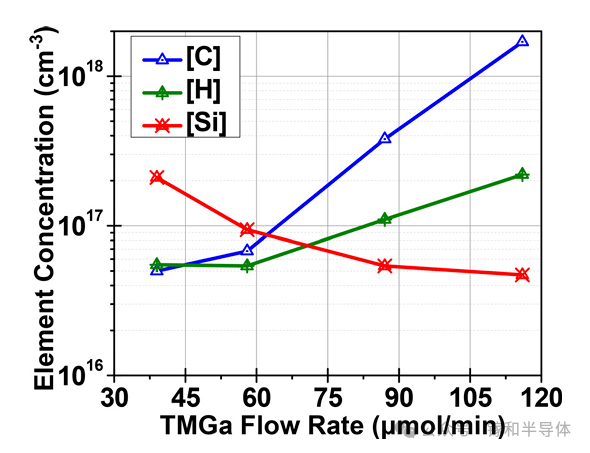
Figure 6. Relationship between C, H, and Si incorporation concentrations in β-Ga₂O₃ epitaxial layers and TMGa molar flow rate [20].
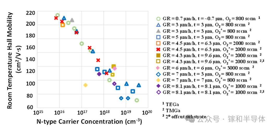
Figure 7. Relationship between room-temperature Hall mobility and electron concentration in (010)-oriented β-Ga₂O₃ epitaxial layers grown at high rates using TMGa [19].
Key Advantage: Precise Doping
ControlMOCVD enables dynamic control of dopant concentration and distribution within epitaxial layers through rapid and precise adjustment of gas flow rates.
Silicon (Si) is the most commonly used shallow donor dopant in β-Ga₂O₃. By adjusting the ratio between the silicon precursor and gallium precursor, the Si doping concentration and net carrier concentration can be controlled over a wide range, enabling the fabrication of drift layers, contact layers, and step-doped structures.
Studies have demonstrated that in multilayer calibration structures consisting of approximately 200–400 nm-thick sublayers, segmented adjustment of silicon precursor supply allows the Si concentration profile along the epitaxial growth direction to form well-defined plateau-like or step-like distributions [19].
This capability is highly important for device fabrication. For example, high-voltage power devices require lightly doped drift layers to sustain the electric field, while heavily doped contact layers are needed to reduce ohmic contact resistance. MOCVD can continuously grow different functional layers within a single epitaxial growth process, thereby reducing interface contamination and process transfer losses.
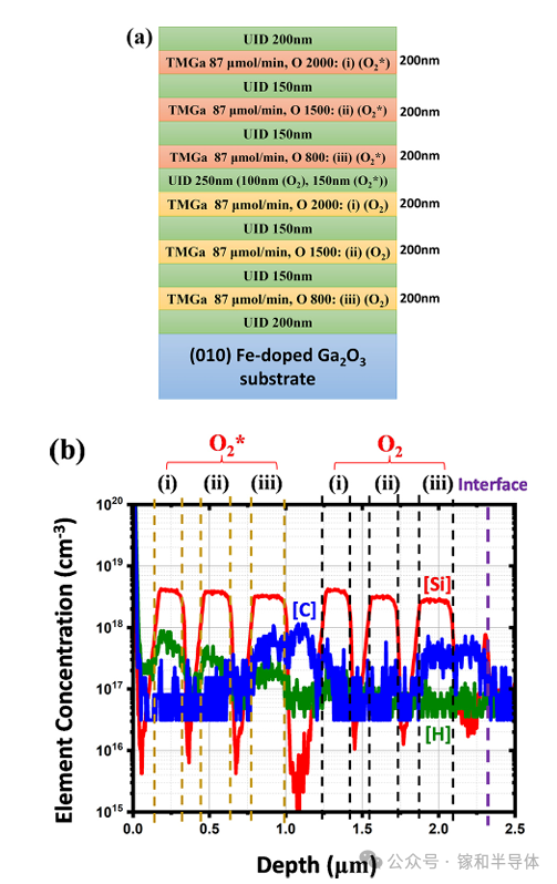
Figure 8. (a) Schematic structure of β-Ga₂O₃ multilayer SIMS samples consisting of alternating Si-doped layers and UID layers grown under different oxygen source flow conditions; (b) SIMS depth profiles of C, H, and Si concentrations in the samples [19].
Unintentional doping in MOCVD-grown β-Ga₂O₃ epitaxial layers is mainly associated with H, C, and Si impurities. Hydrogen (H) may act as a shallow donor contributing to electrical conduction, but it can also form complexes with carbon (C), leading to compensation effects. Interstitial H has been reported to exhibit shallow donor behavior, while the electrical role of C strongly depends on its lattice site occupation [21].
Further TMGa-MOCVD studies have shown that H–C-related complexes can passivate certain C-related compensation effects, rather than simply introducing additional compensation centers [22]. Therefore, the carrier concentration obtained from room-temperature Hall measurements only represents the net result of the combined effects of donors, acceptors, and trap states, and cannot be directly interpreted as a measure of material purity.
A comprehensive evaluation of background impurities and their electrical impacts requires combined analysis using techniques such as secondary ion mass spectrometry (SIMS), temperature-dependent Hall measurements, deep-level transient spectroscopy (DLTS), and deep-level optical spectroscopy (DLOS).
Device Validation Progress
Based on optimized MOCVD-grown β-Ga₂O₃ epitaxial layers, vertical β-Ga₂O₃ Schottky barrier diodes (SBDs) have demonstrated multi-kilovolt voltage-blocking capability.
Using a mesa-terminated partially floating field plate structure, the devices achieved a breakdown voltage of 3.45 kV and a specific on-resistance of 3.88 mΩ·cm², resulting in a power figure of merit (PFOM) of 3.07 GW/cm². The corresponding epitaxial layer exhibited an XRD rocking curve full width at half maximum (FWHM) of approximately 54″, a surface RMS roughness of approximately 3.19 nm, and a Hall mobility of around 150 cm²/V·s [23].
These results demonstrate that MOCVD is capable of providing epitaxial materials that meet the requirements of high-voltage β-Ga₂O₃ devices. However, compared with HVPE, MOCVD still faces challenges in fabricating drift layers with thicknesses of tens of micrometers, including long growth times, higher precursor costs, and stress accumulation or cracking issues in thick epitaxial films.
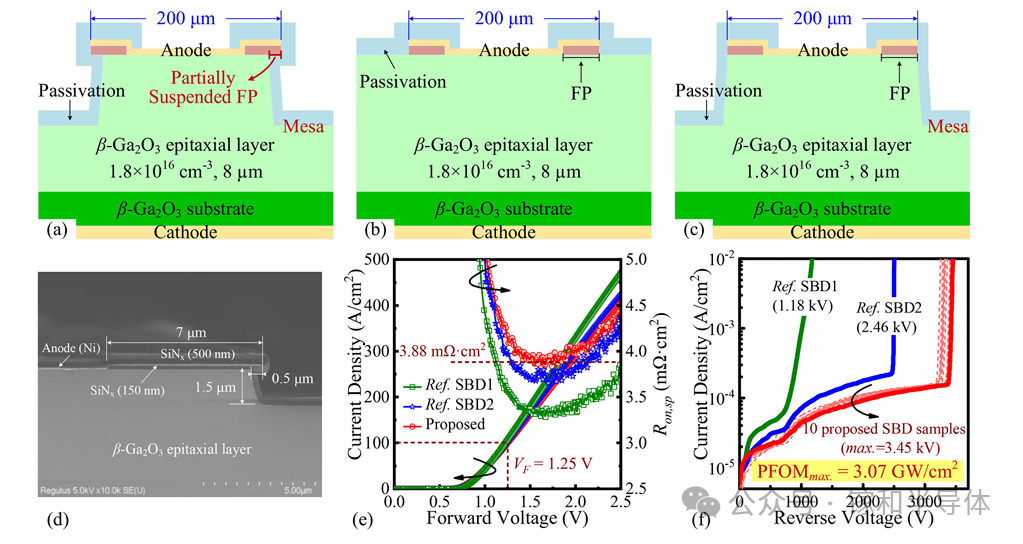
Figure 9. Device structure and electrical performance of β-Ga₂O₃ Schottky barrier diodes (SBDs) [23].
Summary of This Issue
β-Ga₂O₃ homoepitaxy is gradually transitioning from single-point performance breakthroughs toward engineering-scale development and large-scale manufacturing.
With its high growth rate, HVPE demonstrates clear advantages in the fabrication of thick drift layers and ten-kilovolt-class power devices. In contrast, MOCVD provides greater flexibility for the integrated growth of complex device structures and functional layers through precise control of doping concentration, layer thickness, and interface properties.
However, industrialization will ultimately not be determined by the highest growth rate or the narrowest XRD rocking curve achieved on an individual epitaxial sample. The key challenge lies in whether the technology can continuously and reliably deliver large-area wafers with low defect density, low impurity levels, uniform thickness, and controllable doping, and further translate these advantages into repeatable device performance and high manufacturing yield.
In the future, HVPE and MOCVD may no longer evolve as completely independent competing approaches. Instead, they are expected to form a more integrated ecosystem with substrate processing, chemical mechanical polishing (CMP), interface engineering, and device termination technologies.
Only when “high-efficiency thick-film growth” and “precise structural engineering” are effectively integrated can the key pathway for transforming β-Ga₂O₃ material advantages into commercial power-device applications be fully established.
Referance:
[1] APL Mater., 2025, 13: 100601.
[2] Jpn. J. Appl. Phys., 2017, 56: 110310.
[3] Sci. Technol. Adv. Mater., 2025, 26: 2585551.
[4] Semicond. Sci. Technol., 2023, 38: 105003.
[5] Appl. Phys. Lett., 2025, 126: 231605.
[6] Appl. Phys. Lett., 2022, 120: 102102.
[7] Appl. Phys. Express, 2015, 8: 015503.
[8] J. Cryst. Growth, 2014, 405: 19–22.
[9] Sci. Rep., 2020, 10: 22261.
[10] 人工晶体学报, 2025, 54(2): 227–232.
[11] J. Cryst. Growth, 2021, 564: 126129.
[12] Appl. Phys. Express, 2022, 15: 075503.
[13] Appl. Phys. Lett., 2023, 122: 162102.
[14] Jpn. J. Appl. Phys., 2023, 62: SF1021.
[15] APL Mater., 2023, 11: 111110.
[16] Nat. Commun., 2022, 13: 3900.
[17] ECS J. Solid State Sci. Technol., 2024, 13: 035003.
[18] AIP Adv., 2021, 11: 115323.
[19] Appl. Phys. Lett., 2024, 125: 242106.
[20] J. Vac. Sci. Technol. A, 2025, 43: 042702.
[21] Appl. Phys. Lett., 2023, 122: 232106.
[22] Phys. Rev. B, 2022, 105: 155201.
[23] Appl. Phys. Lett., 2025, 127: 092102.
Instruction
Official Account

Cooperation
Top
