


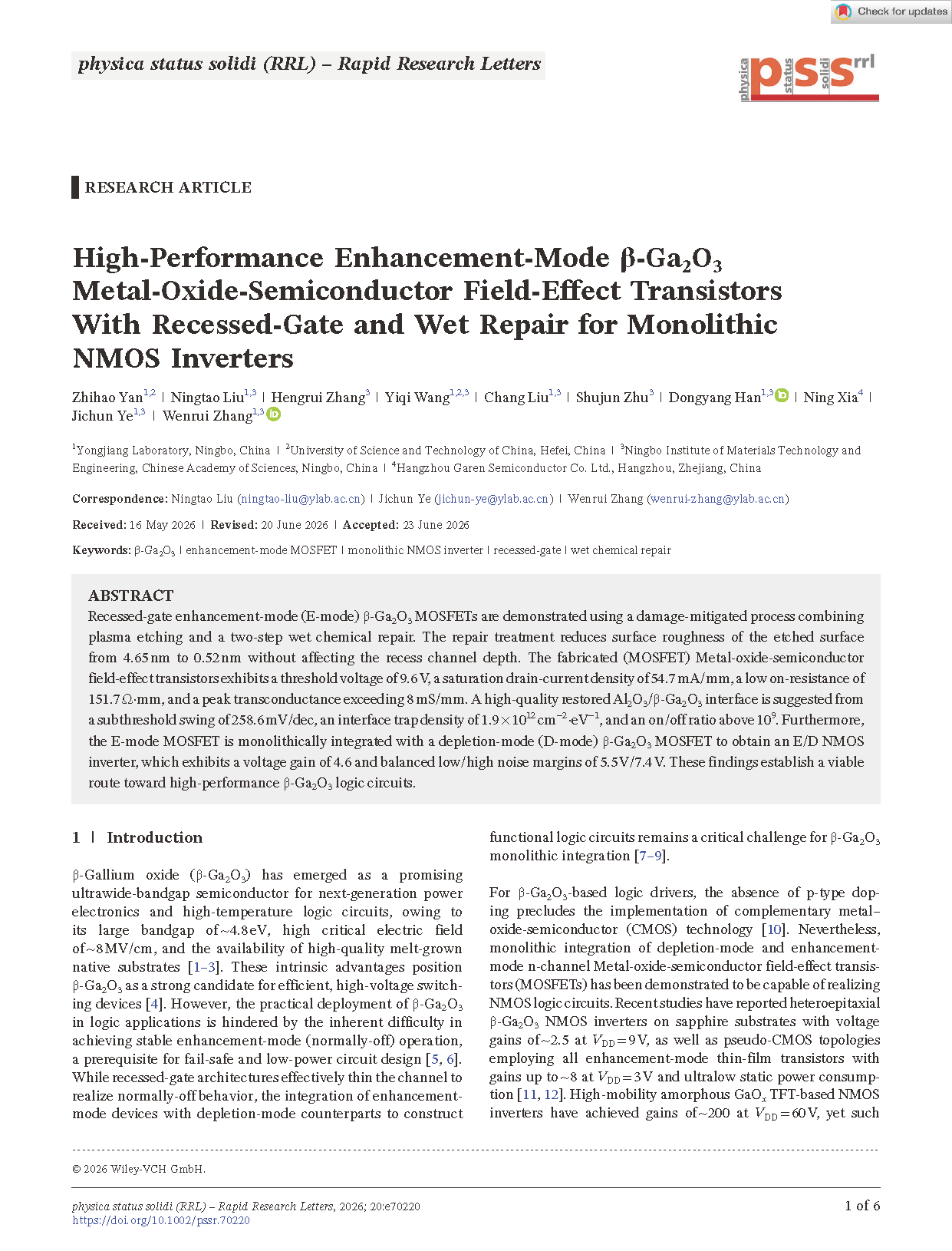
Researchers from Yongjiang Laboratory, University of Science and Technology of China, Ningbo Institute of Materials Technology and Engineering, Hangzhou Garen Semiconductor Co. Ltd. have published a paper titled "High-Performance Enhancement-Mode β-Ga₂O₃ Metal-Oxide-Semiconductor Field-Effect Transistors With Recessed-Gate and Wet Repair for Monolithic NMOS Inverters" in physica status solidi – Rapid Research Letters.
Background
β-Ga₂O₃ is an ultra-wide bandgap semiconductor with a bandgap of ~ 4.8 eV and a critical electric field of ~ 8 MV/cm. Melt-grown native substrates can be obtained, making it a core candidate for next-generation high-temperature logic and power devices. However, stable normally-off enhancement-mode operation is hard to realize, which restricts the development of fail-safe low-power logic circuits. Recessed-gate architecture thins the channel to achieve E-mode performance, while plasma etching introduces severe surface damage on β-Ga₂O₃, raising interface trap density and degrading gate control, on/off ratio and breakdown voltage.
Limited by poor channel interface quality after etching, previously reported β-Ga₂O₃ logic devices suffer low saturation current, poor subthreshold swing and insufficient breakdown voltage. CMOS circuits cannot be realized on β-Ga₂O₃, so logic inverters rely on monolithic integration of E/D-mode NMOS transistors. Existing inverters exhibit low voltage gain and unbalanced noise margins. In this work, a damage-mitigated recess-gate process combining plasma etching and two-step wet chemical repair is proposed to eliminate surface roughness and interfacial traps induced by etching. High-performance E-mode β-Ga₂O₃ MOSFETs are fabricated, and depletion-mode load transistors are integrated on the same epitaxial wafer to form NMOS inverters, providing a feasible manufacturing route for gallium oxide wide-bandgap logic integrated circuits.
Abstract
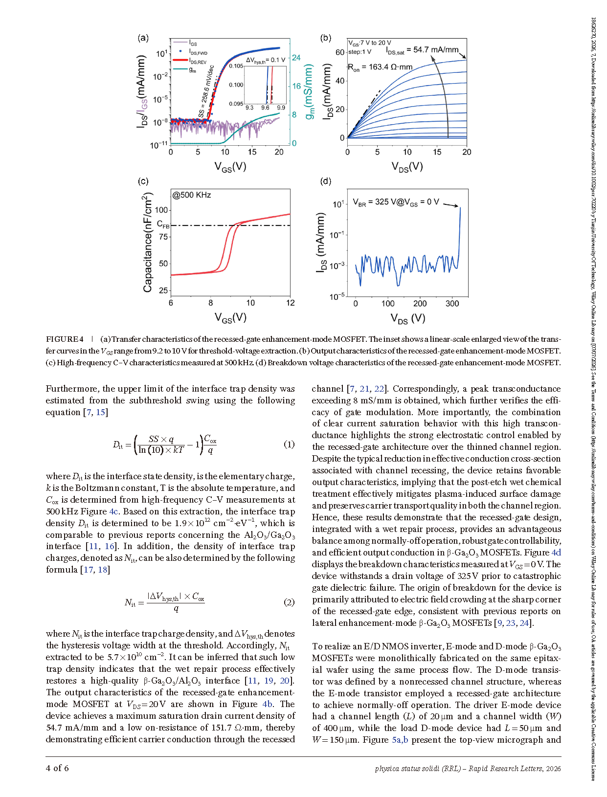
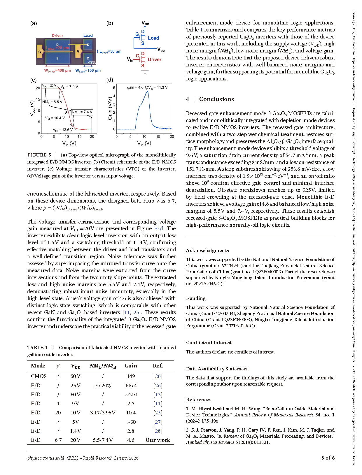
Recessed-gate enhancement-mode (E-mode) β-Ga₂O₃ MOSFETs are demonstrated using a damage-mitigated process combining plasma etching and a two-step wet chemical repair. The repair treatment reduces surface roughness of the etched surface from 4.65 nm to 0.52 nm without affecting the recess channel depth. The fabricated MOSFET exhibits a threshold voltage of 9.6 V, a saturation drain-current density of 54.7 mA/mm, a low on-resistance of 151.7 Ω·mm, and a peak transconductance exceeding 8 mS/mm. A high-quality restored Al₂O₃/β-Ga₂O₃ interface is suggested from a subthreshold swing of 258.6 mV/dec, an interface trap density of 1.9 × 10¹² cm⁻²·eV⁻¹, and an on/off ratio above 10⁹. Furthermore, the E-mode MOSFET is monolithically integrated with a depletion-mode (D-mode) β-Ga₂O₃ MOSFET to obtain an E/D NMOS inverter, which exhibits a voltage gain of 4.6 and balanced low/high noise margins of 5.5 V/7.4 V. These findings establish a viable route toward high-performance β-Ga₂O₃ logic circuits.
Highlights
A hybrid process of plasma etching + two-step wet repair is proposed to eliminate plasma-induced surface damage; the roughness decreases from 4.65 nm to 0.52 nm while the recess depth remains unchanged;
High-performance recessed-gate E-mode β-Ga₂O₃MOSFET is fabricated with on/off ratio over 10⁹ and low D_it of 1.9 × 10¹² cm⁻²·eV⁻¹, showing outstanding saturation current, transconductance and breakdown voltage;
Monolithic integration of E/D transistors on one wafer is realized to construct gallium oxide NMOS inverter with voltage gain of 4.6 and balanced noise margins;
The wet repair process requires no vacuum equipment and matches existing Ga₂O₃manufacturing lines, which reduces interface traps, suppresses hysteresis and strengthens electrostatic gate control;
The device achieves a breakdown voltage of 325 V, delivering high voltage and large current output compared with reported monolithic Ga₂O₃ logic devices.
Conclusion
Recessed-gate enhancement-mode β-Ga₂O₃ MOSFETs are fabricated and monolithically integrated with depletion-mode devices to realize E/D NMOS inverters. The recessed-gate architecture, combined with a two-step wet chemical treatment, restores surface morphology and preserves the Al₂O₃/β-Ga₂O₃ interface quality. The enhancement-mode device exhibits a threshold voltage of 9.6 V, a saturation drain current density of 54.7 mA/mm, a low on-resistance of 151.7 Ω·mm, and a peak transconductance exceeding 8 mS/mm. A steep subthreshold swing of 258.6 mV/dec, a low interface trap density of 1.9 × 10¹² cm⁻²·eV⁻¹, and an on/off ratio above 10⁹ confirm effective gate control and minimal interface degradation. Off-state breakdown reaches up to 325 V, limited by field crowding at the recessed-gate edge. Monolithic E/D inverters achieve a voltage gain of 4.6 and balanced low/high noise margins of 5.5 V and 7.4 V, respectively. These results establish recessed-gate β-Ga₂O₃ MOSFETs as practical building blocks for high-performance normally-off logic circuits.
Project Support
This work was supported by the National Natural Science Foundation of China (grant no. 62204244) and the Zhejiang Provincial Natural Science Foundation of China (grant no. LQ23F040003). Part of the research was supported by Ningbo Yongjiang Talent Introduction Programme (grant no. 2021A-046-C).
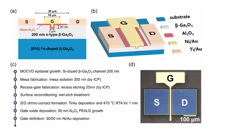
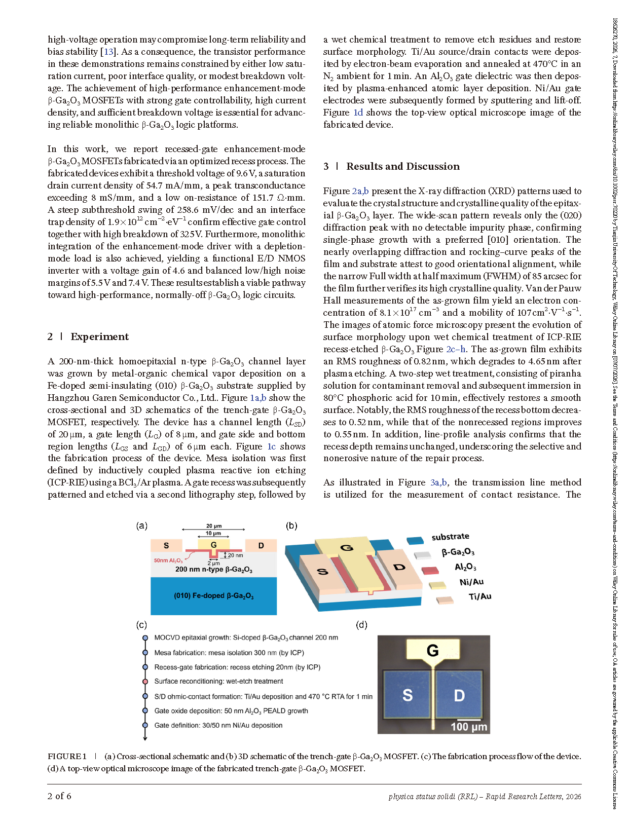
Figure 1 (a) Cross-sectional schematic of trench-gate β-Ga₂O₃ MOSFET; (b) 3D structural schematic of the device; (c) Full device fabrication flow chart; (d) Top-view optical micrograph of finished transistor
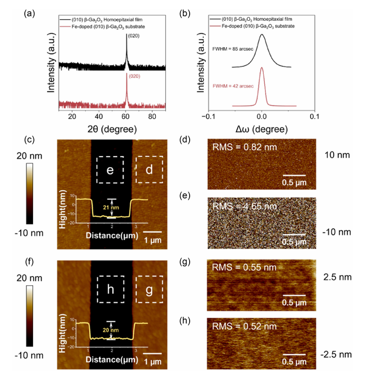
Figure 2 (a) XRD 2theta-omega scans of epitaxial film and substrate; (b) XRD rocking curves of (020) peak; AFM images of recess region before and after wet chemical repair
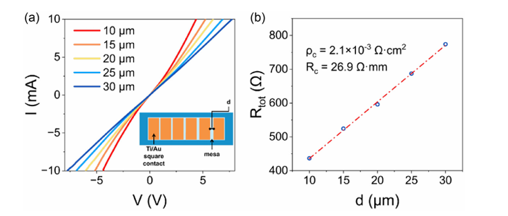
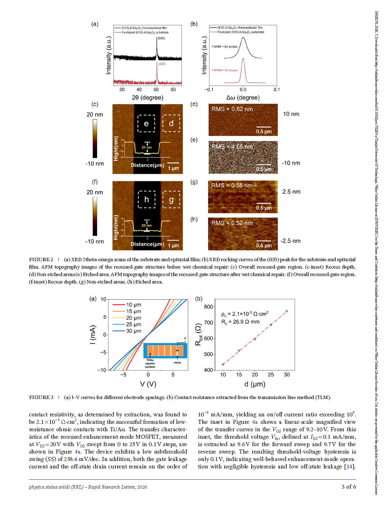
Figure 3 (a) I–V curves under different electrode spacings for TLM test; (b) Fitting curve of specific contact resistance extracted by transmission line method
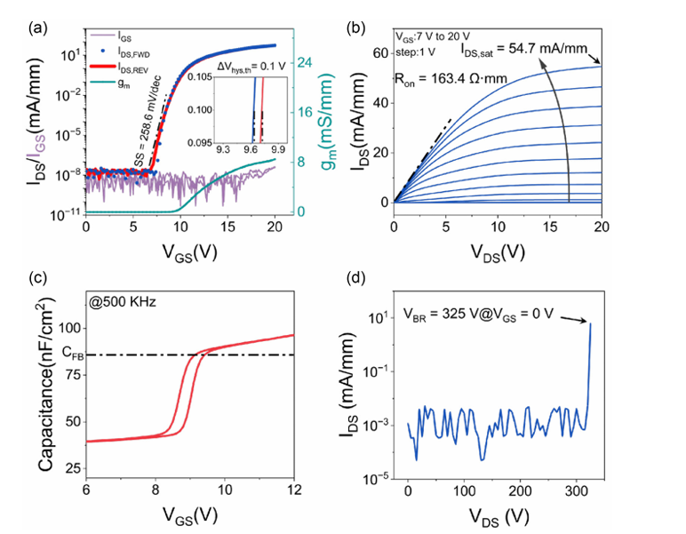
Figure 4 (a) Transfer characteristics with inset for threshold extraction; (b) Output characteristics; (c) High-frequency C–V curve at 500 kHz; (d) Off-state breakdown voltage curve
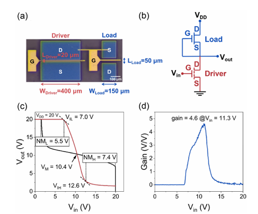
Figure 5 (a) Top-view micrograph of monolithic E/D NMOS inverter; (b) Circuit schematic; (c) Voltage transfer characteristic curve; (d) Voltage gain vs input voltage
DOI:
doi.org/10.1002/pssr.70220
Instruction
Official Account

Cooperation
Top
