



Researchers from Tianjin University, University College Dublin and The Hong Kong Microelectronics Research Institute have published a paper titled “Machine-learning-guided molecular dynamics simulations of point defect evolution in β-Ga₂O₃ during ion implantation and annealing” in Acta Materialia.
Background
Gallium oxide (Ga₂O₃) is an emerging ultrawide-bandgap semiconductor with a bandgap of approximately 4.8 eV and a theoretical breakdown electric field up to 8 MV/cm, which is promising for high-power electronics and solar-blind photodetectors. Among its five polymorphs, β-Ga₂O₃ owns the best thermodynamic stability and outstanding irradiation tolerance, since metastable γ-Ga₂O₃ can form under ion implantation to relieve lattice disorder. Ion implantation is a vital doping technique to tune the electrical properties of β-Ga₂O₃, yet it introduces massive point defects including interstitials and vacancies, and even triggers irreversible β-to-γ phase transition, deteriorating device performance severely. Conventional Wigner-Seitz (WS) defect analysis has obvious limitations for low-symmetry β-Ga₂O₃ crystal, and fails to accurately identify defects under thermal perturbation and high defect density. Most existing molecular dynamics (MD) simulations neglect electronic stopping effects, which overestimates ion range, defect concentration and temperature rise, making it hard to reveal atomic-scale defect evolution. In this work, a defect identification algorithm based on DBSCAN clustering and similarity matching is developed for β-Ga₂O₃. Combined with MD simulations incorporating electronic stopping, the evolution, recombination and phase transition mechanism of various point defects under multiple implantation fluences and annealing temperatures are systematically investigated, providing atomic-level theoretical guidance for ion implantation process optimization.
Abstract
In beta-gallium oxide (β-Ga₂O₃), Ga-ion implantation and subsequent annealing induce abundant point defects, including interstitials and vacancies. To overcome the limitations of conventional Wigner-Seitz (WS) defect analysis, a defect identification algorithm based on similarity matching and spatial clustering via density-based spatial clustering of applications with noise (DBSCAN) is developed specifically for β-Ga₂O₃. This algorithm accurately distinguishes lattice atoms from point defects under thermal perturbations and at high defect concentrations, and further identifies eight configurations of Ga interstitials (Gaᵢₐ to Gaᵢₕ) by analyzing atomic coordination environments. Simulations comparing Stopping and Range of Ions in Matter (SRIM) and molecular dynamics (MD) data, along with single-ion implantation analysis, highlight the significance of electronic stopping effects: neglecting electronic stopping leads to overestimated ion range, defect concentration, and temperature rise. Across five implantation fluences (1 to 5×10¹⁴ cm⁻²) and corresponding annealing processes, 1373 K is identified as the optimal recovery temperature. Multiscale analyses based on hydrostatic stress, partial radial distribution function (PRDF), and defect concentration reveal the evolution and spatial distribution of point defects. The results demonstrate that Ga interstitials (Gaᵢ) tend to occupy tetrahedral and octahedral interstitial sites, and the accumulation and recombination of point defects drive a defect-mediated phase transition from β- to γ-Ga₂O₃. With increasing fluences followed by annealing, β-phase recovery declines while γ-phase transformation rises, leading to an irreversible phase transition. In contrast, the migration of oxygen interstitials (Oᵢ) is more sensitive to annealing temperature, and appropriate annealing temperature significantly enhances recrystallization of the O-sublattice.
Highlights
A DBSCAN clustering and similarity-matching defect recognition algorithm is proposed for low-symmetry β-Ga₂O₃ lattices, eliminating the errors of traditional WS method and realizing identification of eight Ga interstitial configurations and five vacancy types;
Comparison between SRIM and MD simulations verifies the indispensable electronic stopping effect, whose absence severely overestimates ion penetration depth, defect density and collision-induced temperature rise;
Simulations of five implantation fluences ranging from 1 to 5×10¹⁴ cm⁻² confirm 1373 K as the optimal annealing temperature; insufficient recovery occurs at low temperature while surface amorphization defects form at excessive high temperature;
It is clarified that Gaᵢ atoms occupy tetrahedral and octahedral interstitial sites and form complex defects with Ga vacancies, triggering irreversible β-to-γ phase transition, while O sublattice can recover more easily under thermal treatment;
Partial radial distribution function and hydrostatic stress field are adopted to analyze defect distribution, revealing the atomic-scale intrinsic mechanism of fluence-dependent phase transformation.
Conclusion
In this study, a similarity-matching algorithm based on DBSCAN clustering was developed. This method effectively distinguishes point defects (interstitials and vacancies) from lattice atoms, enabling accurate identification even under thermal perturbations and at high defect densities. Subsequently, by comparing SRIM simulations with MD simulations and performing single-ion implantation in MD, the influence of electronic stopping on the ion range was investigated. It was found that neglecting electronic stopping significantly overestimates the ion range, system temperature, and the concentrations of various defects. Using MD simulations, a comprehensive atomic-scale analysis of the defect evolution mechanism during Ga ion implantation and subsequent annealing in β-Ga₂O₃ was performed. The results reveal that Gaᵢ tends to occupy eight interstitial sites (from Gaᵢₐ to Gaᵢₕ) during implantation and annealing, forming complex structures with adjacent VGa that introduce tensile stress. These interstitial configurations are identified as the primary factors inducing the β-to-γ phase transition in β-Ga₂O₃. Furthermore, the migration behavior of Gaᵢ shows that with increasing fluences, the tendency for the γ-phase transformation in post-annealed β-Ga₂O₃ rises continuously, accompanied by a corresponding decrease in the trend of β-phase recovery, ultimately leading to an irreversible phase transition. In contrast, Oᵢ exhibits temperature-dependent migration behavior, and the O-sublattice demonstrates relatively high rigidity.
Project Support
This work was supported by the National Key Research and Development Program Project (2024YFF0726104).
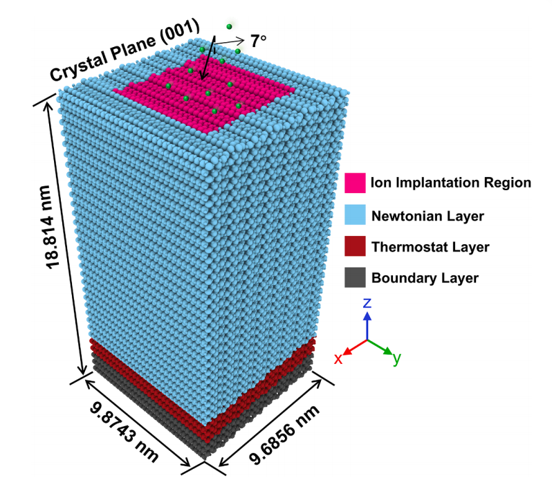
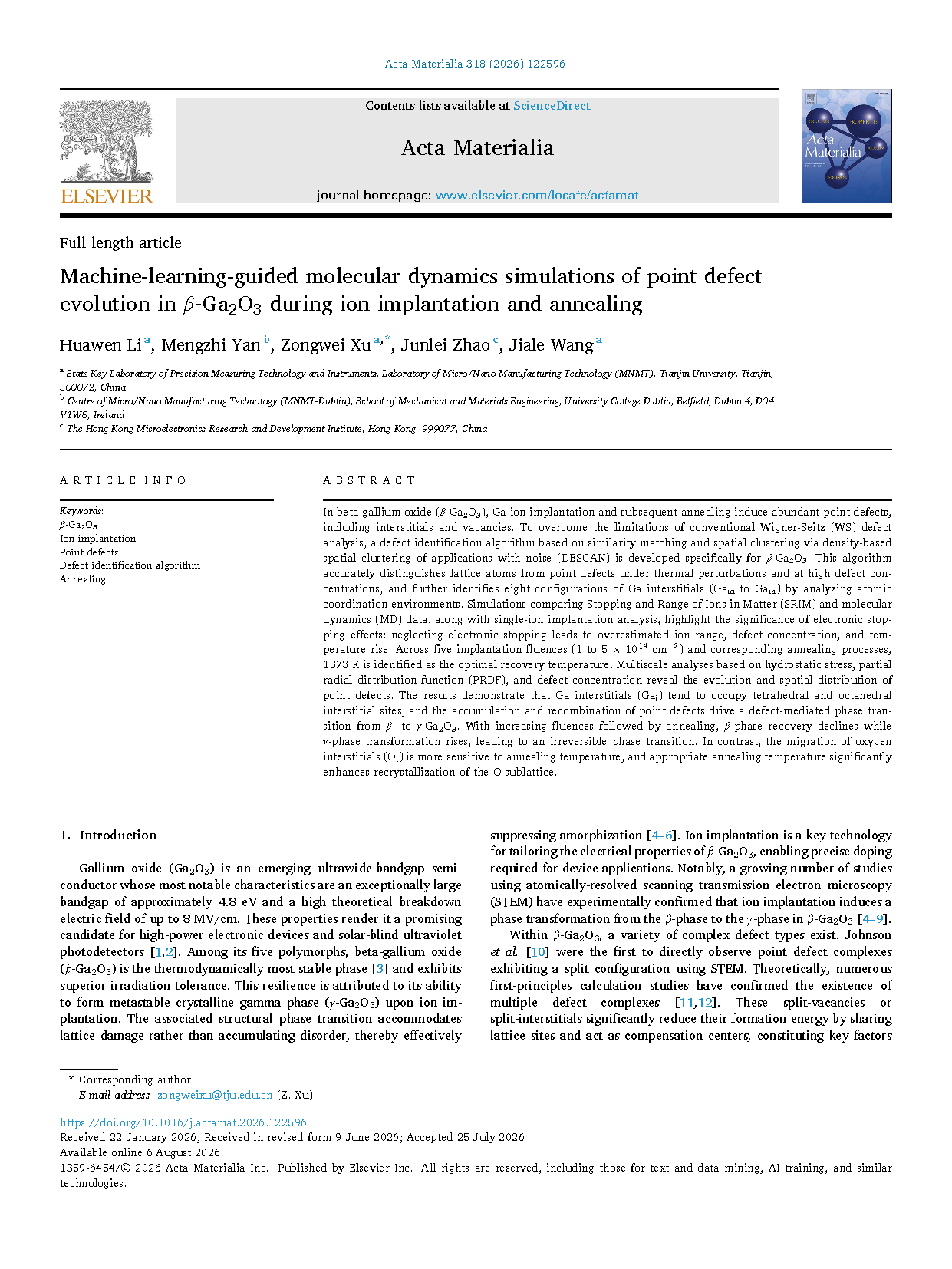
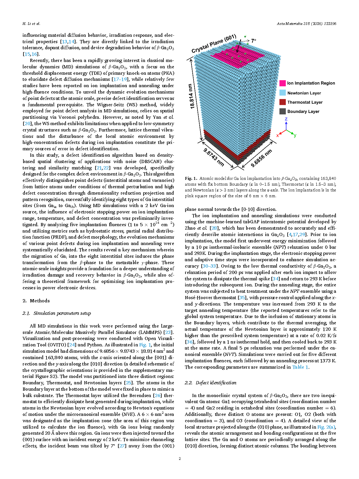
Figure 1. Atomic model for Ga ion implantation into β-Ga₂O₃, containing 163,840 atoms with fix bottom Boundary (z in 0-1.5 nm), Thermostat (z in 1.5-3 nm), and Newtonian (z>3 nm) layers along the Z-axis. The ion implantation is in the pink square region of the size of 6 nm×6 nm.
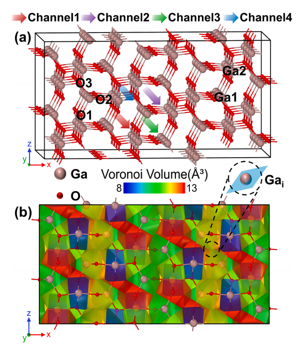
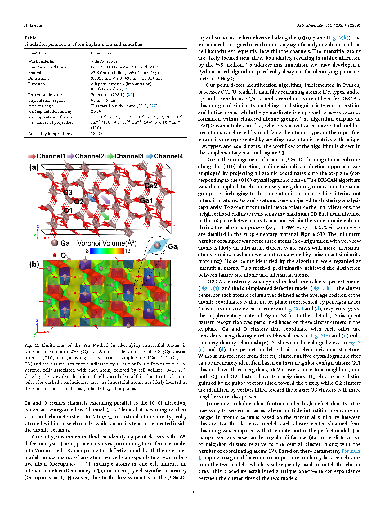
Figure 2. Limitations of the WS Method in Identifying Interstitial Atoms in Non centrosymmetric β-Ga₂O₃. (a) Atomic-scale structure of β-Ga₂O₃ viewed from the (010) plane, showing the five crystallographic sites (Ga1, Ga2, O1, O2, O3) and the channel structures indicated by arrows of four different colors. (b) Voronoi cells associated with each atom, colored by cell volume (8-13 ų), showing the prevalent location of cell boundaries within the structural channels. The dashed box indicates that the interstitial atoms are likely located at the Voronoi cell boundaries (indicated by blue planes).
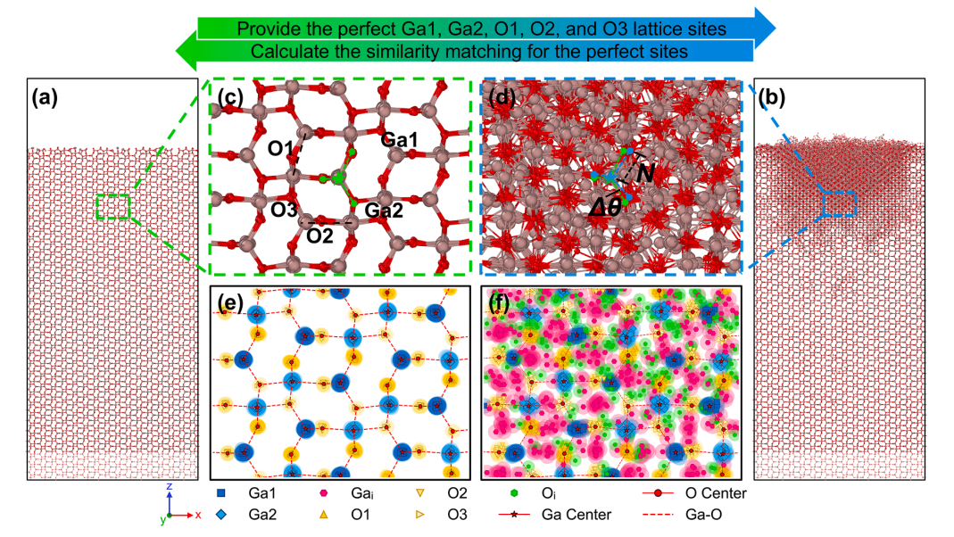
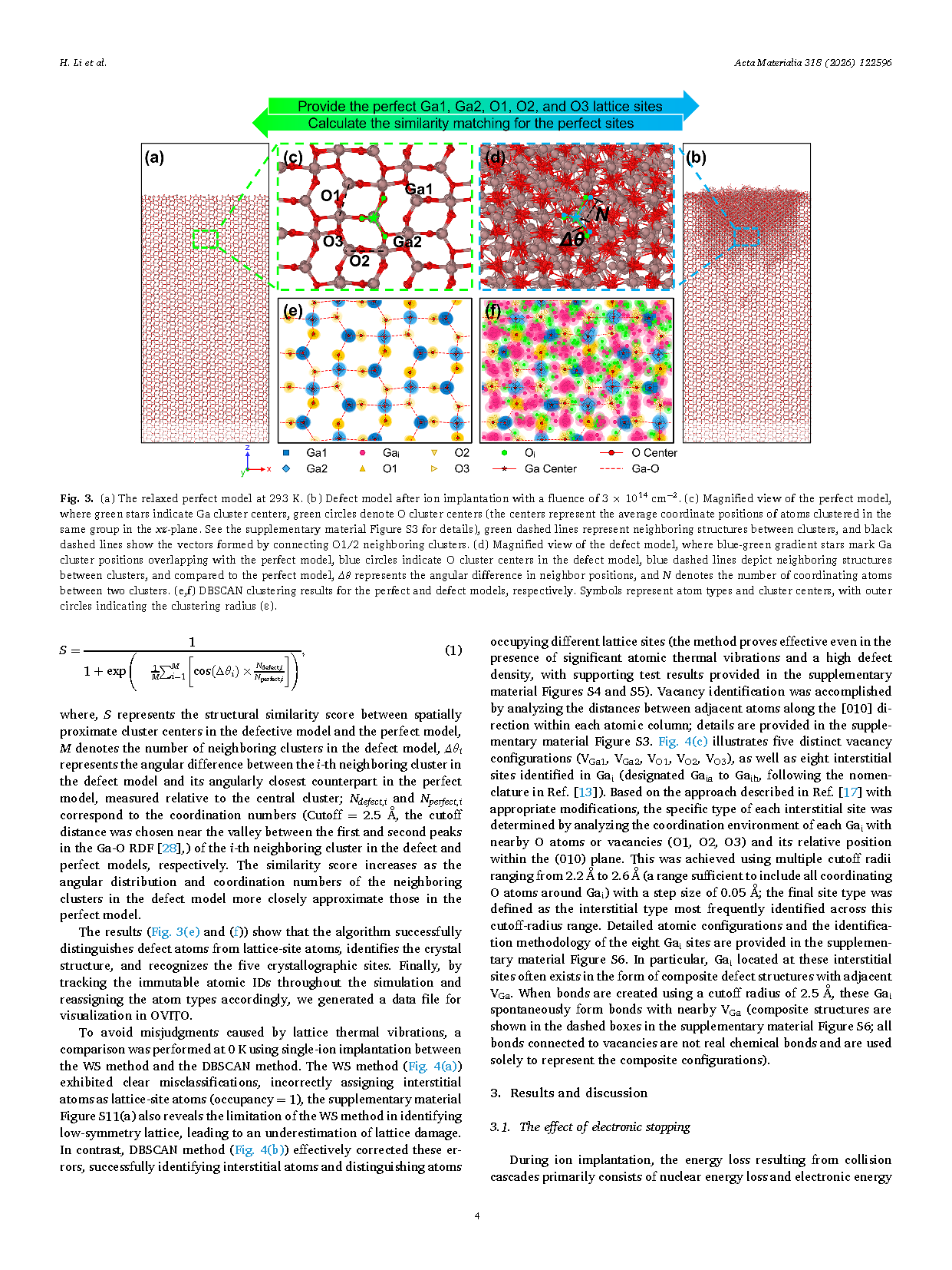
Figure 3. (a) The relaxed perfect model at 293 K. (b) Defect model after ion implantation with a fluence of 3×10¹⁴ cm⁻². (c) Magnified view of the perfect model, where green stars indicate Ga cluster centers, green circles denote O cluster centers (the centers represent the average coordinate positions of atoms clustered in the same group in the xz-plane. See the supplementary material Figure S3 for details), green dashed lines represent neighboring structures between clusters, and black dashed lines show the vectors formed by connecting O1/2 neighboring clusters. (d) Magnified view of the defect model, where blue-green gradient stars mark Ga cluster positions overlapping with the perfect model, blue circles indicate O cluster centers in the defect model, blue dashed lines depict neighboring structures between clusters, and compared to the perfect model, Δθ represents the angular difference in neighbor positions, and N denotes the number of coordinating atoms between two clusters. (e,f) DBSCAN clustering results for the perfect and defect models, respectively. Symbols represent atom types and cluster centers, with outer circles indicating the clustering radius (ε).
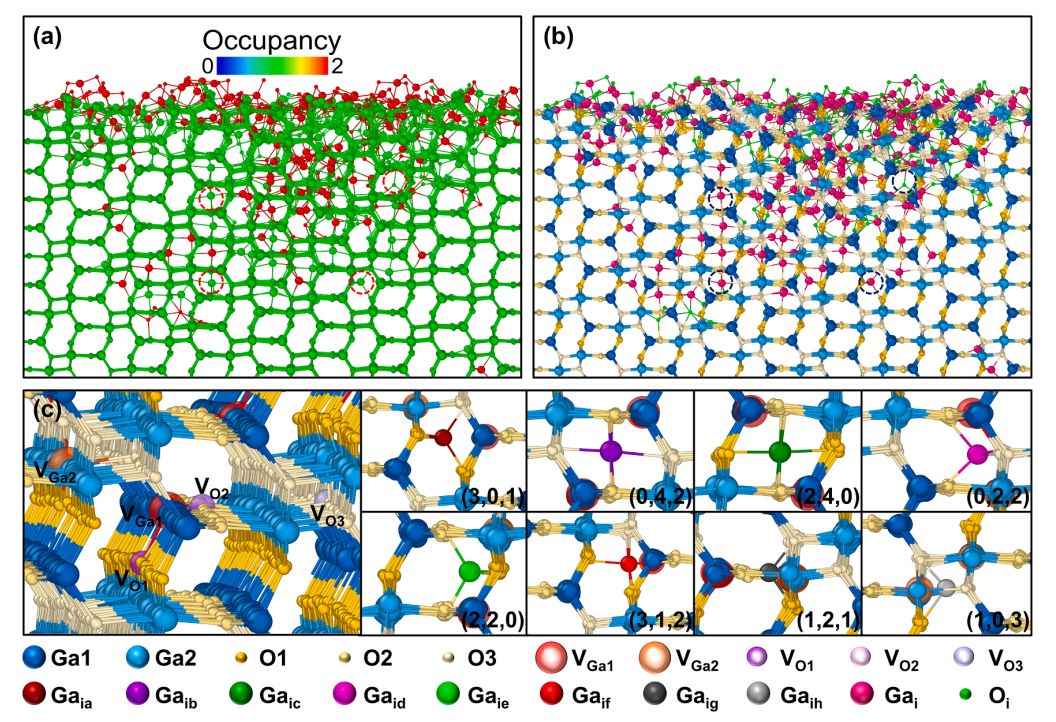
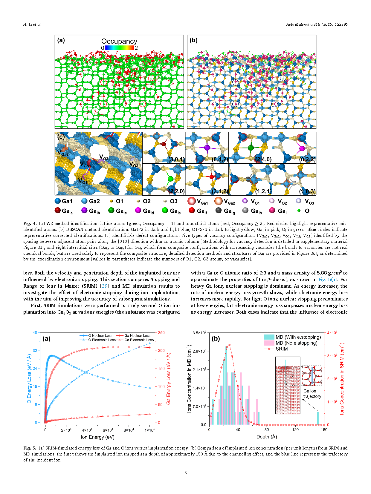
Figure 4. (a) WS method identification: lattice atoms (green, Occupancy =1) and interstitial atoms (red, Occupancy ≥ 2). Red circles highlight representative misidentified atoms. (b) DBSCAN method identification: Ga1/2 in dark and light blue; O1/2/3 in dark to light yellow; Gaᵢ in pink; Oᵢ in green. Blue circles indicate representative corrected identifications. (c) Identifiable defect configurations: Five types of vacancy configurations (VGa1, VGa2, VO1, VO2, VO3), and eight interstitial sites (Gaₐ to Gaₕ) for Gaᵢ, which form composite configurations with surrounding vacancies (the bonds to vacancies are not real chemical bonds, but are used solely to represent the composite structure; detailed detection methods and structures of Gaᵢ are provided in supplementary Figure S6), as determined by the coordination environment (values in parentheses indicate the numbers of O1, O2, O3 atoms).
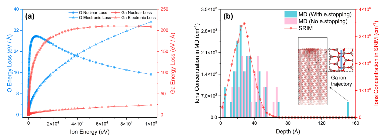
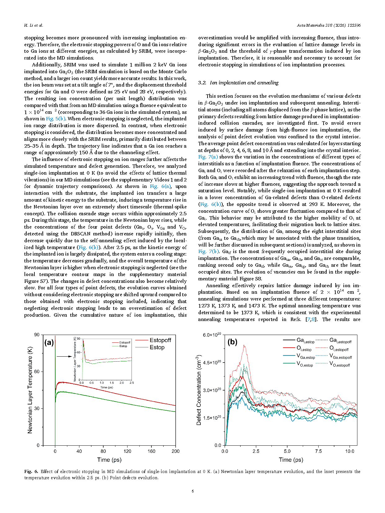
Figure 5. (a) SRIM-simulated energy loss of Ga and O ions versus implantation energy. (b) Comparison of implanted ion concentration (per unit length) from SRIM and MD simulations, the inset shows the implanted ion trapped at a depth of approximately 150 Å due to the channeling effect, and the blue line represents the trajectory of the incident ion.
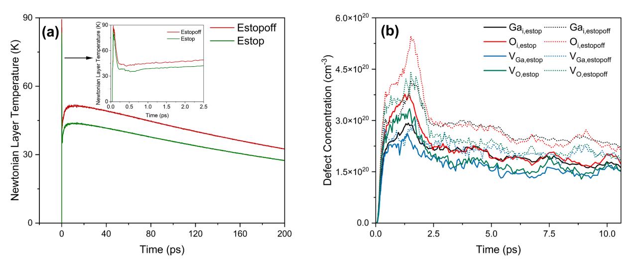
Figure 6. Effect of electronic stopping in MD simulations of single-ion implantation at 0 K. (a) Newtonian layer temperature evolution, and the inset presents the temperature evolution within 2.5 ps. (b) point defects evolution.
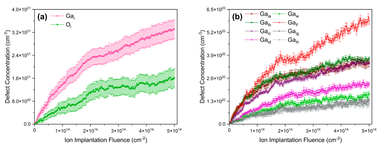
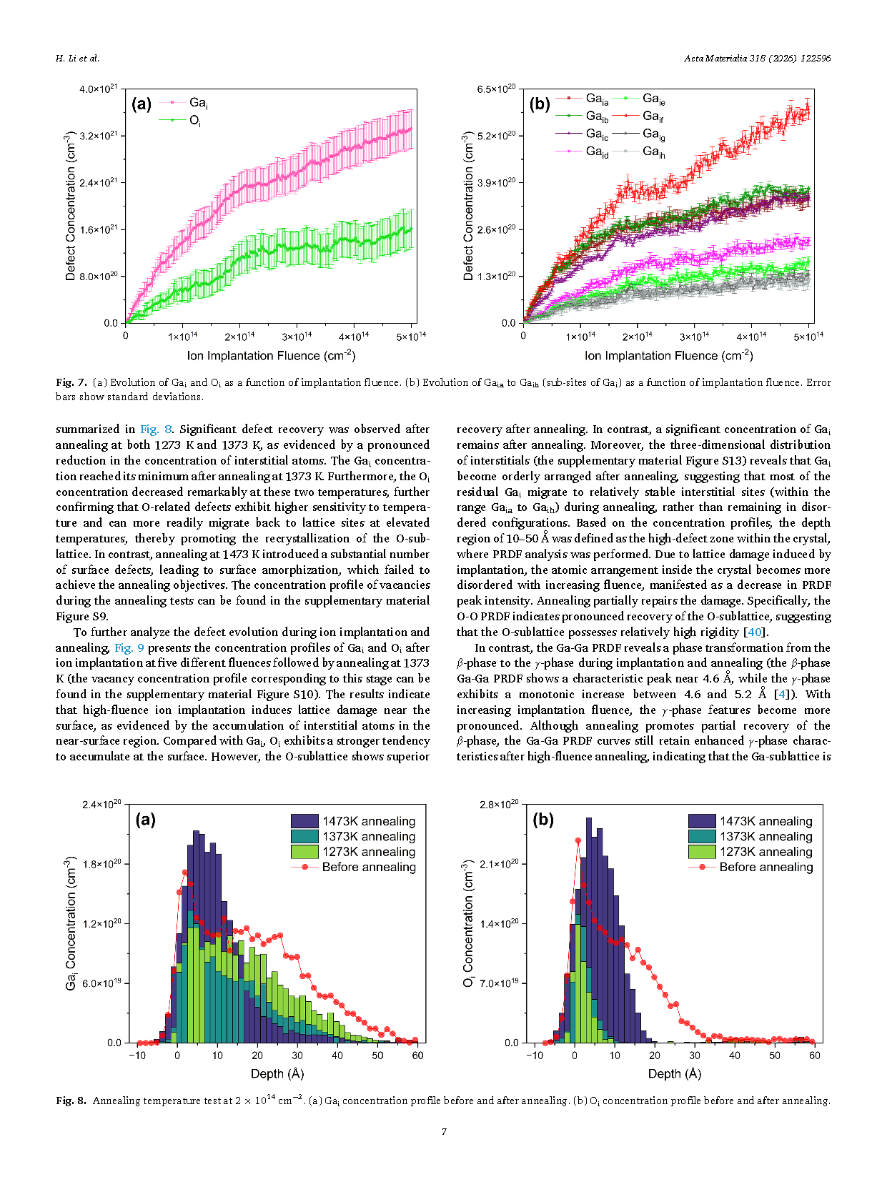
Figure 7. (a) Evolution of Gaᵢ and Oᵢ as a function of implantation fluence. (b) Evolution of Gaᵢₐ to Gaᵢₕ (sub-sites of Gaᵢ) as a function of implantation fluence. Error bars show standard deviations.
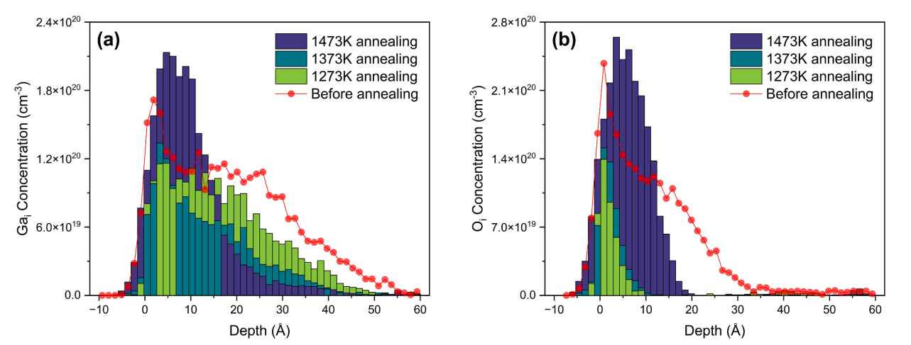
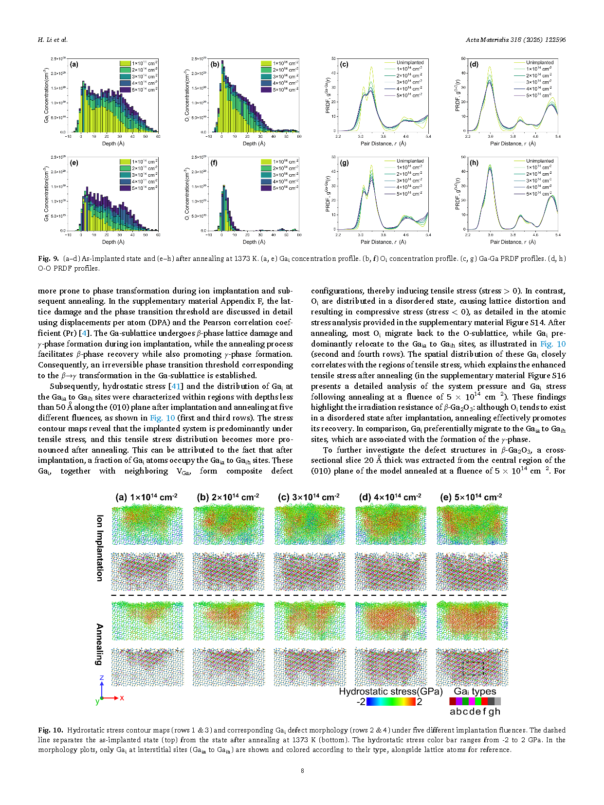
Figure 8. Annealing temperature test at 2×10¹⁴ cm⁻². (a) Gaᵢ concentration profile before and after annealing. (b) Oᵢ concentration profile before and after annealing.
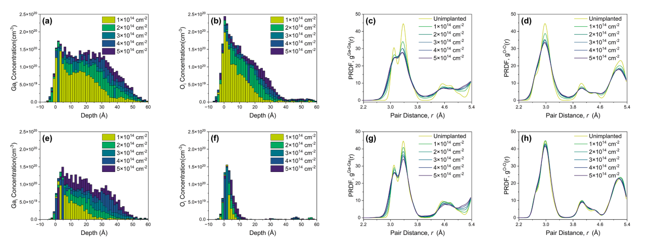
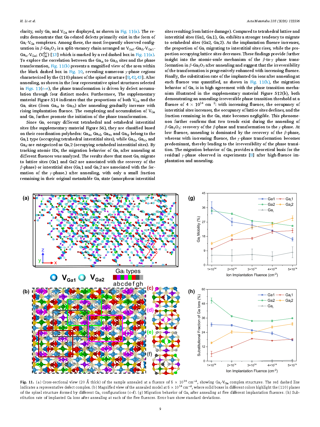
Figure 9. (a-d) As-implanted state and (e-h) after annealing at 1373 K. (a, e) Gaᵢ concentration profile. (b, f) Oᵢ concentration profile. (c, g) Ga-Ga PRDF profiles. (d, h) O-O PRDF profiles.
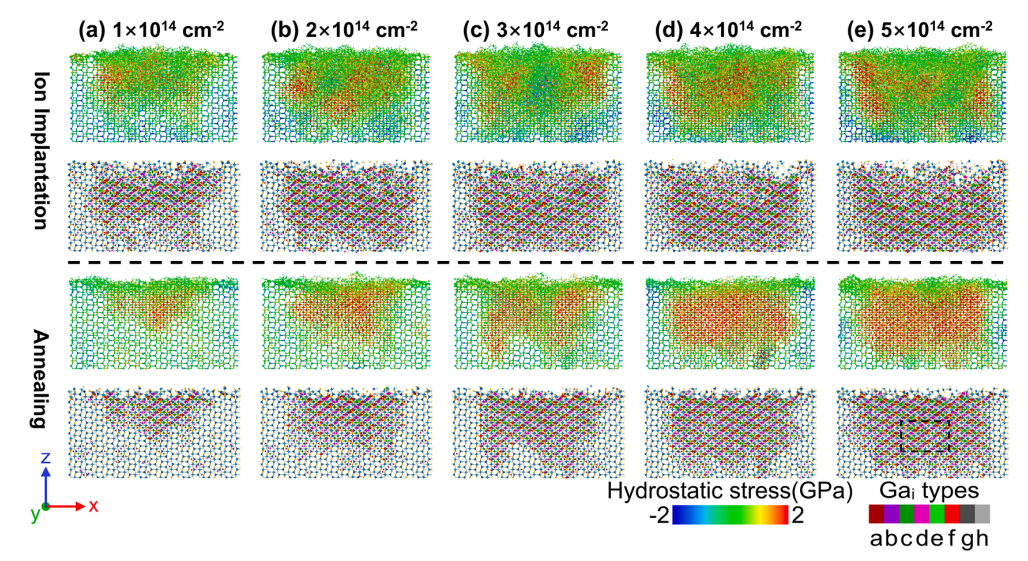
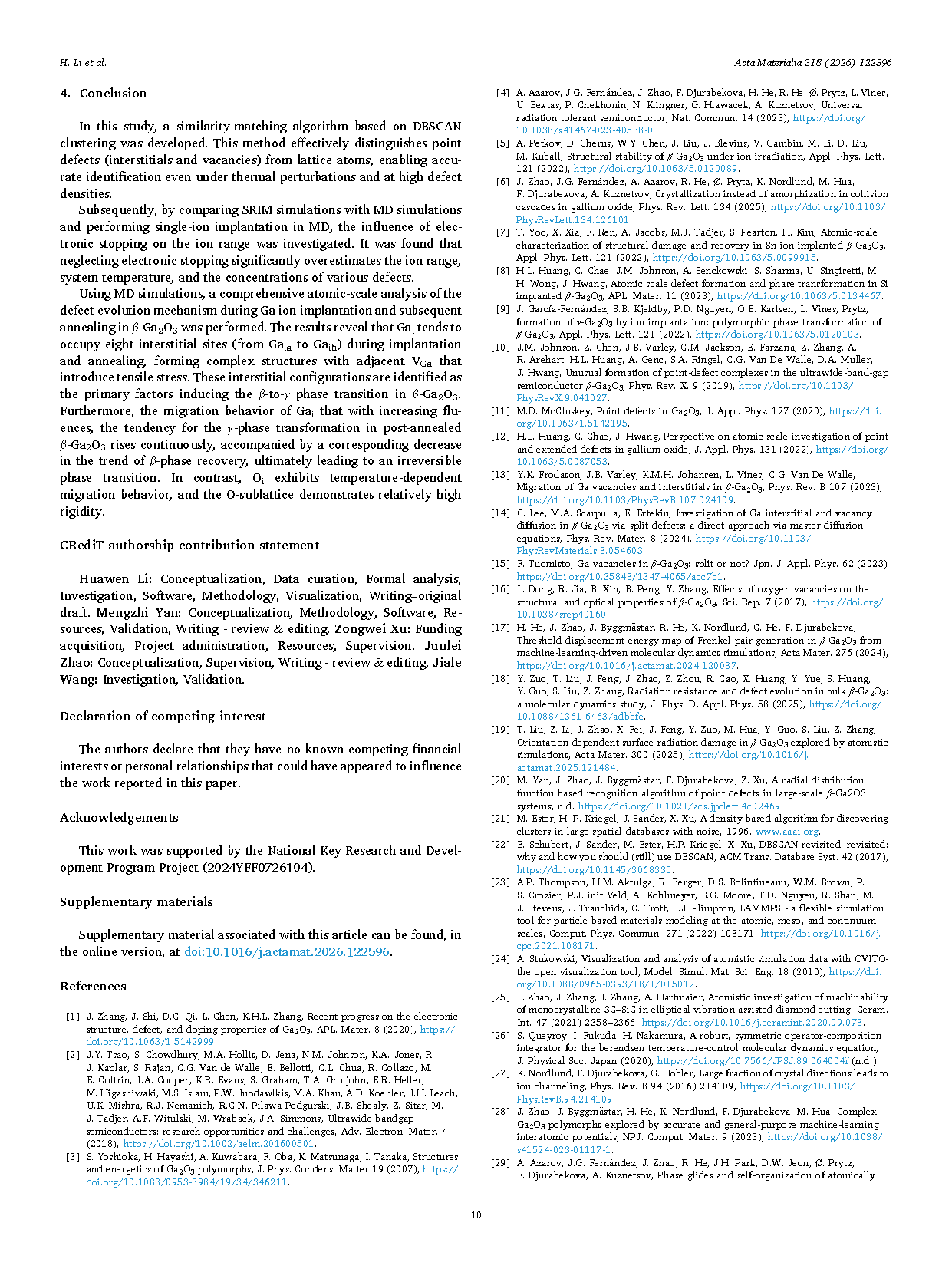
Figure 10. Hydrostatic stress contour maps (rows 1 & 3) and corresponding Gaᵢ type defect morphology (rows 2 & 4) under five different implantation fluences. The dashed line separates the as-implanted state from the state after annealing at 1373 K. In the morphology plots, only Gaᵢ at interstitial sites (Gaᵢₐ to Gaᵢₕ) are shown and colored according to their type, alongside lattice atoms for reference. The hydrostatic stress color bar ranges from -2 to 2 GPa.
DOI:
doi.org/10.1016/j.actamat.2026.122596
Instruction
Official Account

Cooperation
Top
