


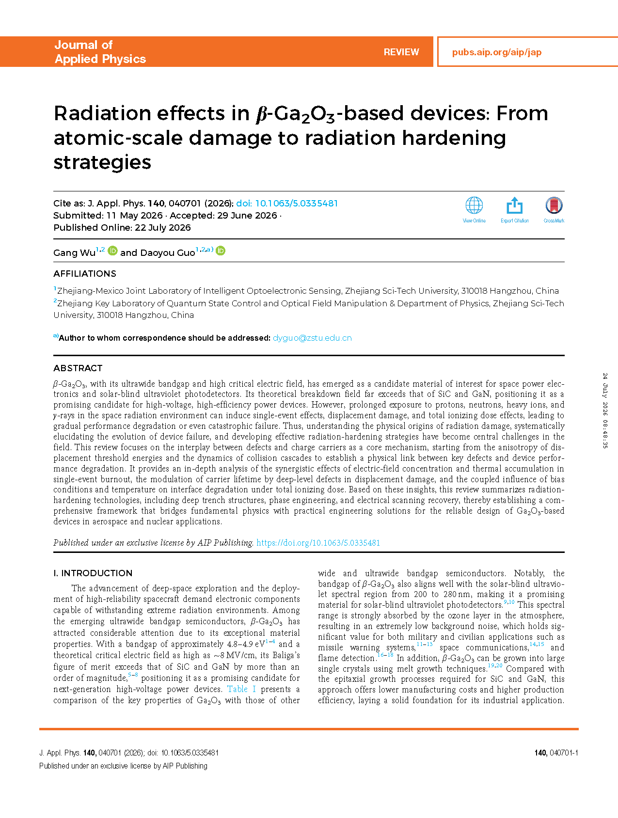
Researchers from the Zhejiang Sci-Tech University have published a dissertation titled " Radiation effects in β-Ga₂O₃-based devices: From atomic-scale damage to radiation hardening strategies " in Journal of Applied Physics.
Background
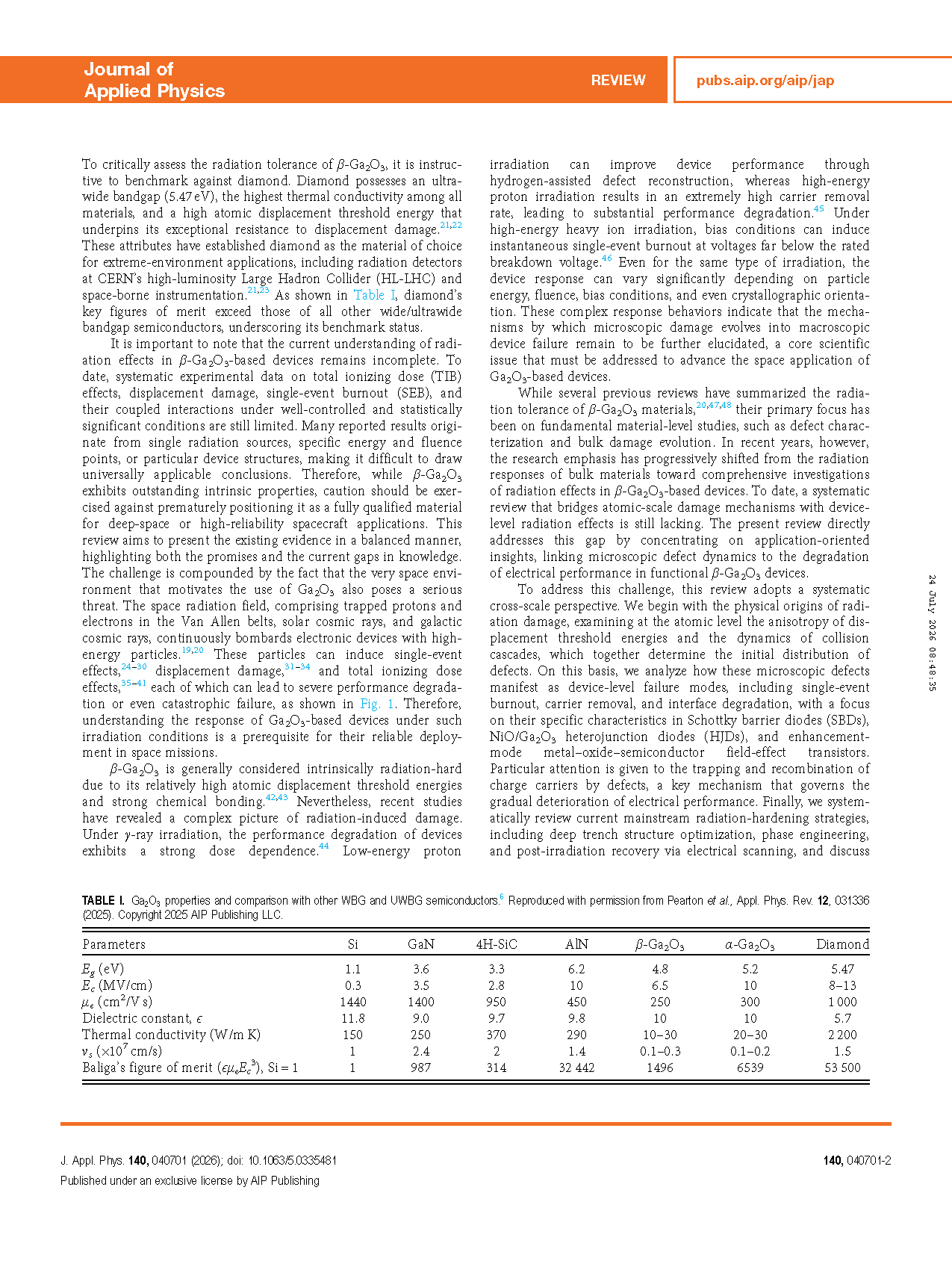
With the rapid advancement of deep-space exploration and high-reliability spacecraft deployment, electronic components that can withstand extreme space radiation environments are urgently required. Ultra-wide bandgap semiconductors are core candidate materials for aerospace power devices and solar-blind ultraviolet photodetectors. Among them, β-Ga₂O₃ possesses an ultra-wide bandgap of 4.8–4.9 eV and a theoretical critical electric field up to 8 MV/cm, whose Baliga’s figure of merit is far superior to SiC and GaN. Moreover, large-size single crystals of β-Ga₂O₃ can be fabricated via melt growth methods with lower manufacturing costs, enabling dual applications in high-voltage power electronics and 200–280 nm solar-blind ultraviolet detection for military missile warning, space communication and civilian flame monitoring.
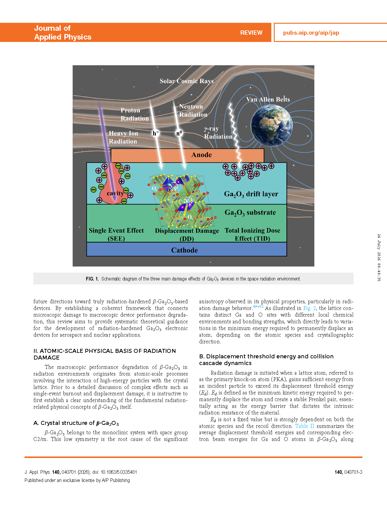
Nevertheless, the complex space radiation environment consisting of Van Allen belt trapped particles, solar cosmic rays and galactic cosmic rays continuously bombards β-Ga₂O₃ devices with high-energy protons, neutrons, heavy ions and γ-rays, triggering three dominant degradation modes: single-event effects, displacement damage and total ionizing dose effects. High-energy particles collide with crystal lattices to generate Frenkel pairs and deep-level traps, which capture charge carriers persistently and lead to carrier removal and increased on-resistance; heavy ions induce localized intense ionization, transient high current and Joule heat accumulation, further resulting in catastrophic single-event burnout; long-term cumulative ionization deteriorates semiconductor/dielectric interfaces, causing elevated leakage current and reduced breakdown voltage.
Existing research on radiation damage of β-Ga₂O₃ mainly focuses on bulk material intrinsic defect characterization, lacking systematic reviews bridging atomic-scale lattice damage and cross-scale electrical/optical device degradation. Most reported irradiation experiments adopt single radiation source with fixed energy and fluence, and there is no unified theoretical framework to explain synergistic damage coupled with crystal orientation, electrical bias and temperature. In addition, mainstream radiation hardening strategies including deep trench design, phase engineering and electrical scanning recovery have not been comprehensively summarized, hindering the practical deployment of β-Ga₂O₃ devices in aerospace and nuclear industries. This review therefore establishes a cross-scale systematic framework to connect fundamental atomic physics with engineering-oriented radiation-hardened device design.
Abstract
β-Ga₂O₃, with its ultrawide bandgap and high critical electric field, has emerged as a candidate material of interest for space power electronics and solar-blind ultraviolet photodetectors. Its theoretical breakdown field far exceeds that of SiC and GaN, positioning it as a promising candidate for high-voltage, high-efficiency power devices. However, prolonged exposure to protons, neutrons, heavy ions, and γ-rays in the space radiation environment can induce single-event effects, displacement damage, and total ionizing dose effects, leading to gradual performance degradation or even catastrophic failure. Thus, understanding the physical origins of radiation damage, systematically elucidating the evolution of device failure, and developing effective radiation-hardening strategies have become central challenges in the field. This review focuses on the interplay between defects and charge carriers as a core mechanism, starting from the anisotropy of displacement threshold energies and the dynamics of collision cascades to establish a physical link between key defects and device performance degradation. It provides an in-depth analysis of the synergistic effects of electric-field concentration and thermal accumulation in single-event burnout, the modulation of carrier lifetime by deep-level defects in displacement damage, and the coupled influence of bias conditions and temperature on interface degradation under total ionizing dose. Based on these insights, this review summarizes radiation-hardening technologies, including deep trench structures, phase engineering, and electrical scanning recovery, thereby establishing a comprehensive framework that bridges fundamental physics with practical engineering solutions for the reliable design of Ga₂O₃-based devices in aerospace and nuclear applications.
Highlights
A full cross-scale framework is constructed to connect atomic-scale lattice damage, device-level radiation-induced failure and engineering radiation-hardening strategies, overcoming the limitation of previous reviews only focusing on bulk material defects without device degradation correlation.
Differentiated single-event burnout mechanisms of three mainstream β-Ga₂O₃ power devices (SBD, NiO/Ga₂O₃ HJD, enhancement-mode MOSFET) are elaborated, and direct/indirect SEB triggering paths induced by heavy ions, protons and neutrons are distinguished.
Distinct damage evolution rules of four typical radiation sources (protons, neutrons, electrons, γ-rays) are systematically summarized, including the dual effect of low-energy proton repairing/high-energy proton degradation, neutron-induced lattice amorphization, electron-generated simple Frenkel pairs and γ-ray irradiation annealing effect coupled with electrical bias; a complete comparison database of carrier removal rates and defect energy levels is established.
Synergistic modulation effects of crystal orientation, working bias and ambient temperature on radiation defect generation, diffusion and recombination are clarified, revealing the atomic origin of radiation tolerance discrepancy between (010) and (−201) substrate devices.
Three categories of implementable radiation-hardening technologies are comprehensively reviewed: deep trench structure design for transient hole dissipation, intrinsic radiation resistance modification via polymorph engineering/doping/crystal plane selection, and post-irradiation electrical scanning low-temperature recovery; diamond/Ga₂O₃ hybrid ultra-wide bandgap heterostructure is proposed as a promising route for next-generation ultra-radiation-hardened devices.
Conclusion
This review has systematically consolidated the response behavior of β-Ga₂O₃-based power and optoelectronic devices under complex radiation environments, constructing a cross-scale knowledge framework that spans from atomic-scale damage mechanisms to macroscopic device performance degradation and, ultimately, to radiation-hardening strategies. At the atomic scale, the review established that the anisotropy of displacement threshold energies constitutes the physical foundation for understanding radiation damage in β-Ga₂O₃. The various types of radiation-induced point defects and their energy level positions were systematically summarized, identifying the gallium vacancy-related E2* trap as the key defect responsible for carrier removal and performance degradation. At the device level, the review provided an in-depth analysis of failure mechanisms under different radiation effects. For single-event effects, localized intense ionization and Joule heating triggered by heavy ion incidence were identified as the root causes of burnout in both Schottky barrier diodes and heterojunction diodes, with burnout sites closely correlated with electric-field distribution. Displacement damage and total ionizing dose effects progressively degrade device electrical characteristics through the cumulative introduction of deep-level defects. However, under specific conditions such as low-energy proton or γ-ray irradiation, performance improvements attributed to hydrogen passivation or irradiation annealing effects have also been observed. Furthermore, the review explored the multidimensional impact of radiation on heterojunction interfaces, dielectric layers, and the optical and thermal properties of the material, revealing the complexity of radiation damage. Finally, current mainstream radiation-hardening technologies were summarized, including the dissipation of transient holes generated by single-event effects through optimized device structures, and post-irradiation performance recovery utilizing electrical scanning or low-temperature annealing. These findings provide important references for enhancing the reliability of β-Ga₂O₃ devices in space environments.
Project Support
This work was supported by the National Natural Science Foundation of China (Nos. U23A20349, 62274148, and 62374147) and the Natural Science Foundation of Hangzhou (No. 2024SZRZDF040001).
FIG. 1 Schematic diagram of the three main damage effects of Ga₂O₃ devices in the space radiation environment.
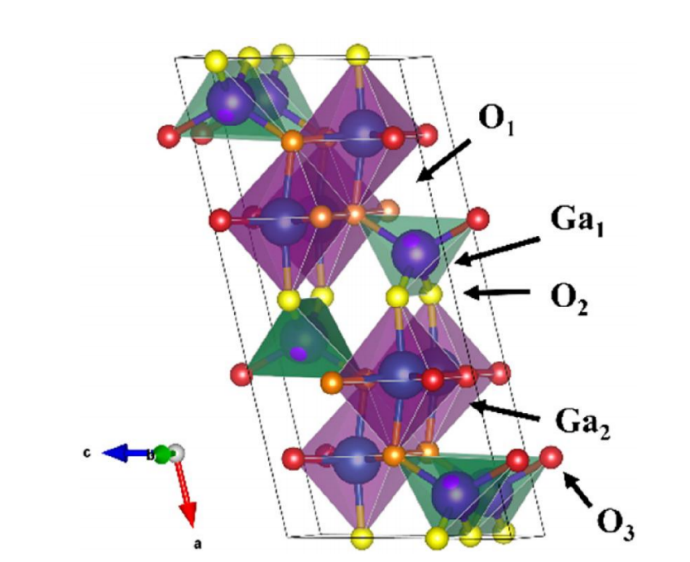
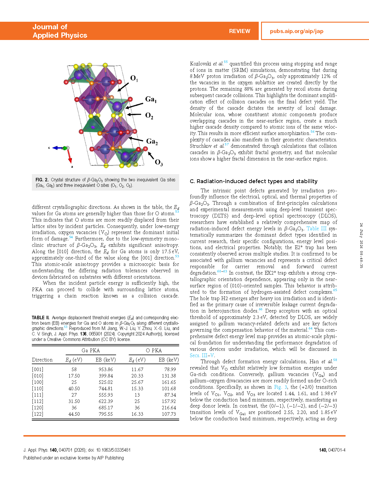
FIG. 2 Crystal structure of β-Ga₂O₃ showing the two inequivalent Ga sites (Ga₁, Ga₂) and three inequivalent O sites (O₁, O₂, O₃).
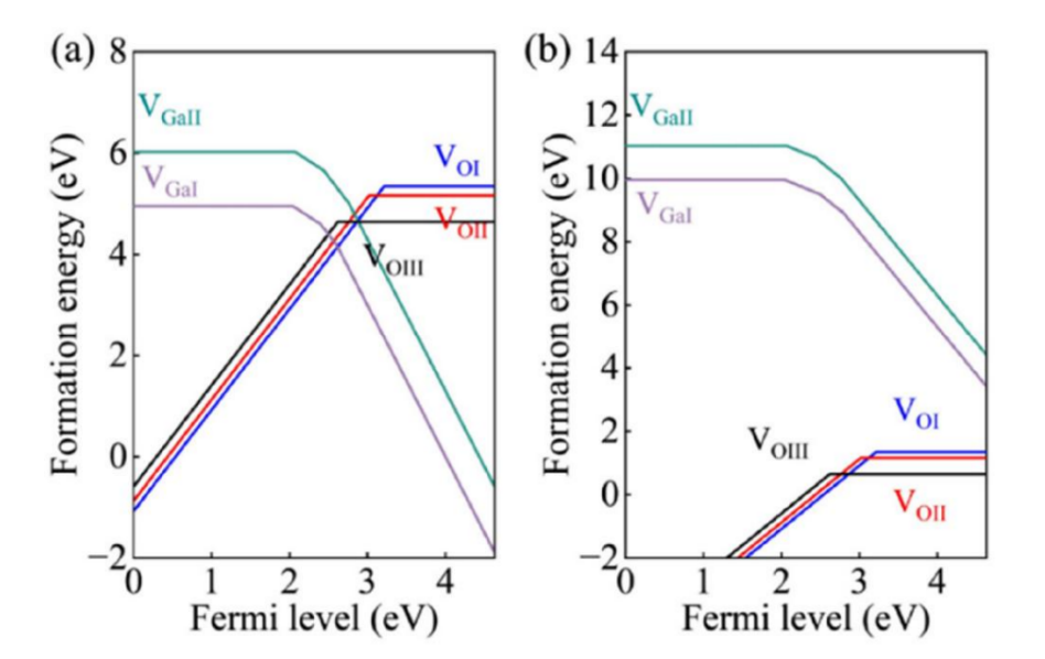
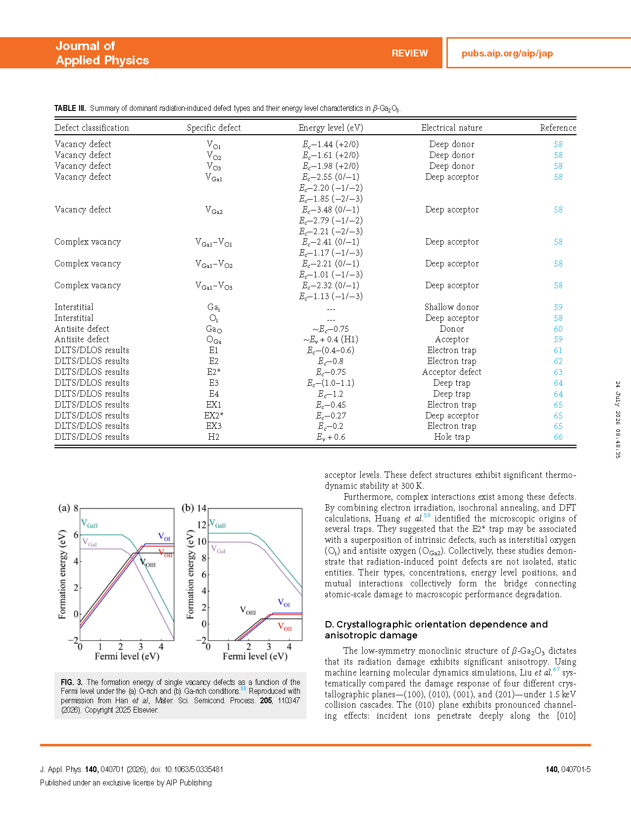
FIG. 3 The formation energy of single vacancy defects as a function of the Fermi level under the (a) O-rich and (b) Ga-rich conditions.
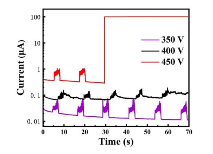
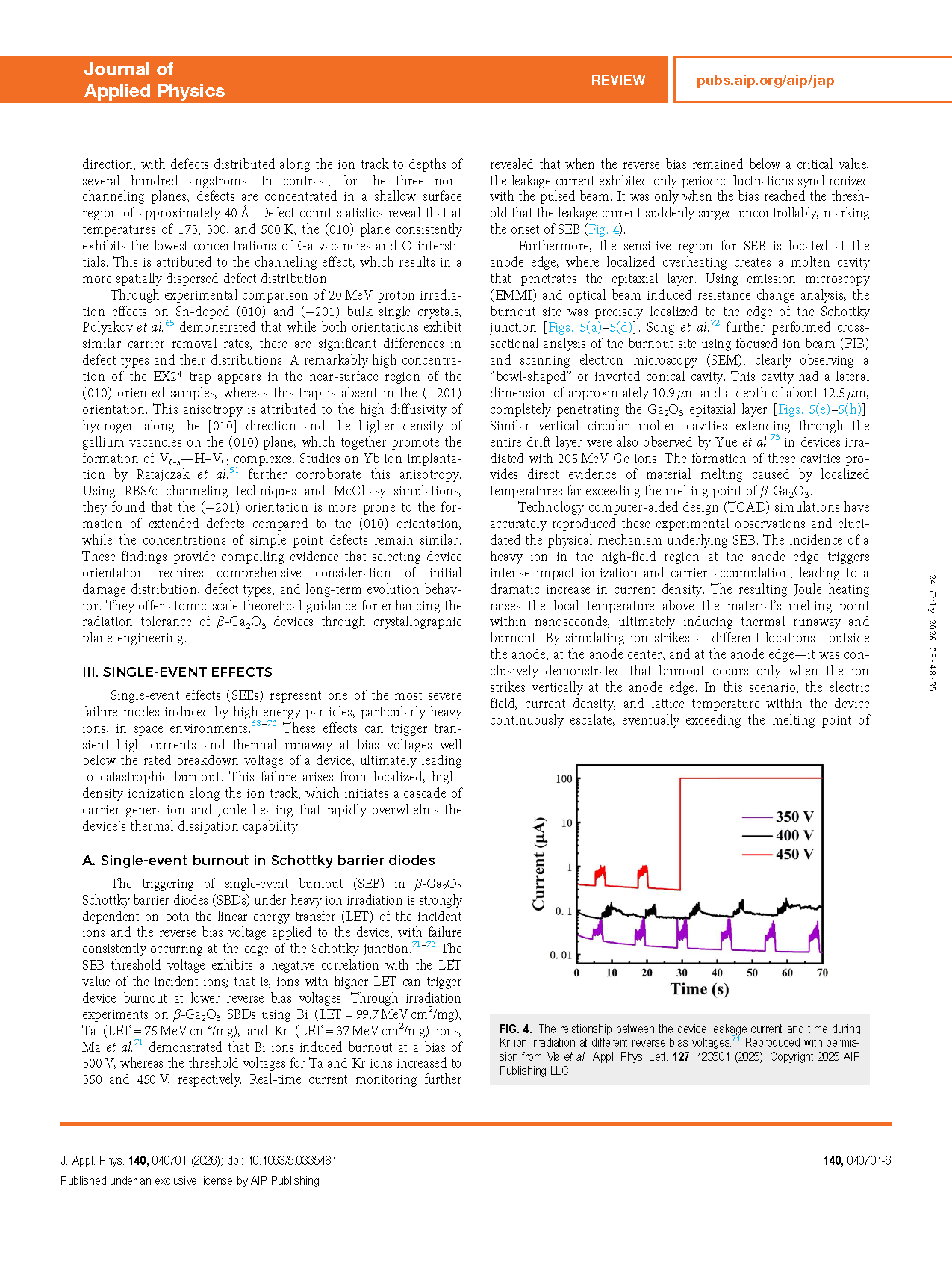
FIG. 4 The relationship between the device leakage current and time during Kr ion irradiation at different reverse bias voltages.
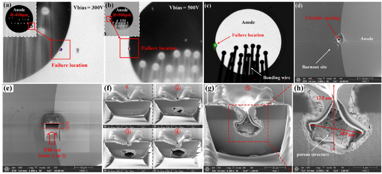
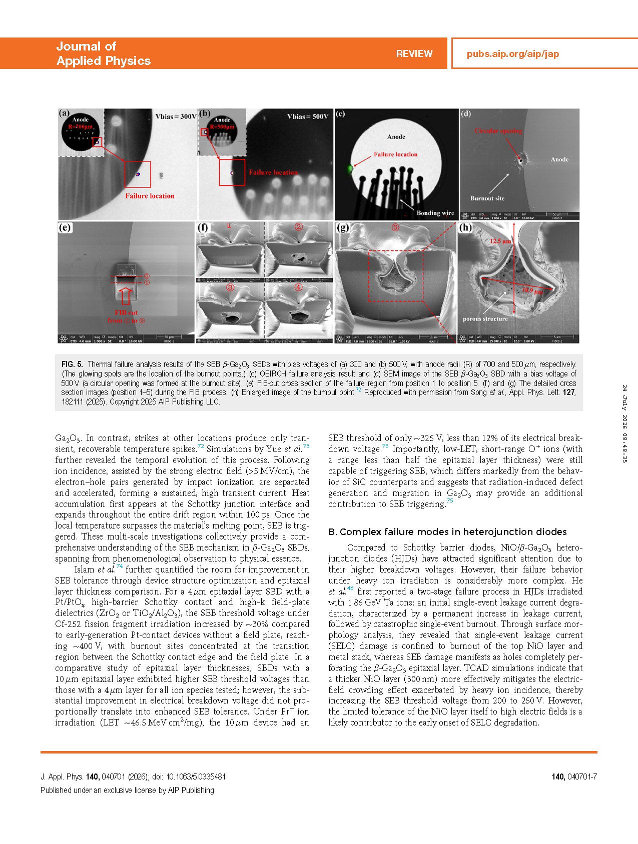
FIG. 5 Thermal failure analysis results of the SEB β-Ga₂O₃ SBDs with bias voltages of (a) 300 and (b) 500 V, with anode radii (R) of 700 and 500 μm, respectively. (c) OBIRCH failure analysis result and (d) SEM image of the SEB β-Ga₂O₃ SBD with a bias voltage of 500 V (a circular opening was formed at the burnout site). (e) FIB-cut cross section of the failure region from position 1 to position 5. (f) and (g) The detailed cross section images (position 1–5) during the FIB process. (h) Enlarged image of the burnout point.
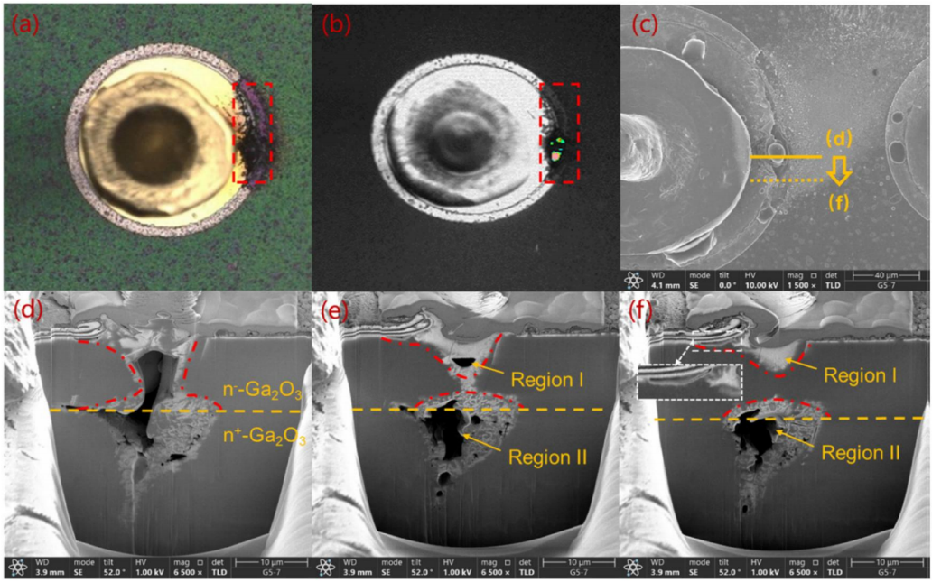
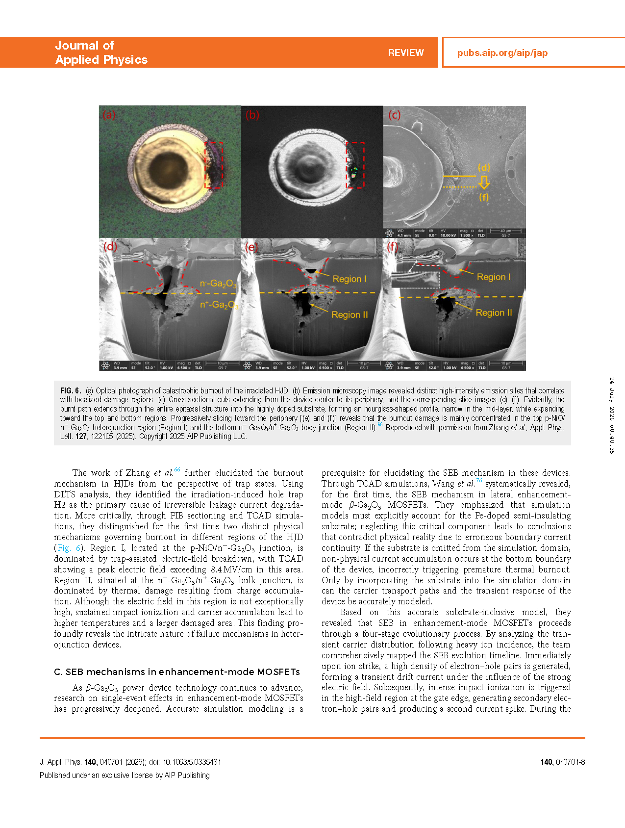
FIG. 6 (a) Optical photograph of the irradiated HJD. (b) Emission microscopy image revealed distinct high-intensity emission sites that correlate with localized damage regions. (c) Cross-sectional cuts extending from the device center to its periphery, and the corresponding slice images (d)–(f). Evidently, the burnt path extends through the entire epitaxial structure into the highly doped substrate, forming an hourglass-shaped profile, narrow in the mid-layer, while expanding toward the top and bottom regions. Progressively slicing toward the periphery [(e) and (f)] reveals that the burnout damage is mainly concentrated in the top p-NiO/n⁻-Ga₂O₃ heterojunction region (Region I) and the bottom n⁻-Ga₂O₃/n⁺-Ga₂O₃ body junction (Region II).
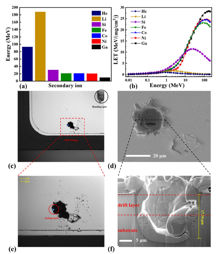
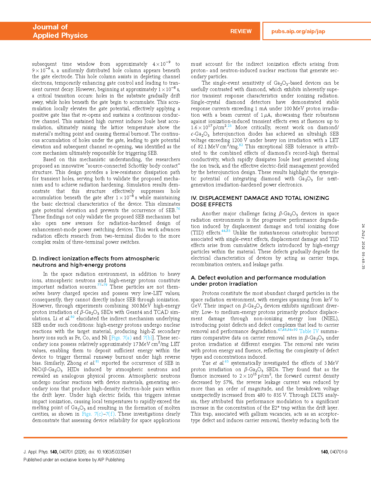
FIG. 7 (a) Energy and (b) LET distributions of secondary ions induced by 300 MeV proton for β-Ga₂O₃ SBD. (c) EMMI image of the NiO/β-Ga₂O₃ HJD. (d) SEM image of the burned spot on the device surface. (e) Abnormal luminescent spot on the device surface. (f) Cross-sectional image of the burned spot, with a maximum depth of 17.34 μm.
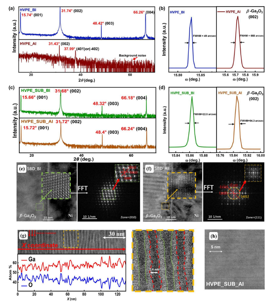
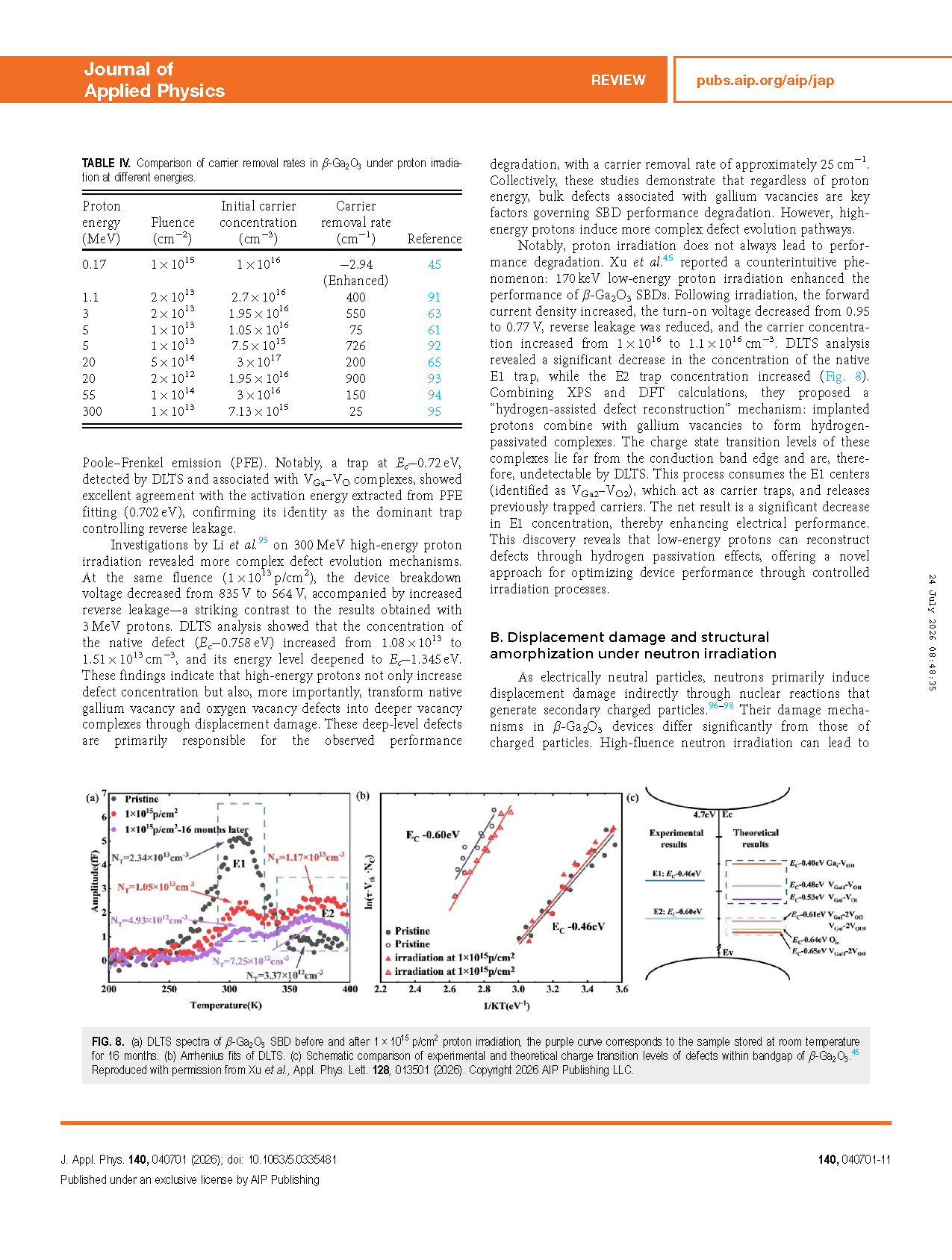
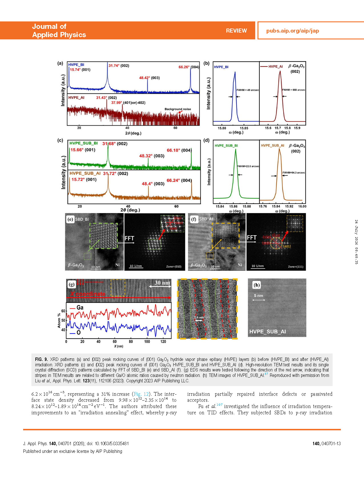
FIG. 8(a) XRD patterns (a) and (002) peak rocking curves of (001) Ga₂O₃ hydride vapor phase epitaxy (HVPE) layers (b) before (HVPE_BI) and after (HVPE_AI) irradiation. XRD patterns (c) and (002) peak rocking curves of (001) Ga₂O₃ HVPE_SUB_BI and HVPE_SUB_AI (d). High-resolution TEM test results and its single crystal diffraction (SCD) patterns calculated by FFT of SBD_BI (e) and SBD_AI (f). (g) EDS results were tested following the direction of the red arrow, indicating that stripes in TEM results are related to different Ga/O atomic ratios caused by neutron radiation. (h) TEM images of HVPE_SUB_AI.
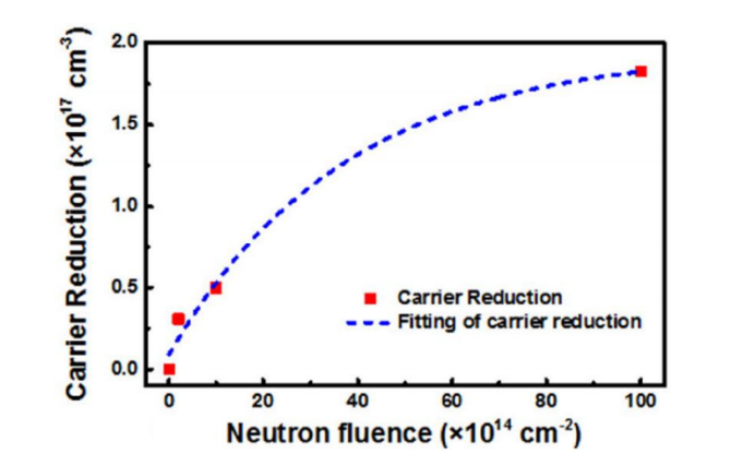
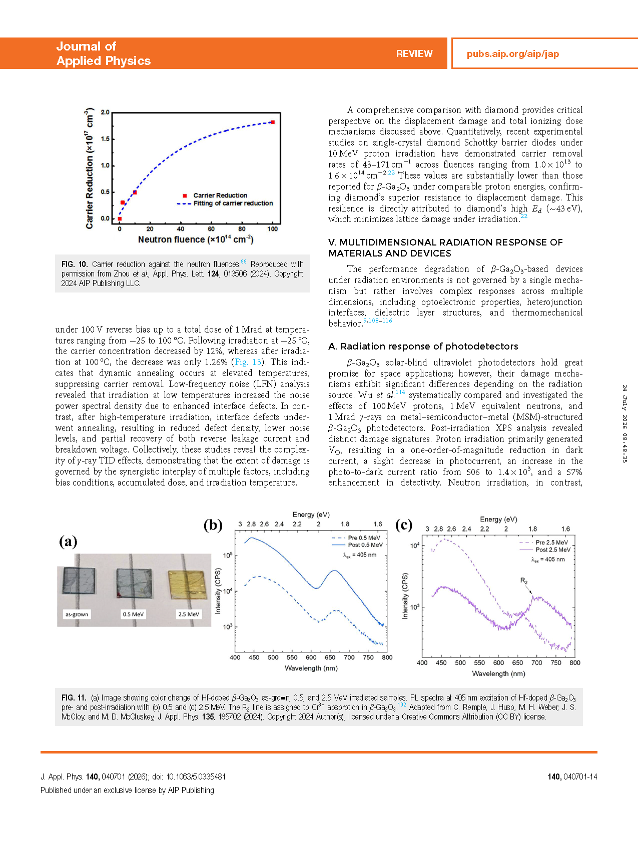
FIG. 9 Carrier reduction against the neutron fluences.
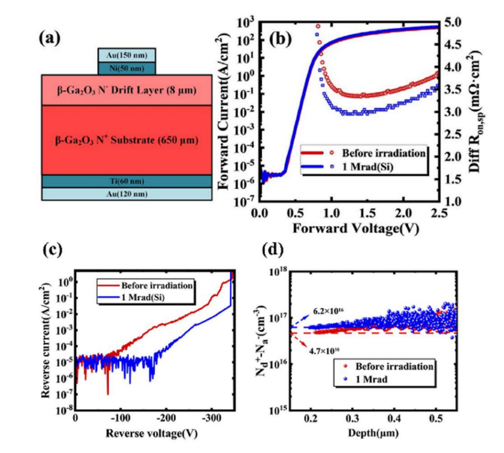
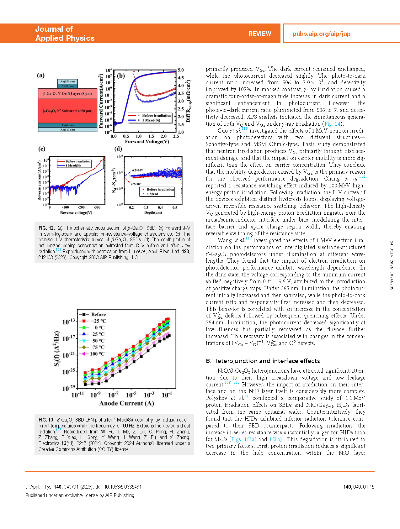
FIG. 10 (a) The schematic cross section of β-Ga₂O₃ SBD. (b) Forward J–V in semi-log-scale and specific on-resistance–voltage characteristics. (c) The reverse J–V characteristic curves of β-Ga₂O₃ SBDs. (d) The depth-profile of net ionized doping concentration extracted from C–V before and after γ-ray radiation.
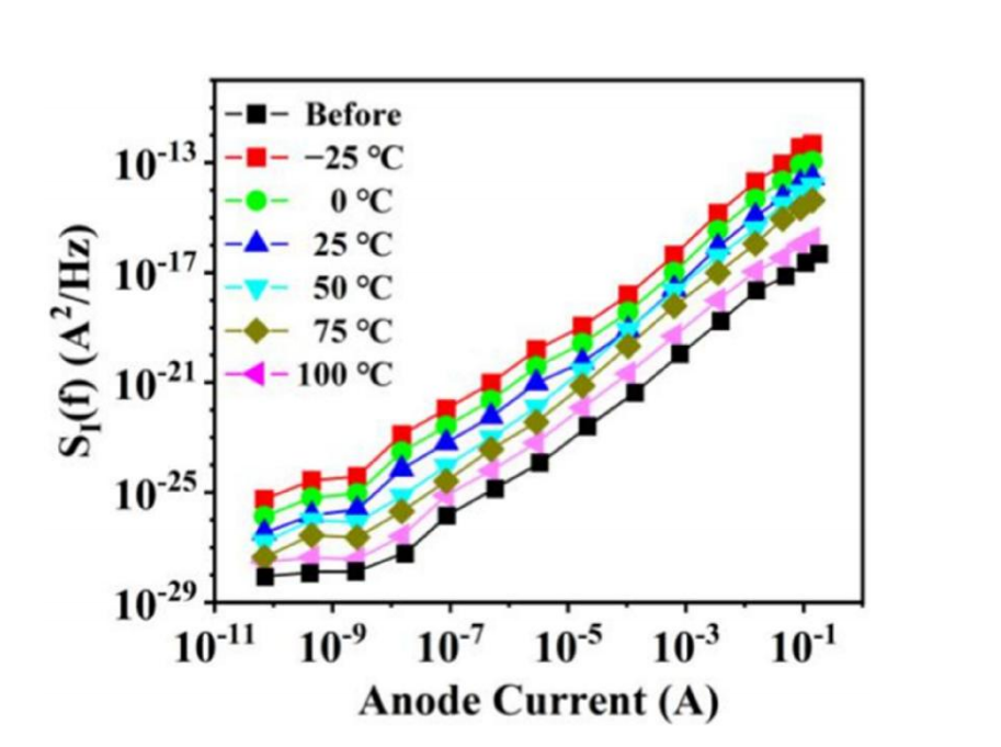
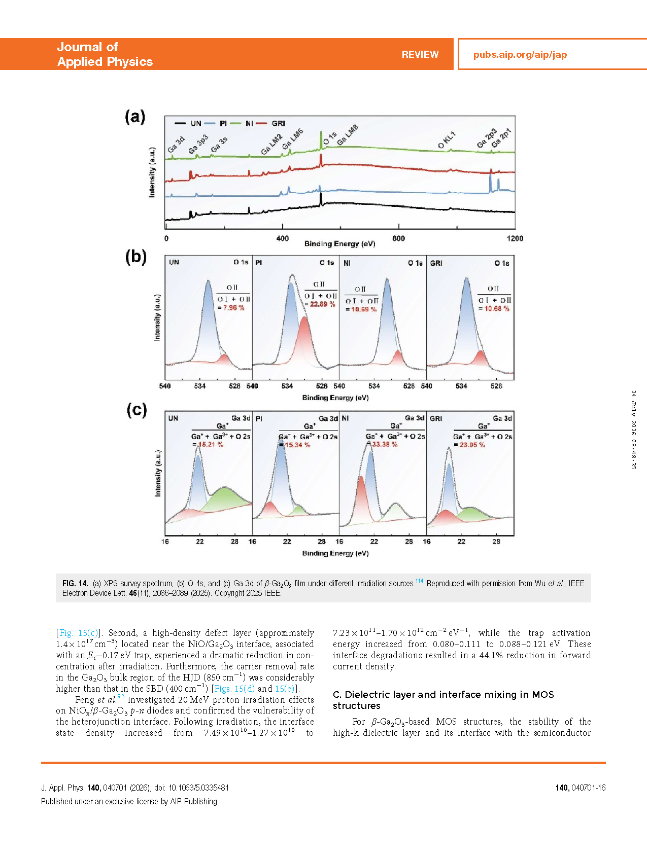
FIG. 11 β-Ga₂O₃ SBD LFN plot after 1 Mrad (Si) dose of γ-ray radiation at different temperatures while the frequency is 100 Hz. Before is the device without radiation.
DOI :
10.1063/5.0335481
Instruction
Official Account

Cooperation
Top
