


Background
Extreme ultraviolet (EUV) detectors are core components for extreme ultraviolet lithography, solar physics, high-resolution material characterization and other cutting-edge research fields. Silicon-based photodetectors dominate the current commercial EUV detection market with mature manufacturing processes and decent quantum efficiency. Nevertheless, silicon suffers severe radiation damage under high-flux high-energy EUV irradiation, generating numerous radiation-induced lattice defects, leading to continuous performance degradation and poor long-term operational reliability.
Ultra-wide bandgap semiconductors feature outstanding radiation tolerance, high thermal stability and robust chemical inertness, which can effectively suppress defect formation under high-energy particle bombardment. Among these materials, monoclinic gallium oxide (β-Ga₂O₃ ) exhibits superior visible-light transparency compared with diamond, AlGaN, silicon carbide and other wide-bandgap competitors, and mature controllable growth routes for β-Ga₂O₃ single crystals and thin films have been established.
Although β-Ga₂O₃ solar-blind ultraviolet photodetectors have been extensively investigated, its application potential in the 13.5 nm standard EUV band remains underexplored, and only a small number of published studies focus on gallium oxide EUV optoelectronic devices. Existing theoretical researches merely verify the preliminary feasibility of β-Ga₂O₃ EUV detectors, while a critical bottleneck restricts further device design: commercial TCAD simulation platforms lack complex refractive index and extinction coefficient datasets of β-Ga₂O₃ and p-type nickel oxide (NiO) in EUV wavelength range, disabling accurate device performance prediction. Besides, a unified multi-scale simulation framework covering atomic-scale material calculation and macroscopic heterojunction device simulation is absent to guide structural optimization of β-Ga₂O₃ EUV detectors.
As a low-cost, earth-abundant and chemically stable p-type wide-bandgap semiconductor, NiO can form p-NiO/i-β-Ga₂O₃ /n-β-Ga₂O₃ PIN heterojunctions with intrinsic β-Ga₂O₃ to realize efficient photogenerated carrier separation, yet the EUV optical parameters of NiO are also unreported. To solve the above limitations, this work adopts DFT+U first-principles calculations to supplement EUV optical constants of the two materials, constructs a complete multi-scale simulation platform, and carries out structural optimization, photoelectric response simulation and incident angle-dependent characteristic analysis of the heterojunction EUV photodetector.
Abstract
Highlights
The complex refractive indices (real and imaginary parts) of β-Ga₂O₃ and NiO at 13.5 nm EUV band are systematically calculated and supplemented via VASP DFT+U first-principles calculations, filling the vacancy of EUV optical parameters in commercial Sentaurus TCAD simulation software.
An integrated multi-scale simulation framework combining atomic-scale DFT material calculation and macroscopic TCAD device simulation is established for PIN-type β-Ga₂O₃/NiO heterojunction EUV photodetectors. The trap-assisted tunneling (TAT) model with E2 trap levels of β-Ga₂O₃ is imported to accurately reproduce the dark current characteristics of the heterojunction device.
The p-type doping concentration of NiO and thicknesses of NiO/i-β-Ga₂O₃ layers are comprehensively optimized, and the optimal device structure (25 nm NiO+100 nm intrinsic β-Ga₂O₃ ) is confirmed. The optimized detector realizes outstanding EUV detection performance with a photo-to-dark current ratio of 15760, external quantum efficiency of 433.5% and fast rise time of 1.8 μs.
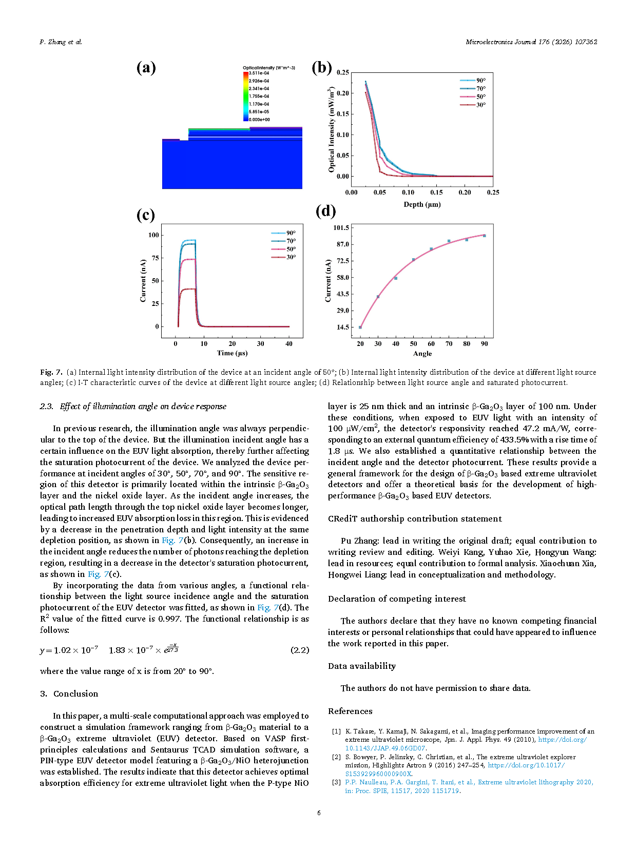
The influence of EUV incident angle (30°–90°) on saturated photocurrent is quantitatively analyzed, and a fitted mathematical function (y=1.02×10⁻⁷−1.83×10⁻⁷×e^(-x/27.3), 20°≤x≤90°) between incident angle and saturated photocurrent is derived, providing theoretical support for performance calibration under non-normal incidence conditions.
Conclusion
In this paper, a multi-scale computational approach was employed to construct a simulation framework ranging from β-Ga₂O₃ material to a β-Ga₂O₃ extreme ultraviolet (EUV) detector. Based on VASP first-principles calculations and Sentaurus TCAD simulation software, a PIN-type EUV detector model featuring a β-Ga₂O₃/NiO heterojunction was established. The results indicate that this detector achieves optimal absorption efficiency for extreme ultraviolet light when the P-type NiO layer is 25 nm thick and an intrinsic β-Ga₂O₃ layer of 100 nm. Under these conditions, when exposed to EUV light with an intensity of 100 μW/cm², the detector's responsivity reached 47.2 mA/W, corresponding to an external quantum efficiency of 433.5% with a rise time of 1.8 μs. We also established a quantitative relationship between the incident angle and the detector photocurrent. These results provide a general framework for the design of β-Ga₂O₃ based extreme ultraviolet detectors and offer a theoretical basis for the development of high-performance β-Ga₂O₃ based EUV detectors.
Project Support
This work is supported by the National Key Research and Development Program of China (2024YFE0213500), the Ji'an Natural Science Foundation Project (20255-071664), National Natural Science Foundation of China (12075045, 12335011), Fundamental and Interdisciplinary Disciplines Breakthrough Plan of the Ministry of Education of China (JYB2025XDXM107).
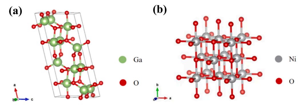
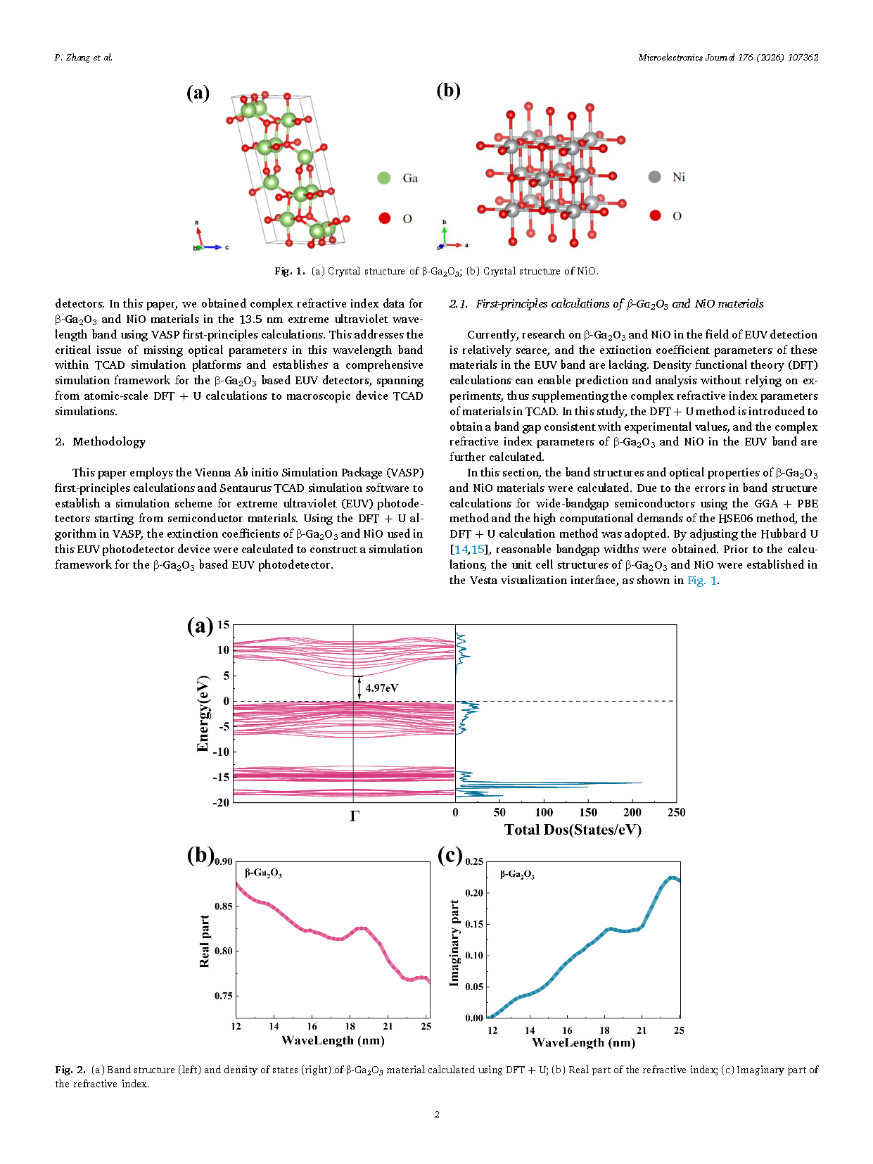
Fig. 1. (a) Crystal structure of β-Ga₂O₃ ; (b) Crystal structure of NiO.
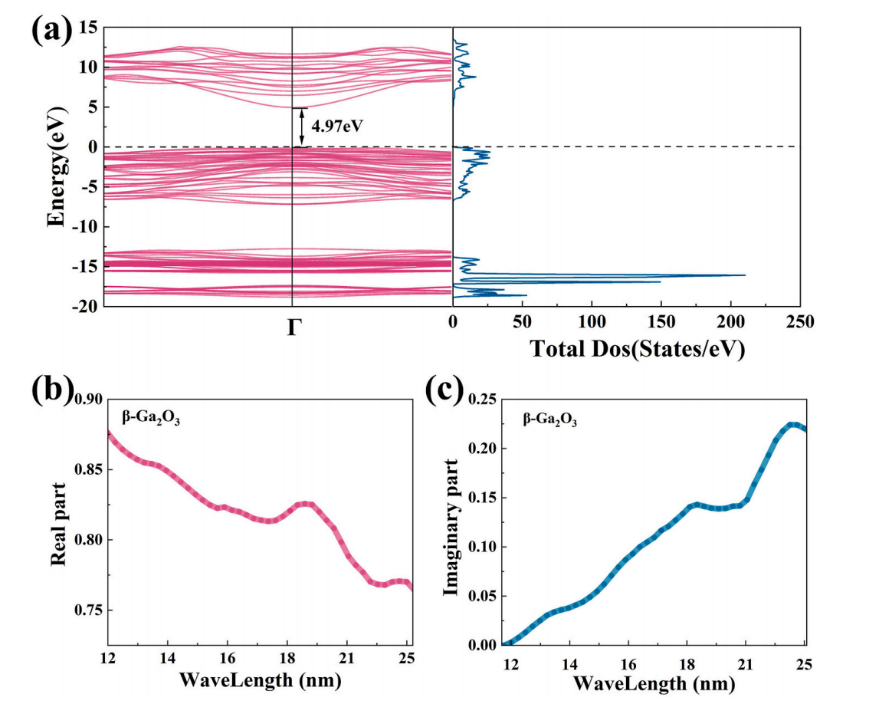
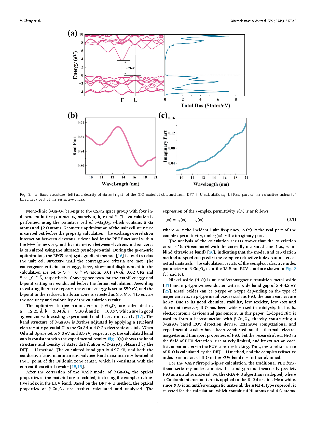
Fig. 2. (a) Band structure (left) and density of states (right) of β-Ga₂O₃ material calculated using DFT+U; (b) Real part of the refractive index; (c) Imaginary part of the refractive index.
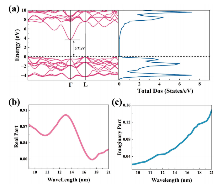
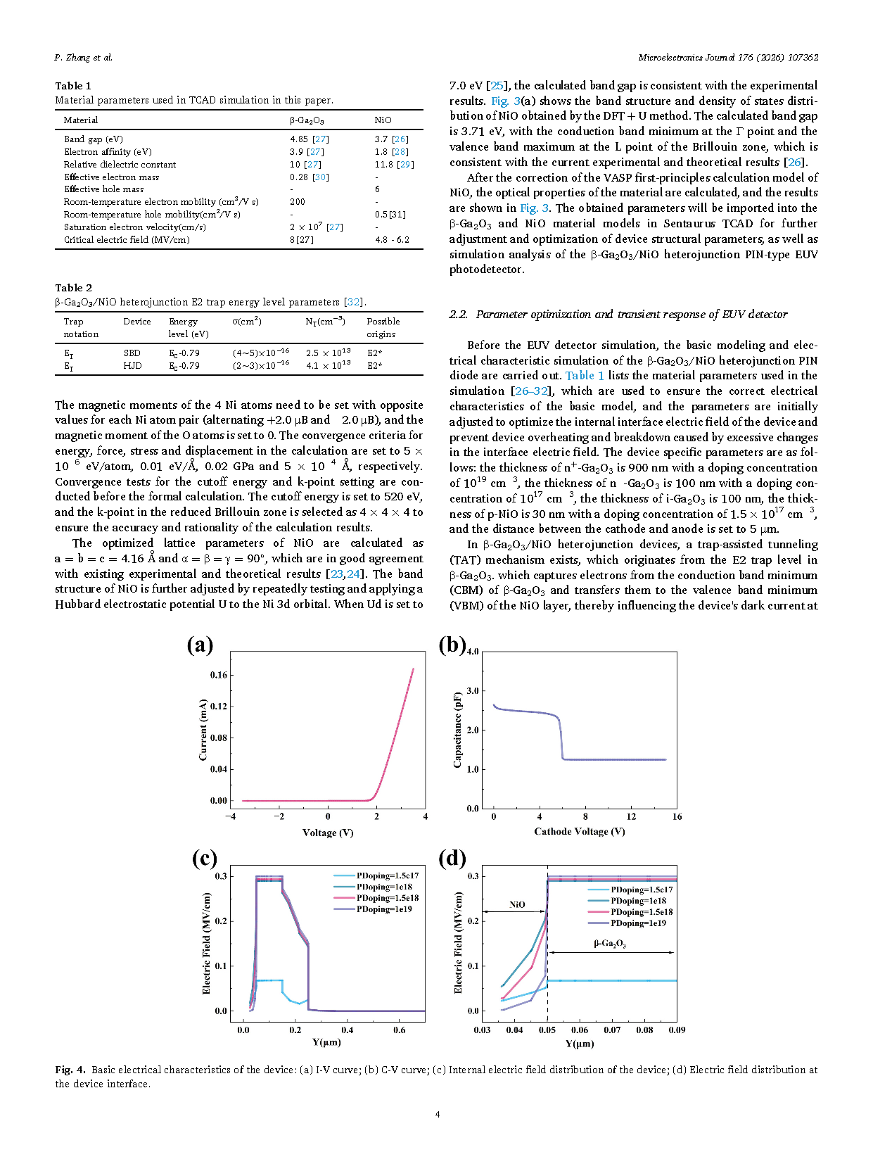
Fig. 3. (a) Band structure (left) and density of states (right) of the NiO material obtained from DFT+U calculations; (b) Real part of the refractive index; (c) Imaginary part of the refractive index.
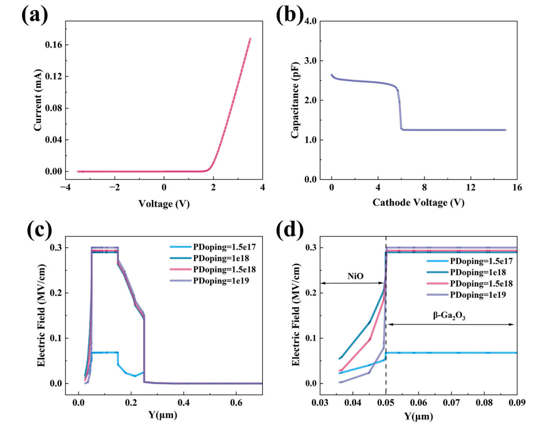
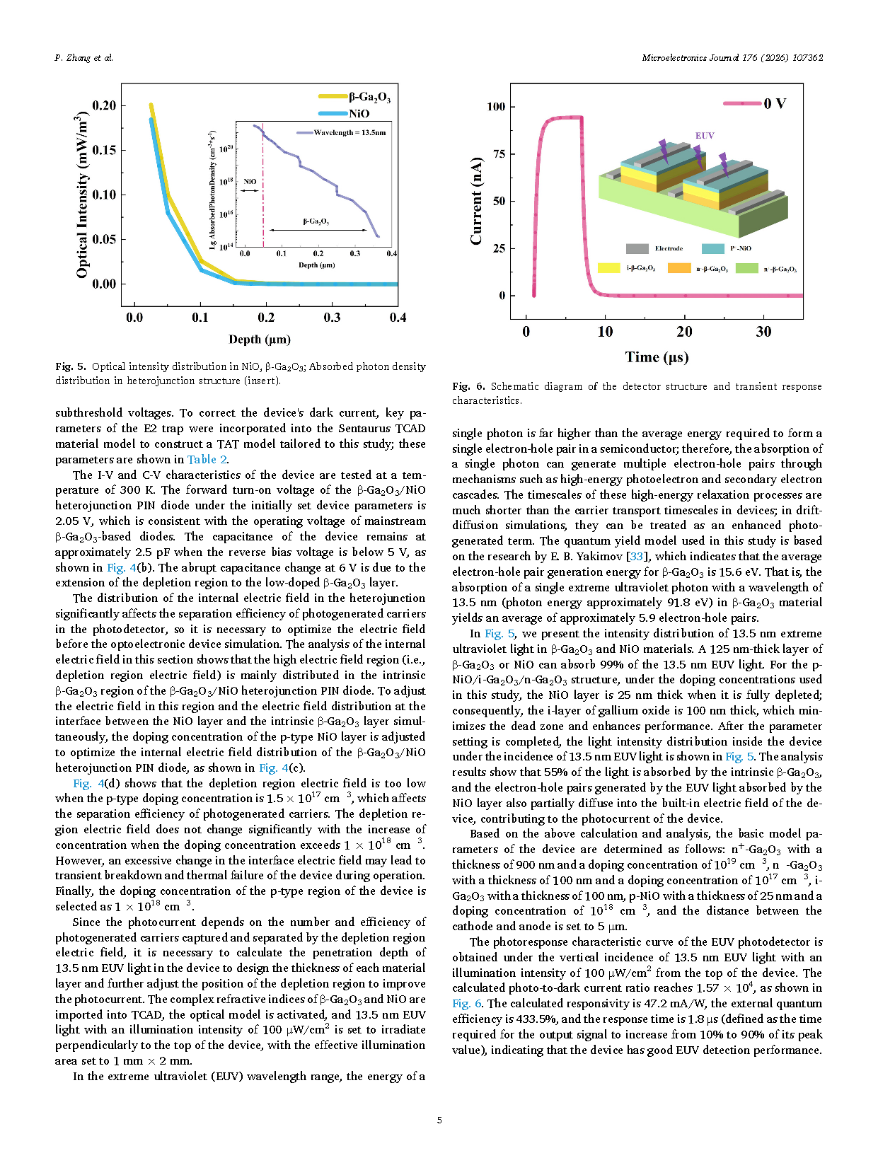
Fig. 4. Basic electrical characteristics of the device: (a) I-V curve; (b) C-V curve; (c) Internal electric field distribution of the device; (d) Electric field distribution at the device interface.
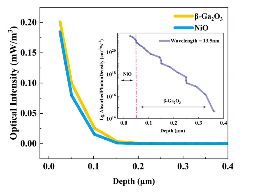
Fig. 5. Optical intensity distribution in NiO, β-Ga₂O₃ ; Absorbed photon density distribution in heterojunction structure (insert).
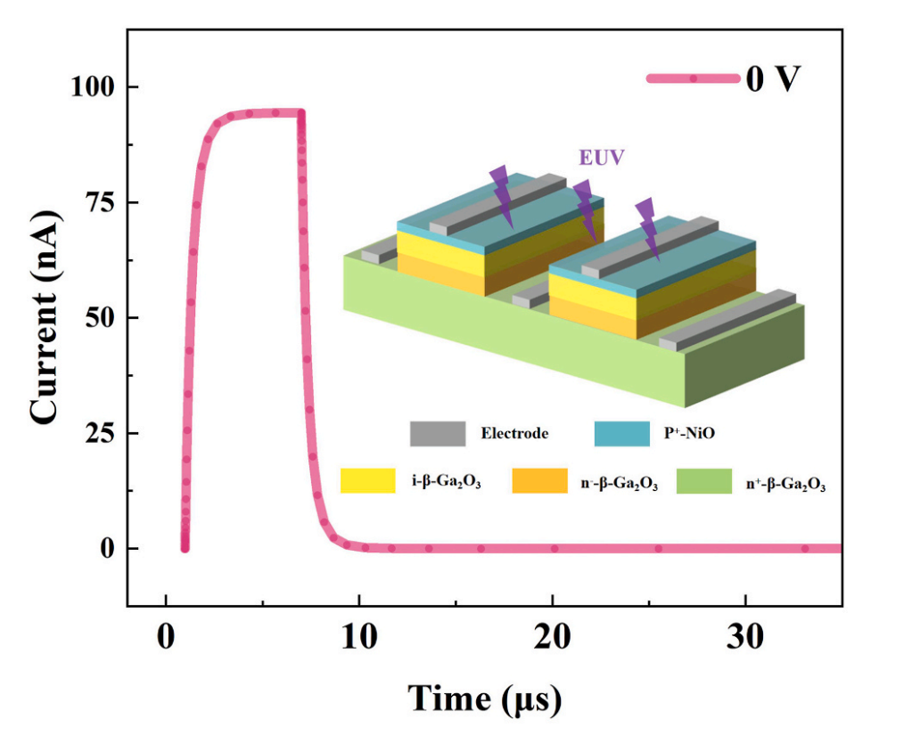
Fig. 6. Schematic diagram of the detector structure and transient response characteristics.
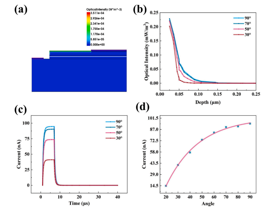
Fig. 7. (a) Internal light intensity distribution of the device at an incident angle of 50°; (b) Internal light intensity distribution of the device at different light source angles; (c) I-T characteristic curves of the device at different light source angles; (d) Relationship between light source angle and saturated photocurrent.
DOI :
10.1016/j.mejo.2026.107362
Instruction
Official Account

Cooperation
Top
