


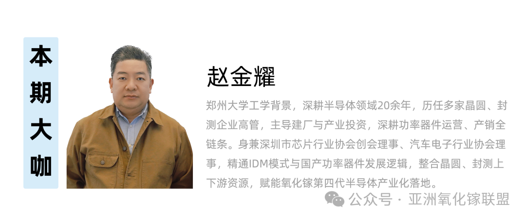
Beijing Orient Semi Co., Ltd. (“Orient Semi”) is headquartered in the Beijing Shunyi Science and Innovation Industrial Park, leveraging the local upstream resources for gallium oxide substrates and the downstream advantages of the new energy vehicle industry to develop its business. The company adopts an IDM vertically integrated manufacturing model, focusing on the R&D of gallium oxide epitaxial materials and high-voltage power device processes, wafer processing and manufacturing, foundry services, and sales. Its business model is partially benchmarked against Innoscience, a leading company in the gallium nitride industry. On the industrial side, the company works with leading domestic enterprises in alumina and gallium resources to establish a full-chain industrial ecosystem, while partnering with leading packaging and testing companies to improve supporting capabilities for downstream application implementation.
Editor’s Note
Silicon-based devices are approaching the limits of their physical performance, while silicon carbide (SiC) and gallium nitride (GaN) have ushered in the industrialization wave of third-generation semiconductors. Ultra-wide-bandgap (UWBG) materials represented by gallium oxide (Ga₂O₃) are now widely regarded as a key direction for next-generation power semiconductors.
Compared with previous generations of semiconductor materials, Ga₂O₃ offers one particularly notable advantage: superior high-voltage withstand capability, making it well suited to applications such as power transmission and specialized equipment. However, challenges in doping and heat dissipation remain major barriers to large-scale manufacturing.
In this issue of Chip Insights · Industry Leaders, we speak with Jinyao Zhao, Co-founder and General Manager of Beijing Orient Semi Co., Ltd., to explore the differentiated value of the Ga₂O₃ sector, key technological challenges, commercialization pathways, and its long-term development prospects.
Breaking Out of Silicon’s Crowded Market to Capture the Blue Ocean of Ga₂O₃
Huanshi: Mr. Zhao, you began your career in semiconductor sales, working with imported chips and domestic component distribution, and in recent years you have shifted your focus to gallium oxide by co-founding Beijing Orient Semi Co., Ltd. What industry outlook drove this transition?
Jinyao Zhao: I have worked in the semiconductor industry for more than 20 years, and I have always remained deeply involved in the sector. My decision to make a firm transition into fourth-generation semiconductors stems primarily from my long-term observation of how the industry evolves.
Today, silicon-based chips account for more than 91% of the global market. The technology is mature and the supply chain is well established, but silicon has already approached its physical performance limits. Meanwhile, key patents, manufacturing processes, and core equipment remain dominated by overseas players. As a result, Chinese companies can largely only follow the existing players in this mature market, making it difficult to achieve a breakthrough and overtake incumbents.
By contrast, domestic companies have already achieved breakthroughs in some areas of third-generation semiconductors such as silicon carbide (SiC) and gallium nitride (GaN). Innoscience, for example, was not the earliest entrant into GaN, but it has grown into a global leading company through a mature industrialization strategy.
This also demonstrates that emerging semiconductor sectors are not yet locked into established monopolies, giving Chinese companies an opportunity to change tracks and take the lead. We therefore believe that fourth-generation semiconductors, represented by gallium oxide (Ga₂O₃), offer a critical direction for deepening our involvement in the semiconductor industry and creating long-term value.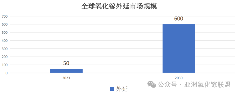
(Data sources: Yole Développement and Wolfspeed financial reports)
Huanshi: You see an opportunity for fourth-generation semiconductors to overtake incumbents by changing tracks. Could you break down the key differentiated advantages of gallium oxide (Ga₂O₃) compared with silicon, silicon carbide, and gallium nitride, and explain where its unique market opportunities lie?
Jinyao Zhao: The core driver of semiconductor material evolution is breaking through the performance limitations of previous-generation materials. Silicon-based devices offer high maturity and controllable costs, making them well suited to conventional applications such as consumer electronics and general-purpose home appliances. However, their voltage withstand capability and conduction performance are limited, making them less suitable for extremely demanding operating conditions.
After more than a decade of development, silicon carbide (SiC) and gallium nitride (GaN) have entered a relatively mature stage of industrialization, with their performance boundaries becoming increasingly well established.
Gallium oxide (Ga₂O₃), by contrast, offers key advantages including an ultra-wide bandgap, extremely high voltage withstand capability, and low conduction losses. These characteristics give it potential in areas where conventional semiconductor materials face performance constraints. In demanding applications such as ultra-high-voltage power transmission, energy-efficient computing centers, specialized radar systems, and high-precision navigation, Ga₂O₃ devices could enable lower power consumption and greater operational stability, opening up new opportunities in the high-end power semiconductor market.
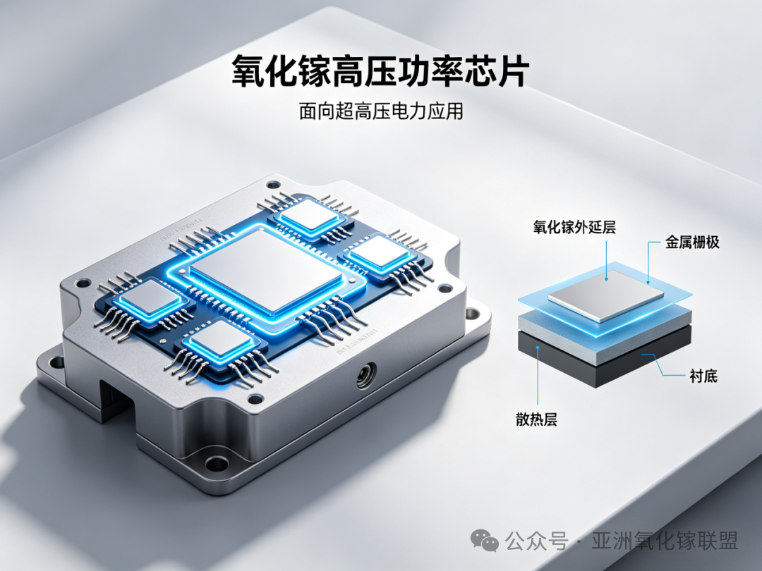
One of the application scenarios for gallium oxide
Huanshi: So, rather than simply replacing existing devices, Ga₂O₃ is opening up a new set of application scenarios that conventional devices have not been able to adequately support.
Jinyao Zhao: We believe that every type of semiconductor device has its own optimal application range. Silicon devices, for example, are highly mature and therefore well suited to consumer electronics and general-purpose home appliances. However, when it comes to ultra-high-voltage applications and complex operating conditions, new materials are needed to fill the capability gap.
Fourth-generation semiconductor materials include diamond, aluminum nitride (AlN), and gallium oxide (Ga₂O₃), each with its own advantages. Diamond offers outstanding performance, but its material synthesis and device fabrication are extremely challenging, making large-scale commercialization difficult in the short term. After a comprehensive comparison, our team is more optimistic about the development prospects of Ga₂O₃.
Huanshi: I’d like to ask further about the current maturity of the overall Ga₂O₃ technology roadmap. Have any Ga₂O₃ devices already entered the commercial stage?
Jinyao Zhao: Based on publicly available industry information, we believe the technology roadmap is still in the experimental and accelerated validation stage, and it is not yet ready for large-scale commercialization in the short term. There are two major bottlenecks: doping and device thermal management. These two factors directly determine the ultimate application capabilities of the devices.
Regardless of the type of power device, the technology ultimately has to be validated in real-world applications. Without addressing these two major challenges, it will be difficult to achieve large-scale deployment. As mentioned earlier, target applications such as power transmission and specialized navigation impose stringent requirements on device power consumption, thermal management, and reliability.
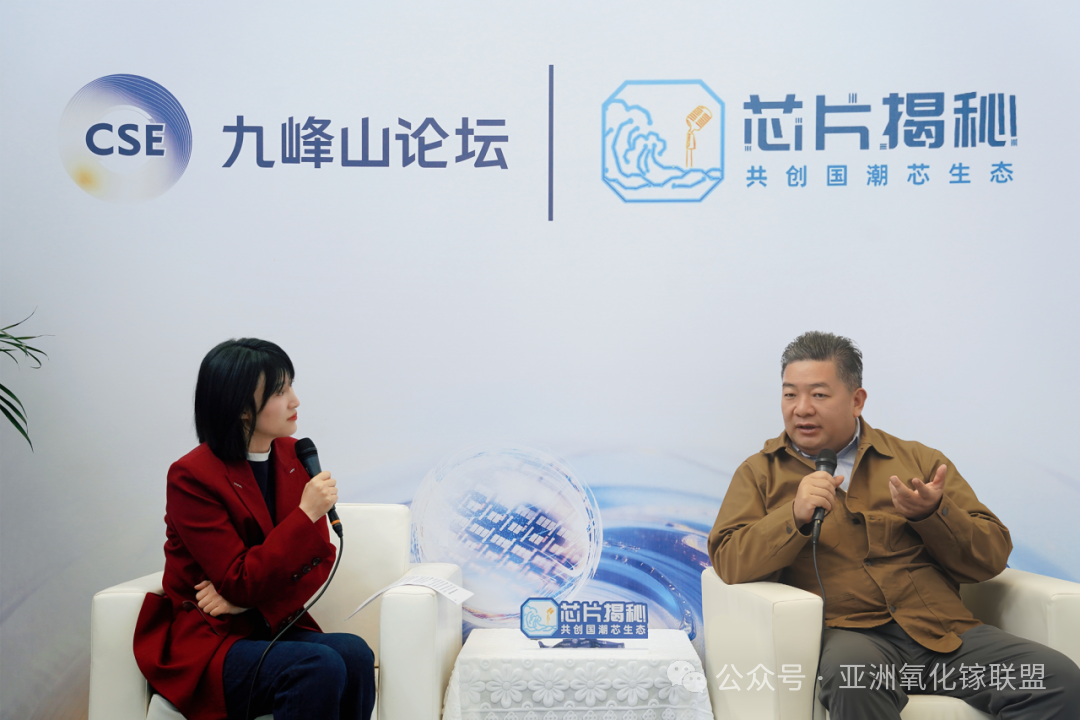
Chip Insights Founder Cao Huanshi (left) in conversation with Jinyao Zhao (right),
Co-founder and General Manager of Beijing Orient Semi Co., Ltd.
Racing Alongside Global Players: The Window of Opportunity for Ga₂O₃ Industrialization
Huanshi: Given the current state of the industry, what has Beijing Orient Semi Co., Ltd. laid out in the Ga₂O₃ sector? What stage have you reached, and do you already have sample wafers or products?
Jinyao Zhao: Our founding team, together with our upstream substrate-material shareholder, has accumulated a solid foundation across various segments of the Ga₂O₃ materials and device value chain. At present, we are focusing on the industrialization of Ga₂O₃ epitaxial processes, working with Jiufengshan Laboratory and several universities on research collaborations and pilot-scale development, with priority given to establishing large-scale epitaxial production capabilities.
On this basis, we are using our own investment and supporting equipment to fabricate devices and advance engineering validation and wafer processing services. Only after we have achieved breakthroughs in a series of critical technologies and service capabilities will we work with more application-side industry partners to drive Ga₂O₃ toward broader commercial deployment.
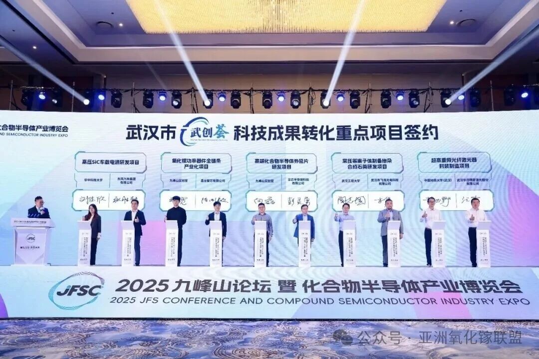
Signing Ceremony for the Cooperation between Jiufengshan Laboratory and Beijing Orient Semi Co., Ltd.
(Image source: Beijing Orient Semi Co., Ltd.)
Huanshi: You just mentioned epitaxial technology. It seems that there is still a supply gap for Ga₂O₃ epitaxial products in China, and the level of domestic substitution remains relatively low. How are overseas players progressing?
Jinyao Zhao: At present, China has yet to establish a fully stable and mature supply system for Ga₂O₃ epitaxial materials. NCT, a representative overseas company, announced last year that it had produced engineering-batch samples, but there has not yet been any clear evidence of large-scale commercial deliveries in the market.
We believe there are two possible explanations. On the one hand, frontier technologies may be subject to technological barriers or restrictions. On the other hand, the relevant technology route may not yet have achieved the expected results and therefore requires further iteration and development.
Ga₂O₃ Epitaxy
(Image source: Beijing Orient Semi Co., Ltd.)
Huanshi: Based on this, would you say that the first applications of Ga₂O₃ are likely to emerge in specialized industries?
Jinyao Zhao: In fact, the semiconductor industry as a whole has often followed a “military first, civilian later” development path. At the early stage of an emerging technology, specialized markets with strong demand can accommodate new technologies. Cost is less of a short-term concern, allowing products to undergo continuous validation, testing, and iteration. Once the technology matures, it can gradually expand from specialized applications into civilian markets.
Although Ga₂O₃ is known as a fourth-generation semiconductor material, it still has market continuity and industrial connections with the previous three generations. Its technological evolution is a gradual process, and it is difficult for an entirely new material to enter the market independently without connecting to existing application ecosystems.
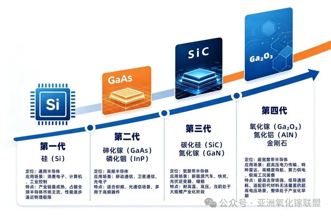
Evolution of Four Generations of Semiconductor Materials
Huanshi: Strong technological barriers overseas may be partly due to the fact that these technologies were initially concentrated in specialized applications. They are unlikely to make it easy for us to catch up. In a sense, you are among the pioneers venturing into this emerging field.
Jinyao Zhao: Exactly. We are pioneers.
Huanshi: From what I’ve heard, this sector requires the integration of substantial resources and the development of a long industrial chain—from substrates and epitaxy to devices and supporting equipment. What gives your team the confidence to keep investing in this field?
Jinyao Zhao: We can look to the track-changing success of Innoscience in the GaN sector as a reference. Innoscience was not the earliest entrant into the industry, but ultimately grew into a global leading company, providing a clear example for those who followed.
From another perspective, the development of third-generation semiconductors also offers valuable lessons. Emerging wide-bandgap semiconductor sectors may likewise have the potential to follow a similar growth trajectory. The material properties of Ga₂O₃ have already been theoretically validated and have received preliminary experimental verification in specialized and high-voltage power applications, giving the material considerable long-term development potential.
From Samples to Commercialization: Outlook for the Ga₂O₃ Development Cycle
Huanshi: Have any other companies in the industry managed to release Ga₂O₃ device samples?
Jinyao Zhao: At present, most participants in this field are still research institutions. Commercial companies are largely focused on upstream materials such as substrates and epitaxial precursors, while there are still relatively few achievements on the device side. Through collaboration with research institutions, Beijing Orient Semi Co., Ltd. has completed the development of Ga₂O₃ device samples, placing us relatively early in the industry.
Huanshi: Could you briefly introduce the form of your device samples and their target application scenarios?
Jinyao Zhao: Building on our epitaxial processes, we have developed Ga₂O₃ Schottky barrier diodes (SBDs) and Ga₂O₃ MOS power devices, which can be used for preliminary engineering testing and validation by laboratories, research institutions, and selected engineering customers.
In late April, we also began discussions with several leading companies in the power equipment sector. These companies specialize in high-voltage power transmission and distribution equipment, and ultra-high-voltage power applications are among the key high-value-added scenarios we are prioritizing for the commercialization of Ga₂O₃.
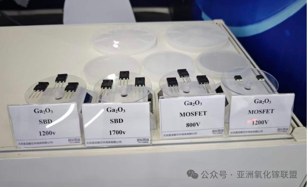
Ga₂O₃ SBD and MOS Devices
(Image source: Beijing Orient Semi Co., Ltd.)
Huanshi: It is widely recognized in the industry that Ga₂O₃ has relatively low thermal conductivity, significantly lower than that of SiC. Could thermal management constraints limit its deployment in power applications?
Jinyao Zhao: Thermal management is indeed a core challenge that cannot be avoided. Like doping, it is an inherent challenge arising from the material's intrinsic properties. We are currently working with partners across the materials sector, research institutions, and Changjiang Optoelectronics Industry Investment to make early investments in thermal management and advanced packaging. We are exploring viable approaches to improving thermal management through adjustments to material preparation processes, epitaxial film designs, and customized packaging solutions.
Huanshi: So substantial process optimization will still be needed going forward. Let me ask next: How does Beijing Orient Semi position its business model? Would you describe it as an IDM or a fabless IDM model?
Jinyao Zhao: At this stage, we position ourselves as a lightweight IDM model.
Huanshi: A fully integrated, asset-heavy approach requires significant investment. Have you considered focusing on a single segment—for example, materials or device design—and pursuing a more asset-light development strategy?
Jinyao Zhao: From the perspective of long-term industrial development, if a company wants to master core technologies and gain a strong voice in the industry, the IDM model is more conducive to building leadership across the value chain. If we focus on only one segment, it would be difficult to establish a truly irreplaceable core competitive advantage.
Huanshi: An end-to-end strategy also means substantial capital expenditure and technical challenges across multiple stages. How do you plan to address the funding requirements?
Jinyao Zhao: During the Jiufengshan exhibition in April, we held in-depth discussions and reached cooperation intentions with upstream domestic material suppliers, Changjiang Optoelectronics Industry Investment, and other industry players and investment institutions. As the industry continues to gain traction and the technology advances, industrial capital will develop a deeper understanding of this emerging sector. As long as we can bridge the gap between technology and the market, the funding pressure may become much easier to address.
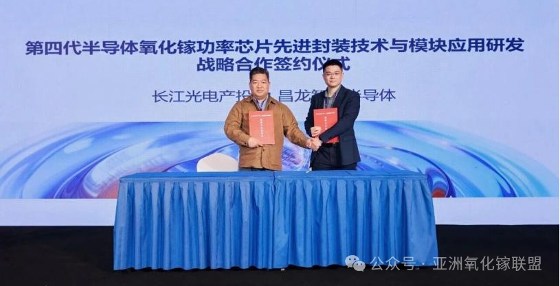
Signing Ceremony for the Cooperation between Changjiang Optoelectronics Industry Investment and Beijing Orient Semi Co., Ltd.
(Image source: Beijing Orient Semi Co., Ltd.)
Huanshi: As a pioneer in this emerging field, how do you assess the overall maturation timeline for Ga₂O₃ devices? What challenges still need to be overcome before the industry can achieve full-scale commercialization?
Jinyao Zhao: We estimate that another one to two years of foundational technical development will be needed for epitaxial material processes and device manufacturing lines, while large-scale industry growth will likely require another three to five years.
The key challenges ahead remain technological breakthroughs, particularly in epitaxial growth processes, controllable doping solutions, and the thermal management issues we discussed earlier. Once substantial progress is made in these areas, Ga₂O₃ is expected to reach a broader commercialization window in applications such as power transmission, power supplies for computing infrastructure, and specialized equipment.
Industry–Academia–Research Collaboration: Building Momentum for Long-Term Growth
Huanshi: What form does the collaboration between Beijing Orient Semi Co., Ltd. and Jiufengshan Laboratory take? Does the technical cooperation cover substrates, epitaxy, or device development?
Jinyao Zhao: Jiufengshan Laboratory focuses primarily on compound semiconductors, with gallium oxide (Ga₂O₃) being an important area within its research portfolio. The two sides bring complementary strengths: we have our own technology roadmap and an industrial team, while the laboratory has well-established equipment platforms and strong R&D capabilities.
Our collaboration with Jiufengshan Laboratory is not primarily focused on substrate materials. Instead, it centers on epitaxial validation and device development, which closely aligns with our own R&D priorities.
Huanshi: Are the two sides planning to jointly establish a new company to advance the project?
Jinyao Zhao: There are no such plans for the time being. The collaboration will mainly focus on joint technology development and iteration. The laboratory will contribute equipment and R&D personnel, while the ownership of technological achievements will be handled through joint ownership or differentiated ownership arrangements, depending on the specific project.
Huanshi: Essentially, this is a co-built experimental transformation platform that lowers the early R&D costs for startups through intensive investment, which is also a clever move in the industrial layout of Wuhan Optics Valley. Having spent more than 20 years deeply rooted in the semiconductor industry, what advice do you have for young professionals who aspire to enter the semiconductor sector, especially the wide-bandgap field?
Jinyao Zhao: In the early days, the industry threshold was relatively limited. With intensifying technological competition, the threshold continues to rise, and the industry has gradually shifted from following overseas players to independent innovation. Against the backdrop of external technological blockades, China's semiconductor industry has great potential. I suggest that young people who have the opportunity to enter this industry can settle down and cultivate it for the long term, treating semiconductors as a long-term career. The room for development is well worth looking forward to.
Huanshi: Therefore, semiconductors remain an industry worthy of long term dedication. It will not be replaced by AI, and abundant opportunities lie ahead.
Jinyao Zhao: Many young people around me have chosen semiconductor related majors upon my advice. My nephew is one such example. He was admitted to Xidian University on my recommendation and enrolled in a PhD program in optoelectronics at Huazhong University of Science and Technology last year. My advice to him at that time was that China’s optoelectronics sector was still in its infancy. Steady, step by step progress along this path will unlock enormous potential.
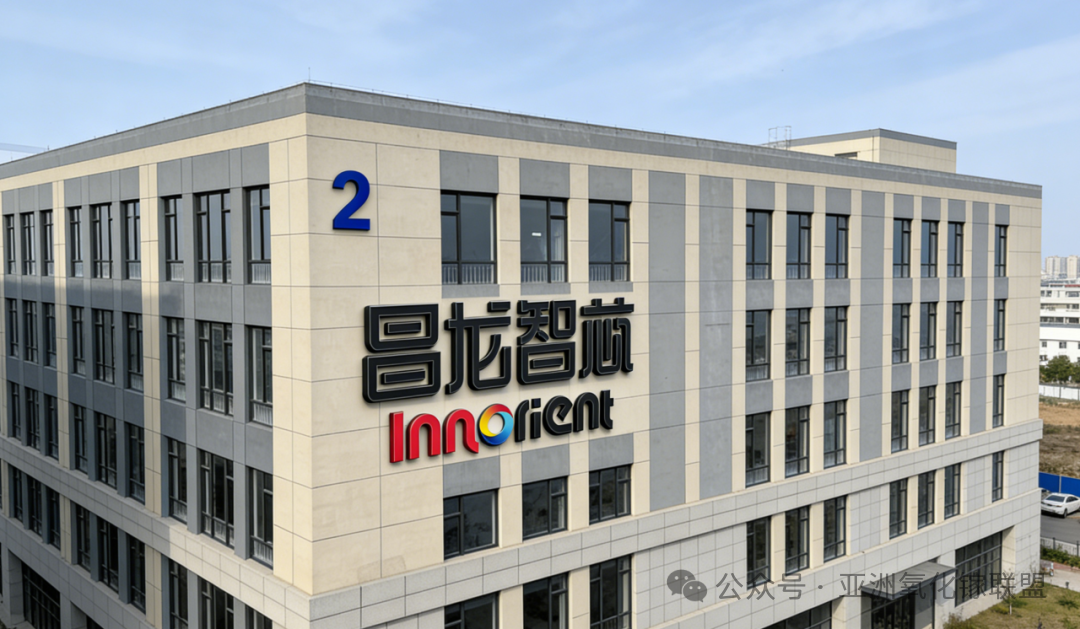
Beijing Orient Semi Production Facility
(Image source: Beijing Orient Semi Co., Ltd.)
Huanshi: You are also personally encouraging and guiding younger people to enter the semiconductor industry, which shows just how confident you are in this field. As an emerging sector, Ga₂O₃ offers Chinese companies a relatively level playing field with overseas players, creating opportunities to keep pace with global leaders and even take the lead in certain areas. We look forward to seeing more technological progress from Beijing Orient Semi and would be delighted to have you back on Chip Insights to share your latest developments.
Jinyao Zhao: Absolutely. Thank you.
Instruction
Official Account

Cooperation
Top
