


Researchers from Tianjin University of Technology, Peking University Shenzhen Graduate School, Guangdong Provincial Key Laboratory of Nano-Micro Materials Research have published a research article titled "Interface-Engineered Ga₂O₃/(AlₓGa₁₋ₓ)₂O₃/GaN Heterojunction Photodetectors with Tunable Band Alignment and Enhanced Carrier Separation" in Journal of Alloys and Compounds.
Background
Dual-band photodetectors responding to solar-blind and UV-A light play vital roles in flame monitoring, environmental monitoring, secure UV communication and space exploration. Monoclinic Ga₂O₃ with an intrinsic 4.9 eV bandgap realizes solar-blind detection, while GaN absorbs UV-A light at 365 nm, and their heterostructures enable single-chip broadband UV detection. Conventional direct Ga₂O₃/GaN heterojunctions own small conduction band offset, which cannot block electron injection from GaN under reverse bias, resulting in high dark current, severe carrier recombination and limited responsivity and detectivity. Existing researches only adopt fixed-composition (AlₓGa₁₋ₓ)₂O₃ interlayer without systematic study on the coupling effect of Al content on surface morphology, defect density and band alignment. There is no quantitative analysis of the competition among Al composition, interfacial defects and carrier transport, and no multifunctional photodetector design supporting UV encrypted logic communication. This forms a critical research gap restricting the industrialization of broadband UV heterojunction photodetectors.
Abstract
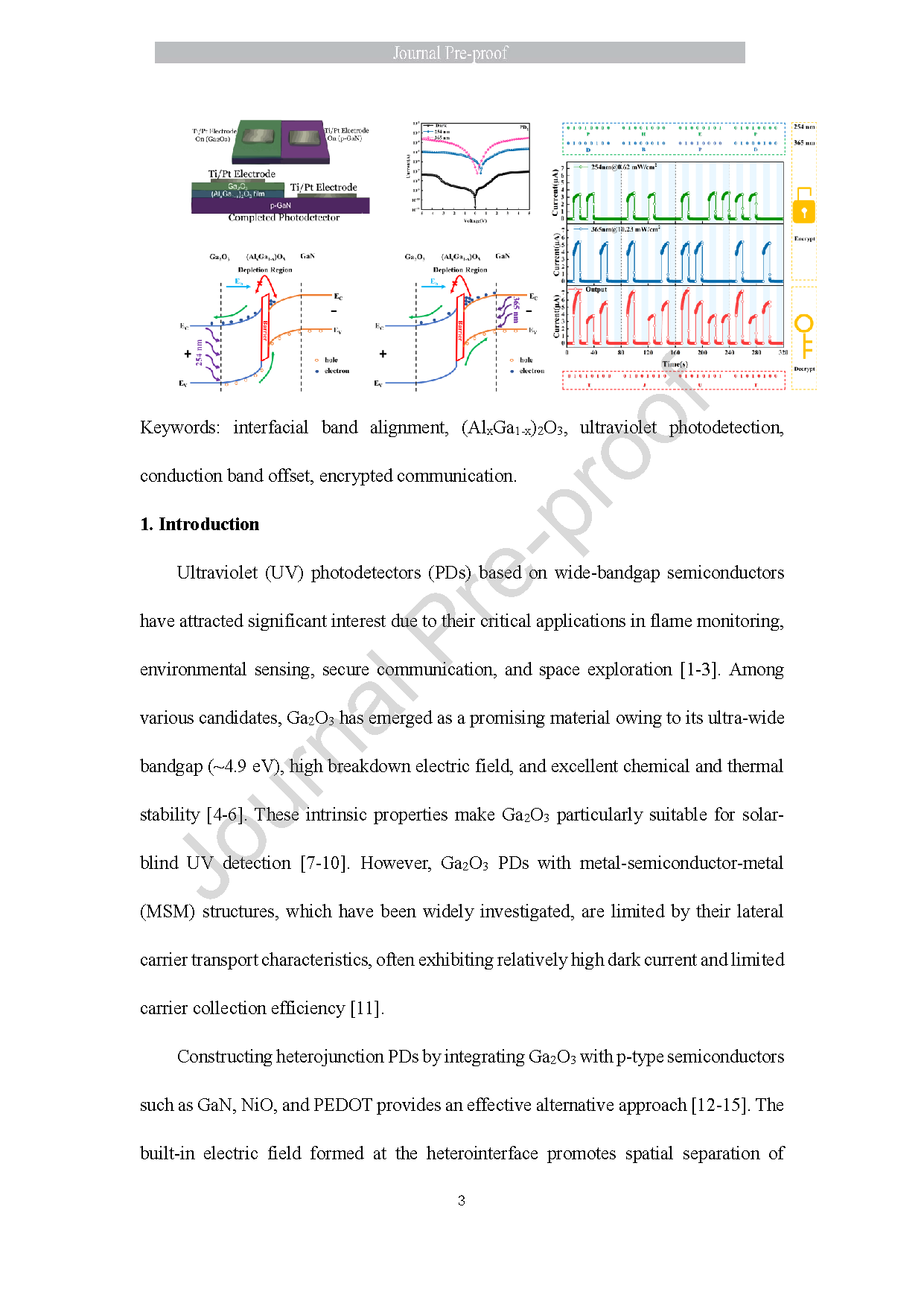
Interfacial band alignment plays a decisive role in determining carrier transport and recombination dynamics in ultra-wide-bandgap heterojunction photodetectors. Here, we report a composition-tunable Ga₂O₃/(AlₓGa₁₋ₓ)₂O₃/GaN heterostructure for ultraviolet photodetection, in which a thin (AlₓGa₁₋ₓ)₂O₃ interlayer is introduced to engineer asymmetric band discontinuities. X-ray photoelectron spectroscopy reveals that inserting (Al0.15Ga0.85)₂O₃ significantly enhances the conduction band offset (ΔEC ≈ 1.90 eV at the GaN interface) while only marginally modifying the valence band alignment, enabling electron-selective blocking and efficient hole transport. Systematic composition modulation demonstrates a non-monotonic dependence of device performance on Al content, governed by the competition between barrier-induced carrier separation and defect-assisted recombination in the amorphous interlayer. The optimized device exhibits markedly enhanced responsivity and detectivity under both 254 nm and 365 nm illumination, together with accelerated transient response. Benefiting from its intrinsic broadband photoresponse, the heterostructure further enables photonic logic operations for ultraviolet encrypted communication. This work provides a physically grounded strategy for carrier-selective band engineering in Ga₂O₃-based heterostructures toward high-performance multifunctional UV photodetectors.
Highlights
Interface band engineering via a tunable (AlₓGa₁₋ₓ)₂O₃interlayer.
Optimized Al content balances barrier enhancement and defect-induced recombination.
Enhanced band offset enables efficient carrier separation and low dark current.
Shows promise for secure UV communication via logic operations.
Conclusion
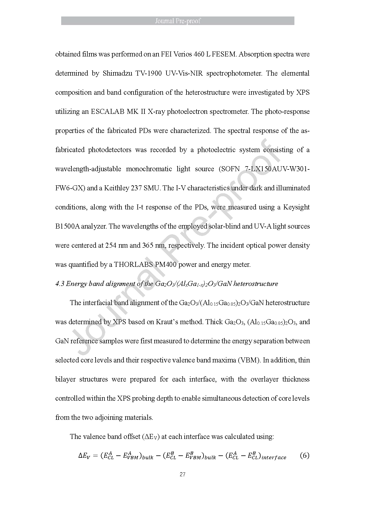
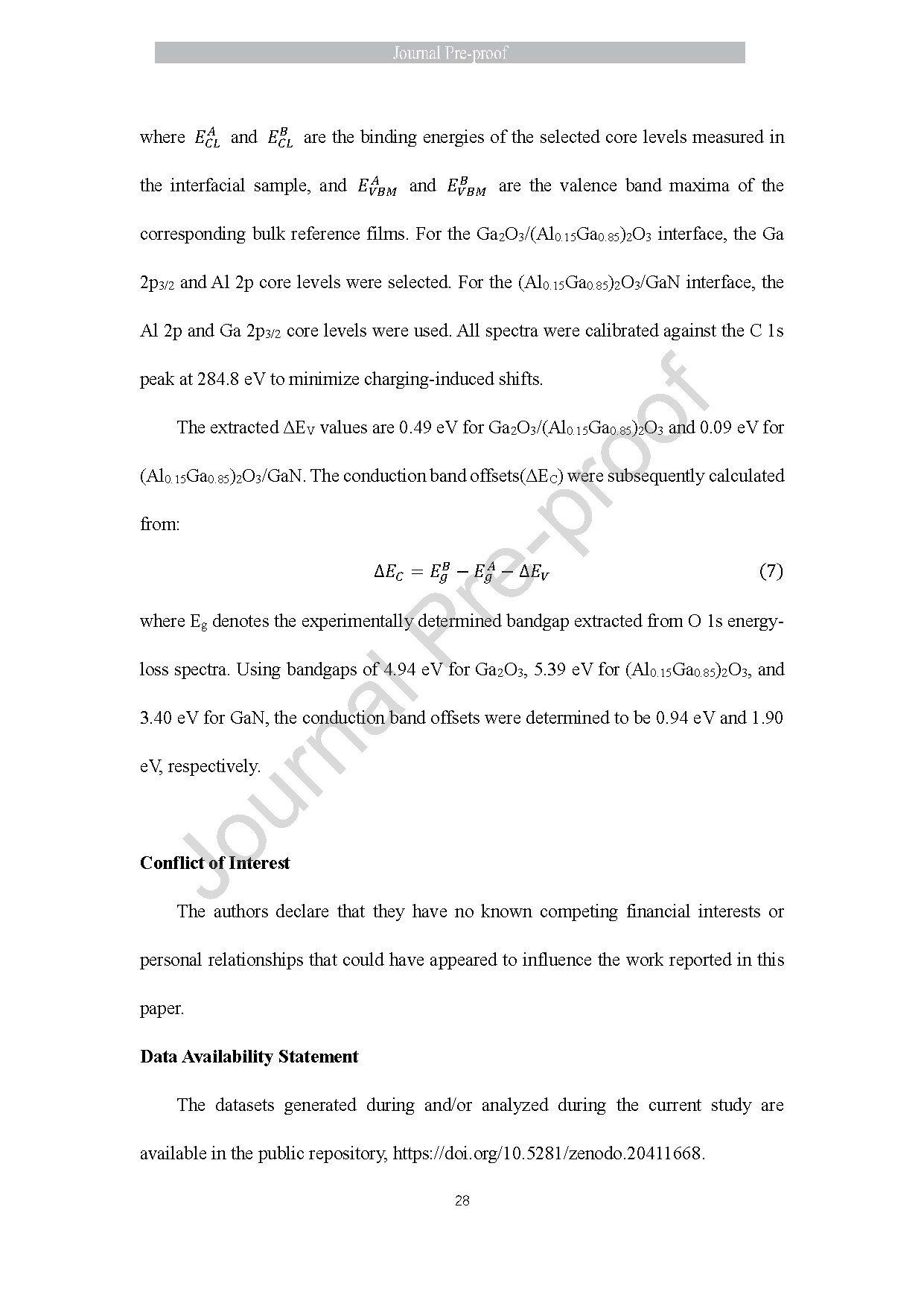
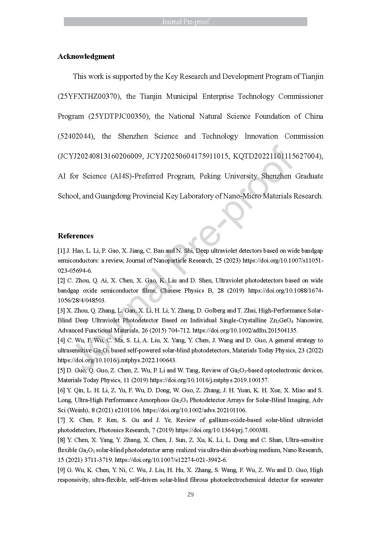
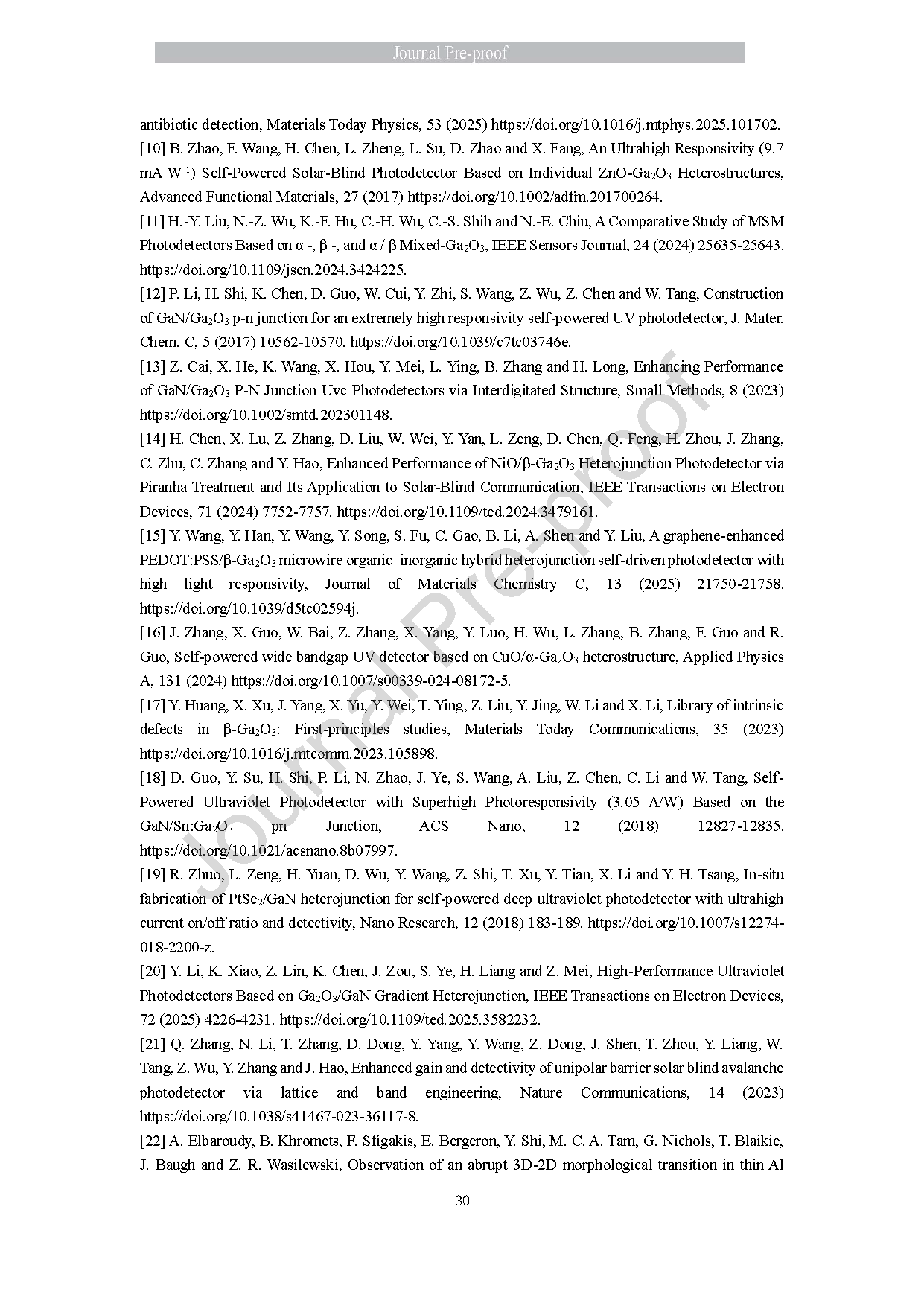
In summary, we have demonstrated a composition-engineered Ga₂O₃/(AlₓGa₁₋ₓ)₂O₃/GaN heterojunction in which interfacial band alignment is deliberately tailored to regulate carrier-selective transport. XPS-based band offset analysis reveals that the insertion of an optimized (Al0.15Ga0.85)₂O₃ interlayer substantially increases the conduction band discontinuity while maintaining a small valence band offset, establishing an asymmetric carrier-blocking configuration. Systematic comparison across different Al compositions uncovers a non-monotonic performance evolution arising from the competition between barrier-enhanced carrier separation and defect-mediated recombination in the amorphous interlayer. The optimized heterostructure achieves enhanced responsivity, detectivity and faster transient response under both solar-blind and UV-A illumination. Beyond performance improvement, this study clarifies the physical role of composition-tunable ultra-wide-bandgap interlayers in controlling band discontinuities and carrier dynamics. The demonstrated strategy provides a generalizable platform for band-selective engineering in oxide/III-V heterostructures and offers new opportunities for multifunctional ultraviolet optoelectronic systems.
Project Support
This work is supported by the Key Research and Development Program of Tianjin (25YFXTHZ00370), the Tianjin Municipal Enterprise Technology Commissioner Program (25YDTPJC00350), the National Natural Science Foundation of China (52402044), the Shenzhen Science and Technology Innovation Commission (JCYJ20240813160206009, JCYJ20250604175911015, KQTD20221101115627004), AI for Science (AI4S)-Preferred Program, Peking University Shenzhen Graduate School, and Guangdong Provincial Key Laboratory of Nano-Micro Materials Research.
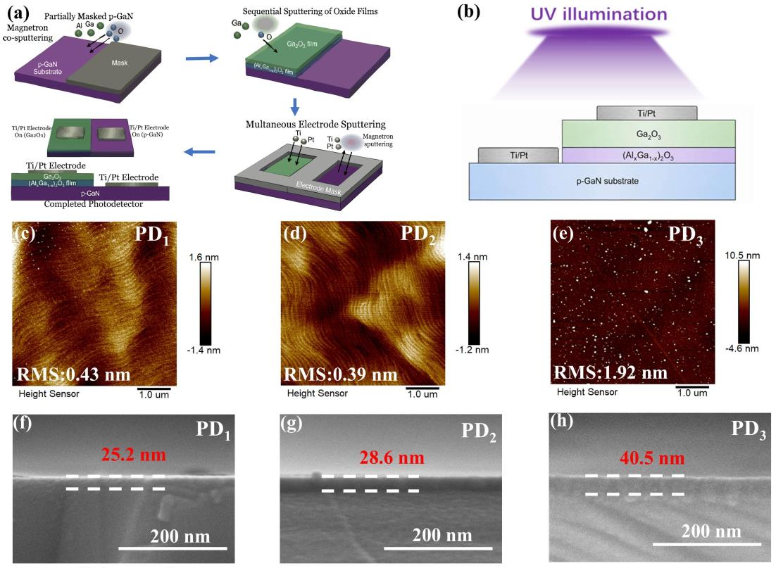
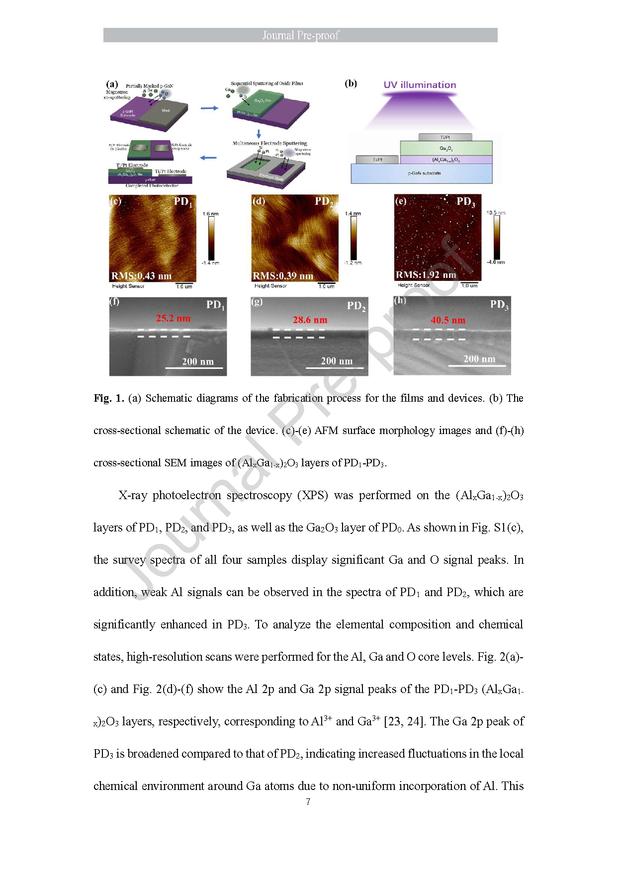
Fig. 1. (a) Schematic diagrams of the fabrication process for the films and devices. (b) The cross-sectional schematic of the device. (c)-(e) AFM surface morphology images and (f)-(h) cross-sectional SEM images of (AlₓGa₁₋ₓ)₂O₃ layers of PD₁-PD₃.
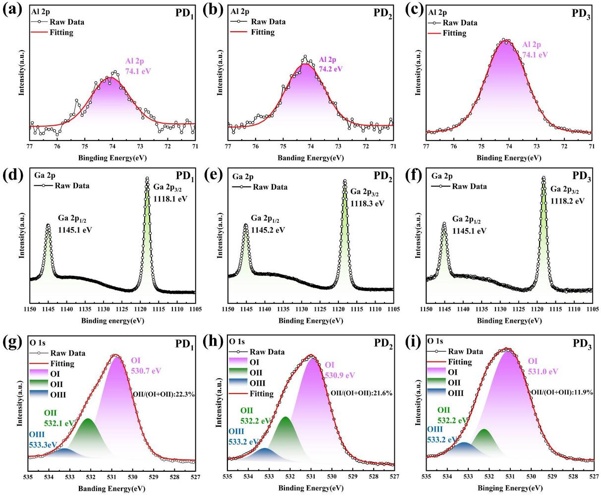
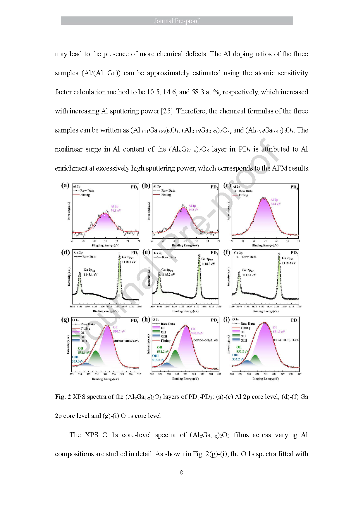
Fig. 2 XPS spectra of the (AlₓGa₁₋ₓ)₂O₃ layers of PD₁-PD₃: (a)-(c) Al 2p core level, (d)-(f) Ga 2p core level and (g)-(i) O 1s core level.
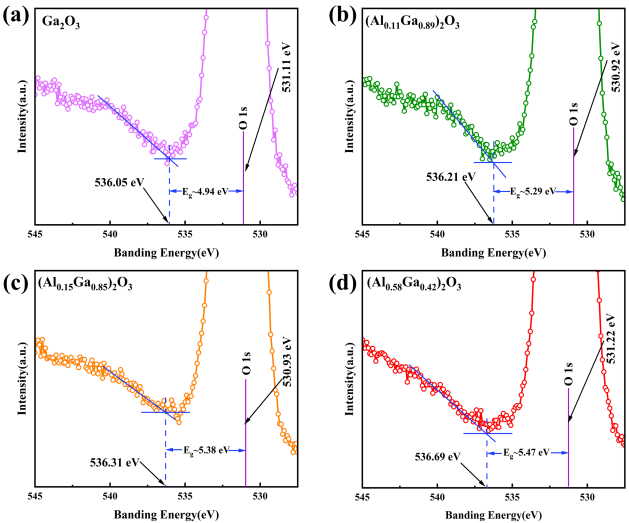
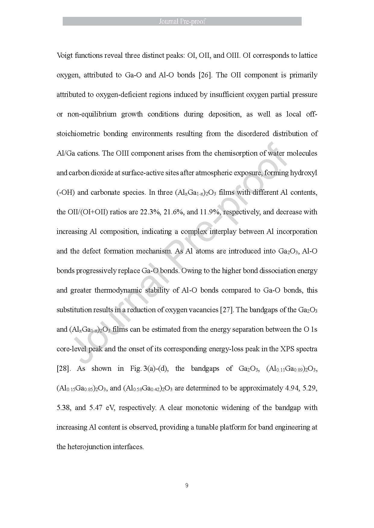
Fig. 3. Bandgap energies of (a) Ga₂O₃ film and (b)-(d) (AlₓGa₁₋ₓ)₂O₃ films with different Al contents, determined from the energy separation between the center of the O 1s core-level and the onset of its corresponding energy-loss feature.
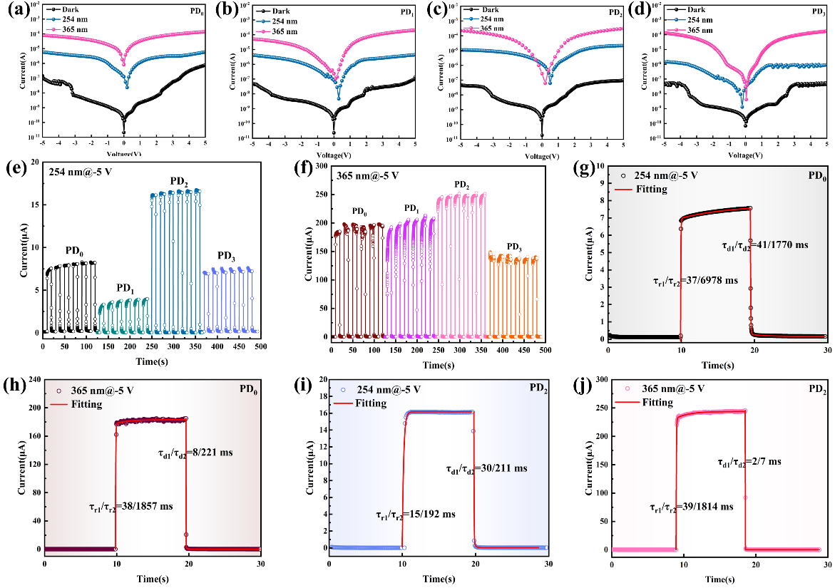
Fig. 4. (a)-(d) Semi-logarithmic I-V characteristics of PD₀-PD₃ under dark conditions and 254 and 365 nm UV illumination. I-t curves of PD₀-PD₃ under (e) 254 nm and (f) 365 nm illumination at a bias of -5 V. Expanded views of the single-cycle rise and decay edges with the corresponding exponential fits for (g)(h) PD₀ and (i)(j) PD₂.
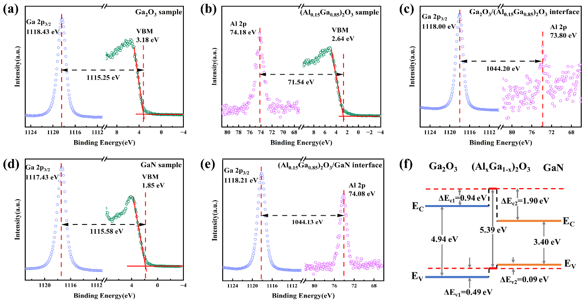
Fig. 5. (a) The Ga 2p3/2 core level spectrum and the valence band spectrum of Ga₂O₃ sample. (b) The Al 2p core level spectrum and the valence band spectrum of (Al0.15Ga0.85)₂O₃ sample. (c) XPS spectra of the Ga 2p3/2 and Al 2p core levels at the Ga₂O₃/(Al0.15Ga0.85)₂O₃ interface; (d) The Ga 2p3/2 core level spectrum and the valence band spectrum of GaN sample. (e) XPS spectra of the Ga 2p3/2 and Al 2p core levels at the (Al0.15Ga0.85)₂O₃/GaN interface. (f) Band structure schematic of the Ga₂O₃/(AlₓGa₁₋ₓ)₂O₃/GaN heterojunction.
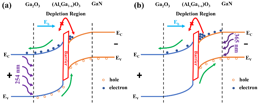
Fig. 6. Energy band diagrams of the heterojunction under various conditions: (a) reverse bias with 254 nm light illumination, and (b) reverse bias with 365 nm light illumination.
DOI:
doi.org/10.1016/j.jallcom.2026.190296
Instruction
Official Account

Cooperation
Top
