


Researchers from Xiamen University, Shenzhen Research Institute of Xiamen University have published a paper titled "2.7-kV CuCrO₂/Ga₂O₃ heterojunction diode with stepped-mesa termination and on-state electrical stress reliability" in Applied Physics Letters.
Background
β-Ga₂O₃ with an ultra-wide bandgap of 4.9 eV and ultrahigh theoretical breakdown field acts as core material for high-voltage power rectifiers, while its intrinsic n-type conductivity restricts the fabrication of bipolar devices. P-type oxide heterojunctions are the mainstream technical route. CuCrO₂ possesses favorable p-type conductivity, wide optical bandgap and high-temperature chemical stability, matching the process window of Ga₂O₃ power devices. Conventional planar field plate terminals suffer severe electric field crowding at device edges, resulting in low breakdown voltage and failing kV-level power equipment requirements. Existing researches only compare static blocking and conduction performance, without systematic evaluation of long-term on-state electrical stress reliability; the trap transport mechanism corresponding to device degradation also lacks quantitative analysis. Current Ga₂O₃ heterojunction diodes lack stepped termination architectures that simultaneously realize high breakdown voltage, low specific on-resistance and anti-stress stability, and cannot satisfy both static performance and long-term operational reliability, forming a critical technical gap for the industrialization of ultra-wide bandgap power devices.
Abstract
In this work, we report vertical CuCrO₂/β-Ga₂O₃ p-n heterojunction diodes (HJDs) incorporating a stepped-mesa termination for enhanced blocking performance and robust on-state reliability. The optimized HJD achieves a breakdown voltage of 2.71 kV with a specific on-resistance of 5.84 mΩ・cm², corresponding to a power figure of merit of 1.3 GW/cm². TCAD simulations reveal that the stepped-mesa structure effectively suppresses electric-field crowding at the termination edge, accounting for the improved blocking capability. The onstate stability is further evaluated using a measurement-stress-measurement protocol under both constant-voltage and constant-current stress conditions. The HJD exhibits an essentially unchanged turn-on voltage and a minor increase in dynamic on-resistance, with the stress-induced variation being largely reversible after stress removal. Temperature-dependent reverse-current analysis suggests that the high-field leakage is governed by trap-assisted Poole–Frenkel emission, yielding a trap barrier height of ~0.35 eV. By correlating the recoverable stress response with the leakage-mechanism analysis, the stressinduced electrical variation is mainly associated with reversible electron capture and emission in pre-existing trap states. This work demonstrates that stepped-mesa-terminated CuCrO₂/β-Ga₂O₃ HJDs provide a promising route toward reliable kilovolt-class ultra-wide-bandgap power rectifiers.
Highlights
Propose a stepped-mesa edge termination structure for vertical CuCrO₂/β-Ga₂O₃heterojunction diodes to alleviate peripheral electric field crowding.
Realize 2.71 kV breakdown voltage and 5.84 mΩ·cm² specific on-resistance, with a power figure of merit up to 1.3 GW/cm².
Systematically evaluate device reliability under constant voltage and constant current on-state stress, with recoverable electrical drift after stress release.
Clarify reverse leakage follows Poole–Frenkel emission with 0.35 eV trap barrier, attribute stress variation to reversible trap electron capture and emission.
Conclusion
In summary, we demonstrated high-performance vertical CuCrO₂/β-Ga₂O₃ HJDs incorporating an optimized stepped-mesa termination, achieving a high Vbr of 2.71 kV while maintaining a low Ron,sp of 5.84 mΩ・cm². Under prolonged on-state electrical stress, the device exhibited excellent parametric stability, with an essentially unchanged Von and only limited increases in dynamic Ron,sp of 6.3% and 6.7% after 1000 s under CVS and CCS, respectively. Temperature-dependent reverse-current analysis further indicated that the high-field leakage was mainly associated with trap-assisted Poole–Frenkel emission, yielding a trap barrier height of approximately 0.35 eV. By correlating the leakage mechanism with the on-state stress behavior, the stress-induced electrical variation was primarily attributed to reversible electron capture and emission involving pre-existing trap states. These results suggest that stepped-mesa-terminated CuCrO₂/β-Ga₂O₃ HJDs can combine kilovolt-class blocking capability with robust on-state electrical-stress reliability, providing potential device-design approach for Ga₂O₃-based bipolar power rectifiers.
Project Support
This work was supported by the Shenzhen Science and Technology Program under Grant JCYJ20240813145617023, and the National Natural Science Foundation of China under Grant 62171396.
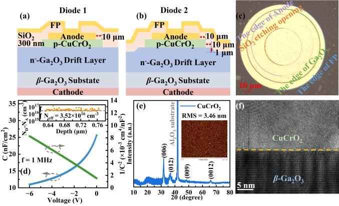
FIG. 1. Cross-sectional schematics of (a) reference Diode 1 and (b) Diode 2 with a stepped-mesa termination. (c) Top-view optical micrograph of the fabricated Diode 2. (d) C–V and 1/C²–V characteristics of Diode 2 measured at 1 MHz. The inset shows the extracted net carrier concentration profile of the β-Ga₂O₃ drift layer. (e) XRD pattern of the sputtered CuCrO₂ film deposited on an Al₂O₃ substrate. The inset shows the corresponding AFM surface morphology. (f) Cross-sectional HRTEM image of the CuCrO₂/β-Ga₂O₃ heterointerface.
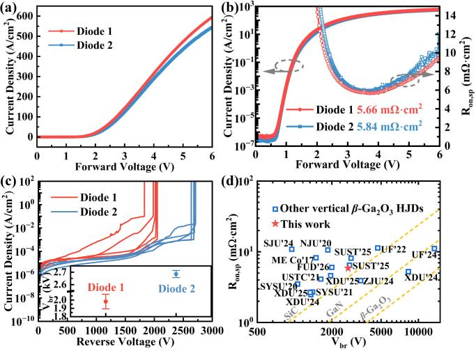
FIG. 2. (a) Linear-scale forward J–V characteristics of Diode 1 and Diode 2. (b) Semi-logarithmic forward J–V curves and extracted Ron,sp as a function of bias. (c) Semi-logarithmic reverse breakdown characteristics of five independently measured devices with Diode 1 and Diode 2 structures. The inset summarizes the Vbr statistics, where symbols and error bars represent the mean values and standard deviations, respectively. (d) Benchmark comparison of Ron,sp versus Vbr with state-of-the-art small-area vertical β-Ga₂O₃ HJDs.
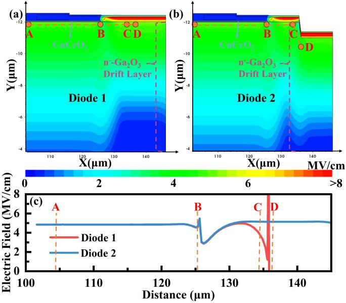
FIG. 3. Two-dimensional electric field contours at a reverse bias of 2 kV for (a) Diode 1 and (b) Diode 2. (c) Extracted one-dimensional electric field profiles of Diode 1 and Diode 2 along the A–B–C–D cutline.
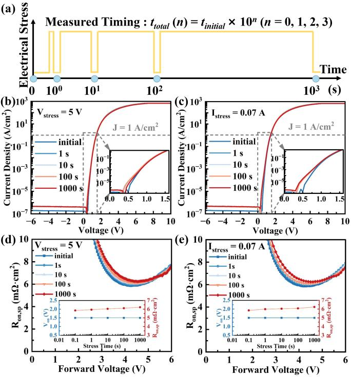
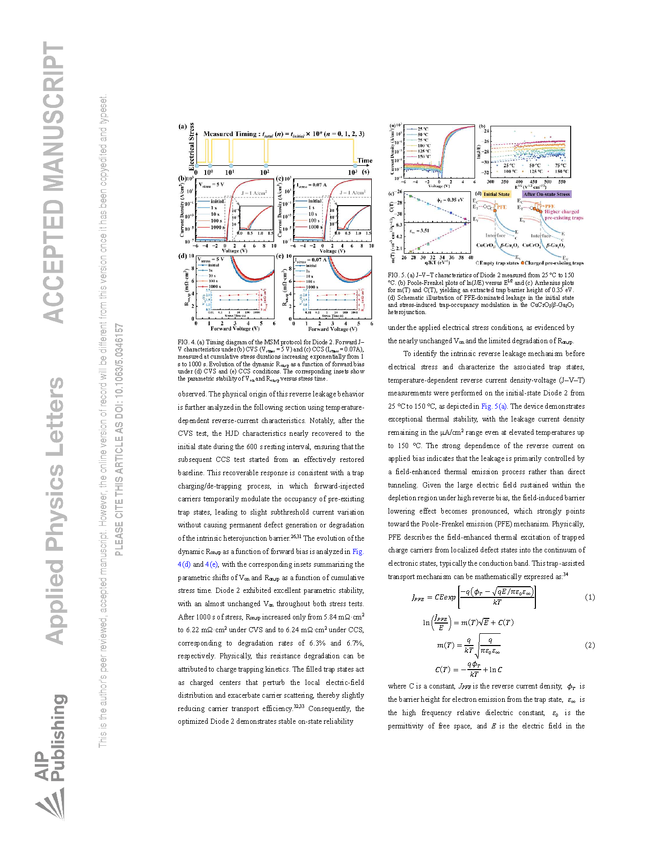
FIG. 4. (a) Timing diagram of the MSM protocol for Diode 2. Forward J–V characteristics under (b) CVS (Vstress = 5 V) and (c) CCS (Istress = 0.07 A), measured at cumulative stress durations increasing exponentially from 1 s to 1000 s. Evolution of the dynamic Ron,sp as a function of forward bias under (d) CVS and (e) CCS conditions. The corresponding insets show the parametric stability of Von and Ron,sp versus stress time.
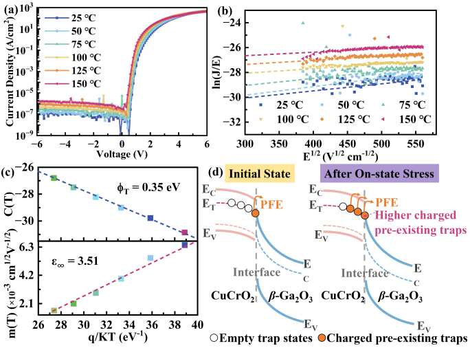
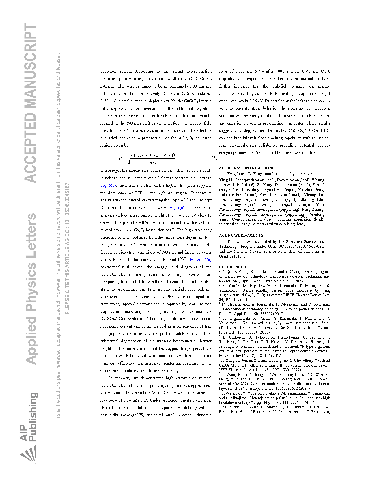
FIG. 5. (a) J–V–T characteristics of Diode 2 measured from 25 °C to 150 °C. (b) Poole-Frenkel plots of ln (J/E) versus E¹ᐟ² and (c) Arrhenius plots for m (T) and C (T), yielding an extracted trap barrier height of 0.35 eV. (d) Schematic illustration of PFE-dominated leakage in the initial state and stress-induced trap-occupancy modulation in the CuCrO₂/β-Ga₂O₃ heterojunction.
DOI:
https://doi.org/10.1063/5.0346157
Instruction
Official Account

Cooperation
Top
