


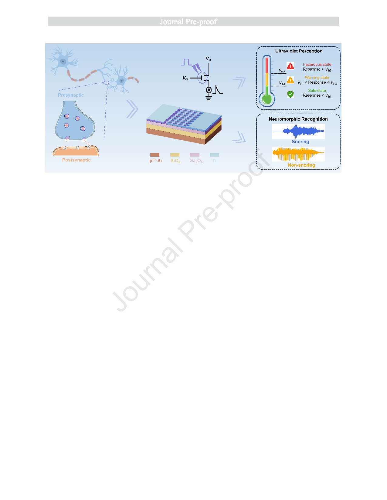
Researchers from the College of Medical Information and Artificial Intelligence, Shandong First Medical University & Shandong Academy of Medical Sciences; the School of Information Science and Engineering, Qilu Normal University; the School of Integrated Circuits, Shandong University; the Institute of Nanoscience and Applications, College of Engineering, Southern University of Science and Technology; and the School of Electrical and Electronic Engineering, University of Manchester have published a dissertation titled "Room-temperature processable amorphous Ga₂O₃ synaptic transistor for solar-blind ultraviolet perception" in Journal of Materiomics.
Background
Neuromorphic computing has emerged to address the energy inefficiency of traditional architectures. Artificial synaptic devices, as core building blocks, emulate learning, memory, and information processing. Purely electrical operation suffers from crosstalk and high power consumption, whereas optoelectronic synapses offer a new pathway for low-energy computing by directly responding to optical signals.
Ga₂O₃ features a bandgap of ~4.9 eV, enabling highly selective solar-blind UV photoresponse, along with high breakdown field, excellent thermal stability, and radiation tolerance. Crystalline Ga₂O₃ devices deliver outstanding performance, but high-temperature crystallization limits their compatibility with flexible and wearable applications.
Amorphous Ga₂O₃ (a-Ga₂O₃) can be deposited at room temperature via sputtering, offering low cost and broad substrate compatibility. Its oxygen-vacancy-related persistent photoconductivity, while detrimental to fast response, is intrinsically beneficial for optoelectronic synapses, supporting prolonged postsynaptic current retention and temporal accumulation of optical stimuli. Moreover, the ultra-wide bandgap inherently suppresses long-wavelength interference, ensuring solar-blind specificity.
Most reported Ga₂O₃ synaptic devices are limited to two-terminal structures, whereas three-terminal transistors offer greater flexibility via gate-tunable carrier modulation. However, a device that simultaneously combines solar-blind UV selectivity, room-temperature processability, low-energy synaptic plasticity, and gate-programmable operation has not yet been demonstrated.
Abstract
Gallium oxide (Ga₂O₃)-based optoelectronic synapses are promising for solar-blind neuromorphic perception, yet their practical applications is currently hindered by energy consumption issues and the high fabrication temperature commonly required for crystalline devices. Herein, a room-temperature processable amorphous Ga₂O₃ synaptic transistor is developed to simultaneously achieve deep-ultraviolet photodetection and optoelectronic synaptic plasticity. Under 254 nm illumination, the device exhibits a photo-to-dark current ratio of 3.32×10⁷, a responsivity of 8.9×10³ A·W⁻¹, and a detectivity of 1.96×10¹⁷ Jones. These key parameters are comparable to those of crystalline Ga₂O₃ photodetectors. The transistor further emulates essential synaptic behaviors, including short-term memory, long-term memory, paired-pulse facilitation, and learning-forgetting-relearning behaviors, together with an ultralow energy consumption of 127.42 fJ per pulse. Benefiting from the intrinsic solar-blind response and defect-assisted persistent photoconductivity of a-Ga₂O₃, the device enables graded UV warning perception and sensitization response emulation. In addition, the experimentally obtained synaptic dynamics are used to demonstrate the potential of the device for temporal information processing in a reservoir-computing framework. This work establishes room-temperature amorphous Ga₂O₃ as a promising platform for low-energy solar-blind optoelectronic synapses and bio-inspired ultraviolet perception.
Highlights
①Room-temperature processable solar-blind UV perception synaptic transistor: A room-temperature processable amorphous Ga₂O₃ synaptic transistor enables solar-blind ultraviolet perception without high-temperature crystallization processes.
②Outstanding photodetection performance: Responsivity of 8.9×10³ A·W⁻¹ and photo-to-dark current ratio of 3.32×10⁷ are achieved, with key parameters comparable to crystalline Ga₂O₃ devices.
③Defect-assisted low-energy synaptic plasticity: Defect-assisted synaptic plasticity is realized with ultralow energy consumption of 127.42 fJ per pulse.
④Graded UV warning and reservoir computing based snoring recognition: Graded UV warning and reservoir computing based snoring recognition are demonstrated.
Conclusion
In summary, a room-temperature processable a-Ga₂O₃ synaptic transistor is demonstrated that combines high-performance solar-blind UV photodetection with low-energy optoelectronic synaptic plasticity. The optimized device exhibits a PDCR of 3.32×10⁷, an EQE of 4.36×10⁶ %, a R of 8.9×10³ A·W⁻¹, and a D* of 1.96×10¹⁷ Jones. Owing to the defect-assisted persistent photoconductivity of the a-Ga₂O₃ channel, the transistor operates at an ultralow energy consumption of only 127.42 fJ per spike, while successfully emulating key synaptic functions, such as STM, LTM, PPF, and learning-forgetting-relearning behavior. Furthermore, the device enables a proof of concept UV warning perception model and shows potential for temporal information processing when integrated with a RC scheme. Overall, the proposed a-Ga₂O₃ combines room-temperature processability, outstanding optoelectronic characteristics, and energy-efficient neuromorphic functionality. This highlights defect engineering as an effective route to simultaneously enhance synaptic energy efficiency and enable scalable oxide neuromorphic devices for next-generation flexible and wearable intelligent sensing systems.
Project Support
This work was supported in part by the Natural Science Foundation of Shandong Province under Grant ZR2024QE477 and Grant ZR2022ZD05, and in part by the National Key Research and Development Program of China under Grant 2022YFB3603900 and Grant 2022YFA1405200.
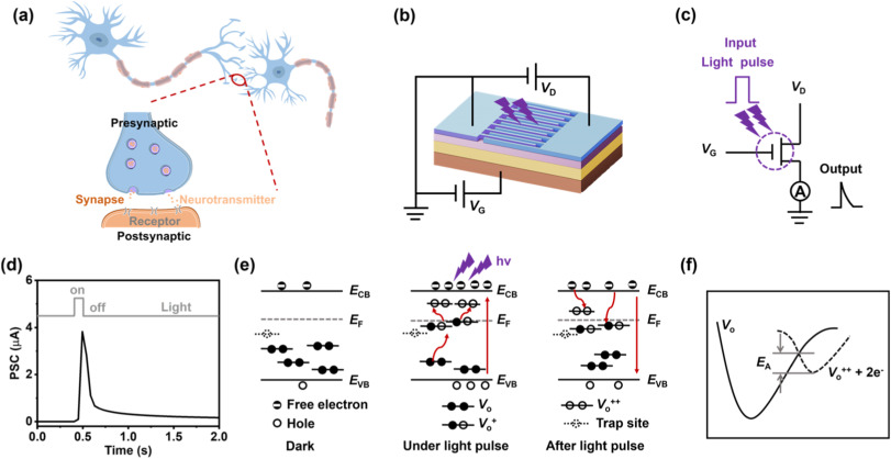
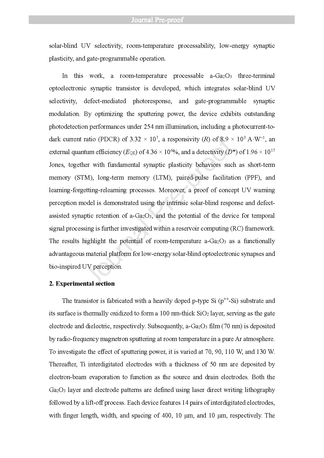
Fig. 1. Synaptic characteristics and operating mechanism of the a-Ga₂O₃ synaptic transistor. (a) Schematic diagram of the biological neuron and synapse. (b) Schematic circuit connection of the a-Ga₂O₃ transistor. (c) Circuit diagram of the a-Ga₂O₃ synaptic transistor. (d) PSC responses of Ga₂O₃ synaptic transistor with light intensity of 220.2 μW·cm⁻². (e) The energy band structure of the Ga₂O₃ film in dark, under light pulse, and after light pulse. (f) Schematic diagram of the activation energies (EA) for neutralization of ionized oxygen vacancies (Vₒ) for Ga₂O₃ synaptic transistor.
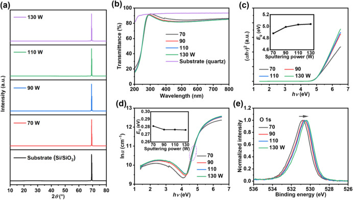
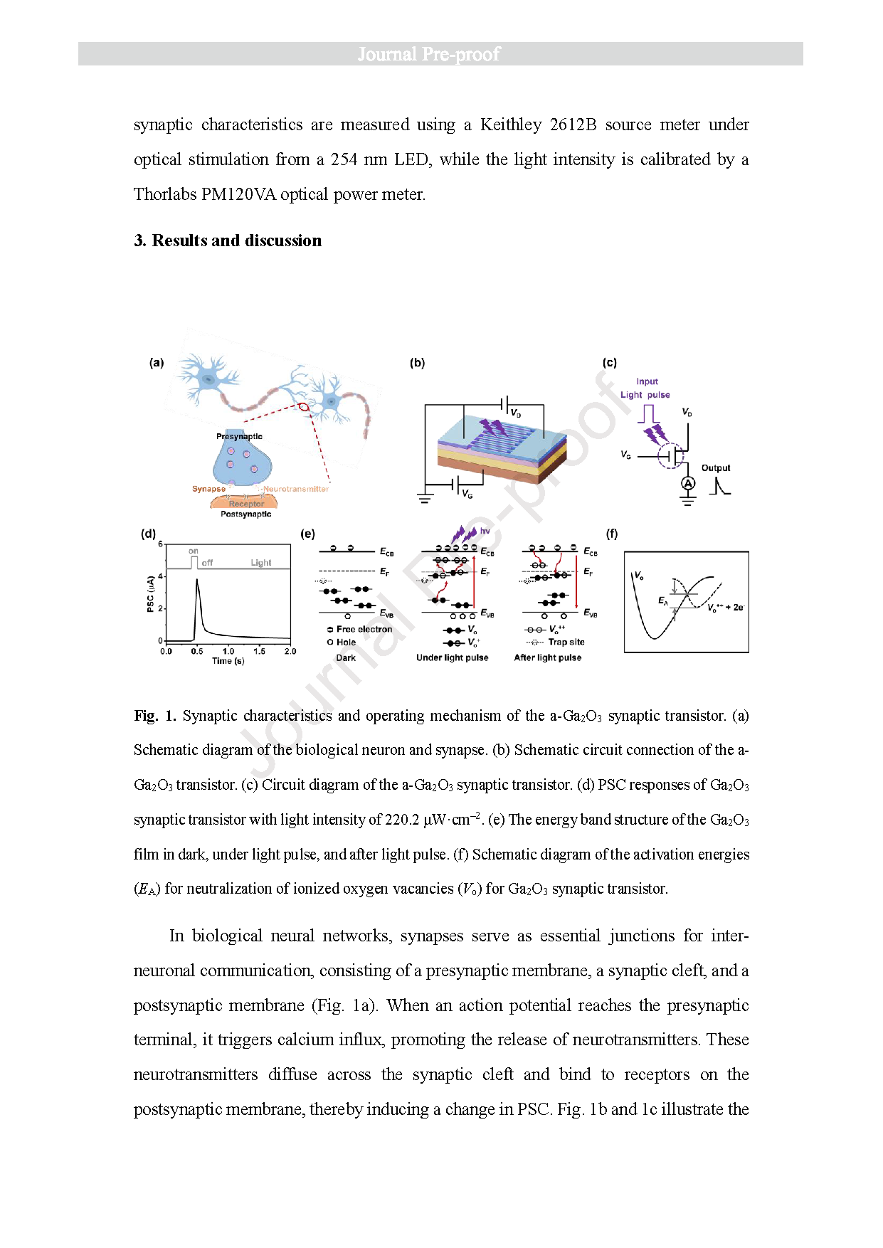
Fig. 2. Influence of different sputtering powers on the structure, optical property, and chemical state of Ga₂O₃ films. (a) XRD patterns of Ga₂O₃ films deposited at different sputtering powers. (b) Optical transmittance spectra of the Ga₂O₃ films deposited at different sputtering powers. (c) (αhv)²-hv plots, with the inset showing optical bandgap as a function of sputtering power. (d) lnα–hv plots, with the inset showing the Urbach energy as a function of sputtering power. (e) O 1s XPS spectra of Ga₂O₃ films deposited at different sputtering powers.
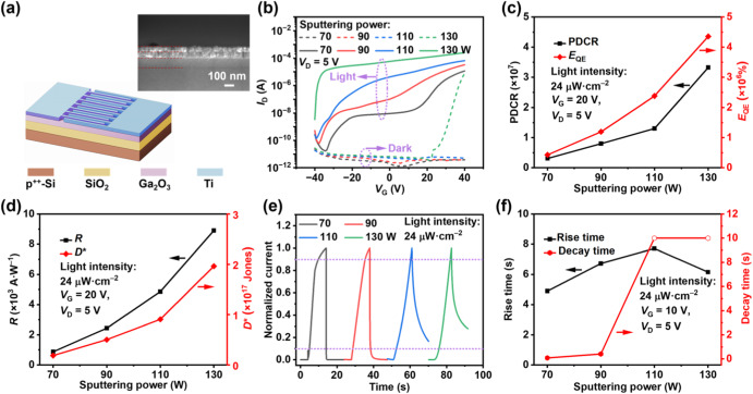
Fig. 3. Influence of different sputtering powers on the photoelectric detection performance of a-Ga₂O₃ devices. (a) Schematic diagram of the a-Ga₂O₃ device structure. The inset image shows the cross-sectional SEM of the a-Ga₂O₃ device. (b) Transfer characteristics of the a-Ga₂O₃ devices measured under dark and light. (c) Variation of the PDCR and EQE with sputtering power. (d) Variation of the R and D* with sputtering power. (e) Normalized time-dependent response curves. (f) Variation of rise time and decay time as a function of sputtering power.
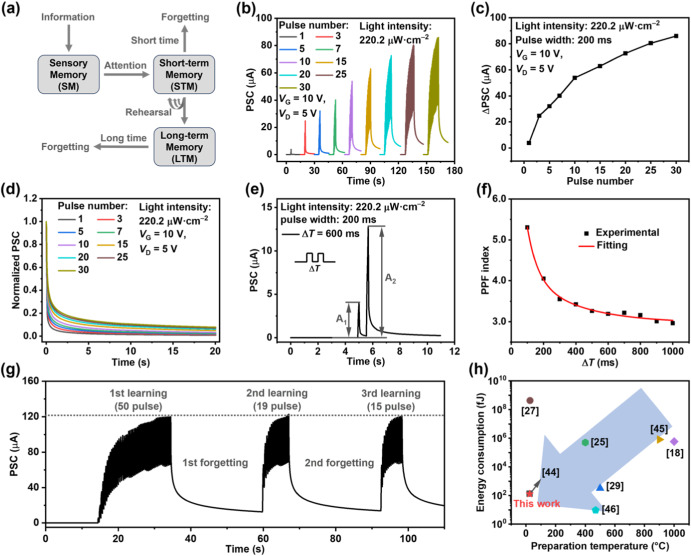
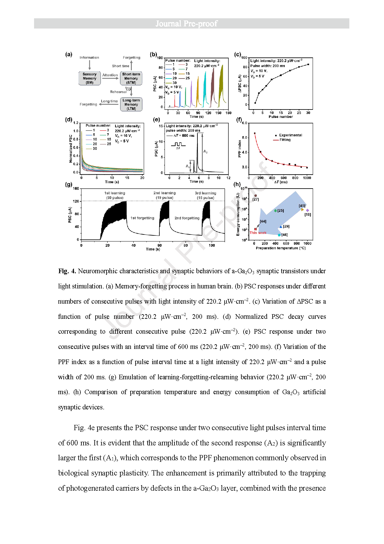
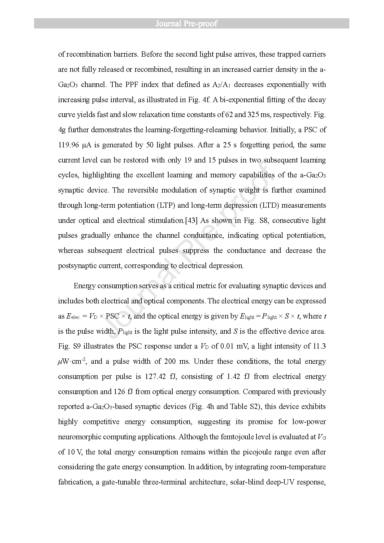
Fig. 4. Neuromorphic characteristics and synaptic behaviors of a-Ga₂O₃ synaptic transistors under light stimulation. (a) Memory-forgetting process in human brain. (b) PSC responses under different numbers of consecutive pulses with light intensity of 220.2 μW·cm⁻². (c) Variation of ΔPSC as a function of pulse number (220.2 μW·cm⁻², 200 ms). (d) Normalized PSC decay curves corresponding to different consecutive pulse (220.2 μW·cm⁻²). (e) PSC response under two consecutive pulses with an interval time of 600 ms (220.2 μW·cm⁻², 200 ms). (f) Variation of the PPF index as a function of pulse interval time at a light intensity of 220.2 μW·cm⁻² and a pulse width of 200 ms. (g) Emulation of learning-forgetting-relearning behavior (220.2 μW·cm⁻², 200 ms). (h) Comparison of preparation temperature and energy consumption of Ga₂O₃ artificial synaptic devices.
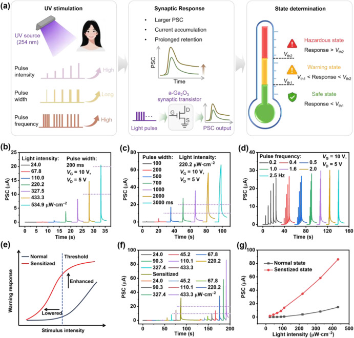
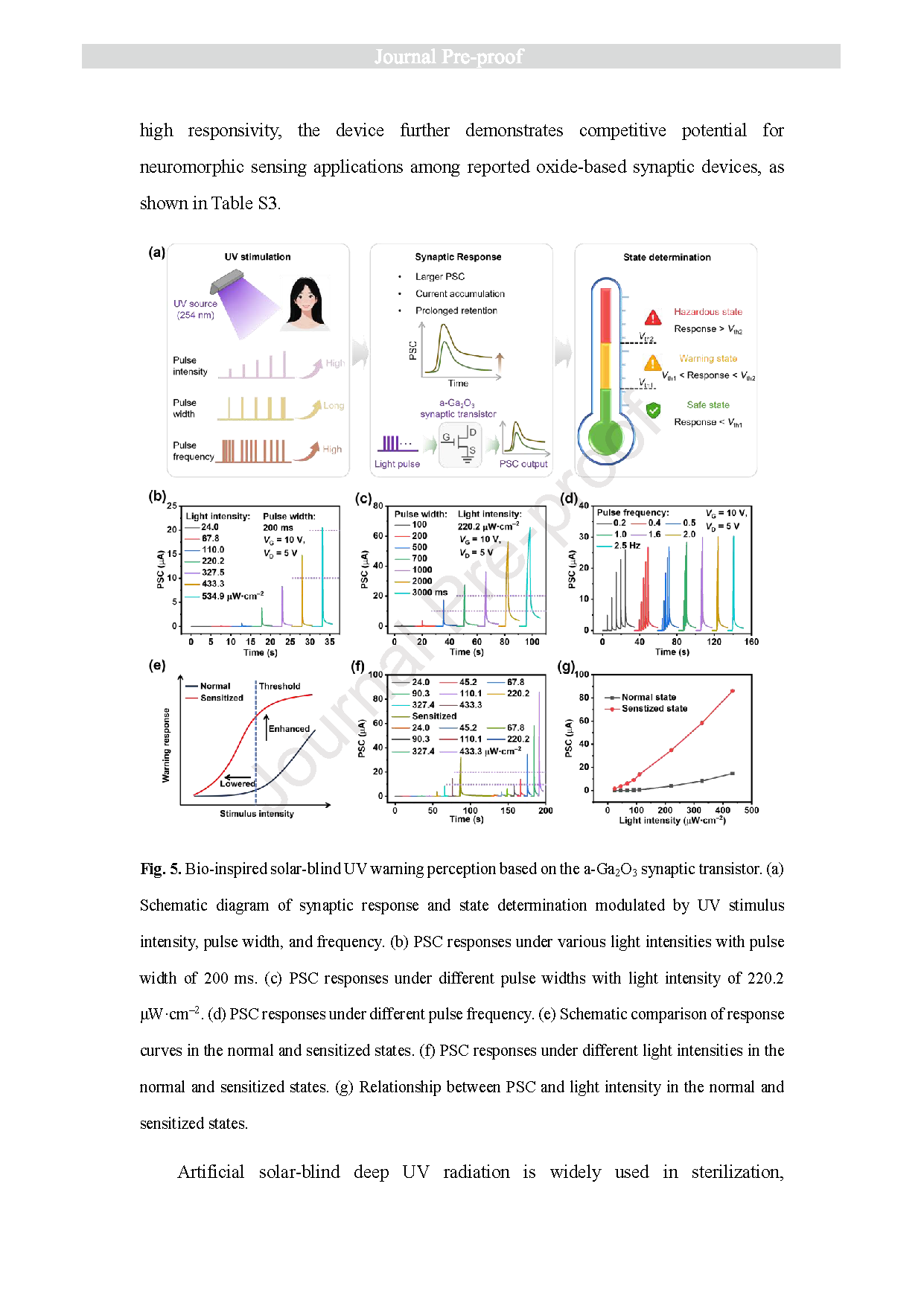
Fig. 5. Bio-inspired solar-blind UV warning perception based on the a-Ga₂O₃ synaptic transistor. (a) Schematic diagram of synaptic response and state determination modulated by UV stimulus intensity, pulse width, and frequency. (b) PSC responses under various light intensities with pulse width of 200 ms. (c) PSC responses under different pulse widths with light intensity of 220.2 μW·cm⁻². (d) PSC responses under different pulse frequency. (e) Schematic comparison of response curves in the normal and sensitized states. (f) PSC responses under different light intensities in the normal and sensitized states. (g) Relationship between PSC and light intensity in the normal and sensitized states.
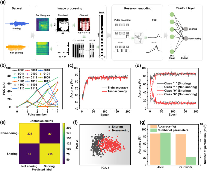
Fig. 6. Snoring recognition capability of a-Ga₂O₃ synaptic transistors. (a) Schematic diagram of the snore recognition. (b) PSC responses under 4-bit, 16-pulse sequences. (c) Accuracy profiles for distinguishing snoring and non-snoring signals. (d) Classification curves for snoring and non-snoring signals in the "1" and "0" category folder of the dataset. (e) Confusion matrix of classification results. (f) Visualization of feature distribution using PCA. (g) Comparison of classification accuracy and the number of parameters between the RC framework and the single-layer linear ANN baseline.
DOI:
doi.org/10.1016/j.jmat.2026.101311

Instruction
Official Account

Cooperation
Top
